EP0131699B1 - Method and apparatus for controlling alignment and brightness of an electron beam - Google Patents
Method and apparatus for controlling alignment and brightness of an electron beam Download PDFInfo
- Publication number
- EP0131699B1 EP0131699B1 EP84104924A EP84104924A EP0131699B1 EP 0131699 B1 EP0131699 B1 EP 0131699B1 EP 84104924 A EP84104924 A EP 84104924A EP 84104924 A EP84104924 A EP 84104924A EP 0131699 B1 EP0131699 B1 EP 0131699B1
- Authority
- EP
- European Patent Office
- Prior art keywords
- aperture
- path
- center
- difference
- plate
- Prior art date
- Legal status (The legal status is an assumption and is not a legal conclusion. Google has not performed a legal analysis and makes no representation as to the accuracy of the status listed.)
- Expired
Links
- 238000010894 electron beam technology Methods 0.000 title claims description 26
- 238000000034 method Methods 0.000 title claims description 16
- 238000012937 correction Methods 0.000 description 29
- 238000012935 Averaging Methods 0.000 description 3
- 238000010586 diagram Methods 0.000 description 3
- 239000004065 semiconductor Substances 0.000 description 3
- 238000013459 approach Methods 0.000 description 2
- 230000000694 effects Effects 0.000 description 2
- 238000005259 measurement Methods 0.000 description 2
- 230000000737 periodic effect Effects 0.000 description 2
- 238000007493 shaping process Methods 0.000 description 2
- 230000001360 synchronised effect Effects 0.000 description 2
- 238000012360 testing method Methods 0.000 description 2
- 230000002457 bidirectional effect Effects 0.000 description 1
- 230000008878 coupling Effects 0.000 description 1
- 238000010168 coupling process Methods 0.000 description 1
- 238000005859 coupling reaction Methods 0.000 description 1
- 238000005070 sampling Methods 0.000 description 1
- 239000011800 void material Substances 0.000 description 1
Images

Classifications
-
- H—ELECTRICITY
- H01—ELECTRIC ELEMENTS
- H01J—ELECTRIC DISCHARGE TUBES OR DISCHARGE LAMPS
- H01J37/00—Discharge tubes with provision for introducing objects or material to be exposed to the discharge, e.g. for the purpose of examination or processing thereof
- H01J37/30—Electron-beam or ion-beam tubes for localised treatment of objects
- H01J37/304—Controlling tubes by information coming from the objects or from the beam, e.g. correction signals
Definitions
- This invention relates generally to a method and apparatus for controlling an electron beam and, more particularly, to a method and apparatus for correcting the alignment and brightness of an electron beam used for writing patterns on a target, such as a semiconductor wafer.
- U.S. Patent No. 3,644,700 and 3,900,736 disclose method and apparatus for controlling a square- shaped beam.
- the beam is deflected throughout a writing field on a semiconductor wafer to write a desired pattern on the wafer.
- the beam For the beam to be applied at the desired position on the wafer, the beam must be properly aligned.
- instability of the beam can be caused by mechnical, thermal or electrolastic influences, and this instability is manifested by lateral drifting of the electron beam.
- U.S. Patent No. 3,894,271 discloses a method and apparatus for correcting the beam alignment during blanking of the beam by sensing the amount of beam current passing through a special alignment aperture in a blanking plate located in the path of the beam; an up-date counter counts up and down for each increase and decrease, respectively, of sensed current during each alignment correction cycle, and the stored count is converted to an analog correction voltage which is applied to an alignment yoke to correct the beam alignment in the X- and Y-directions.
- U.S. Patent No. 4,000,440 discloses a similar method and apparatus for alternately correcting both the alignment and the brightness of the electron beam. IBM Technical Disclosure Bulletin, Vol. 19, No.
- pages 464-465 discloses a beam alignment system in which the alignment is carried out by double deflection of the beam before the beam enters a square aperture in a first plate; the beam is blanked by deflecting it from the central aperture in a second, following plate which acts as a current collector, thereby eliminating the need for a separate offset alignment aperture as disclosed in U.S. Patent No. 3,894,271.
- controlling an electron beam passing from an electron beam source through a first aperture in a first plate is characterised by the steps of cyclically scanning the beam across the aperture equal distances from, and in opposite direction along a first path through the initial position of the centre of the beam, wherein the scan amplitude is sufficiently large for the beam, when centred, to strike opposite edges ofthe aperture, detecting the differences in average beam currents flowing through the aperture during adjacent half cycles of a scan cycle, and aligning the beam centre with the centre of the aperture by deflecting the beam from the initial position a distance related to said difference.
- the brightness of the beam can be controlled simultaneously with the correction of the beam alignment.
- a special aperture in a blanking plate is not necessarily required.
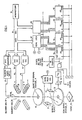
- electron gun 10 produces an electron beam 12 in the well-known manner.
- the beam is passed through a square spot-shaping aperture 14 in a plate 16 to form various square or rectangular shapes of the beam that have a minimum size equal to the minimum line width of the pattern that is to be written on a target 18, such as one of a plurality of chips on a semiconductor wafer mounted on a table 20 which is movable to different positions to place other chips in the target area.
- the beam then passes between a pair of blanking plates 21 and 22, and then through a beam-shaped aperture 24 in another plate 26.
- below plate 26 are deflection coils for efforting the actual writing of the beam on the target.
- Lenses, other electrolastic deflection plates, other apertures and other alignment sections may also be placed in the path of the electron beam for focusing and shaping the beam.
- the beam is blanked by applying a blank pulse across the blanking plate 21, 22 in order to deflect the beam from the central aperture 24 onto the plate 26 so that no writing occurs at this time on the wafer. It is during this blanking of the beam that the present invention dithers (cyclically scans) the beam across aperture 14 and corrects the alignment and current of the beam.
- the electron beam 12 also passes through an alignment yoke 28 located between the electron gun 10 and the plate 16.
- the yoke consists of a pair of X-direction deflection coils 30 and a pair of Y-direction deflection coils 32. It is to these deflection coils that the dithering signal and the respective X and Y direct current beam alignment currents are applied.
- the dithering and the alignment correction of the electron beam occurs while the beam is blanked, that is, while the beam is deflected by the blanking plates 21, 22 onto plate 26 and off the aperture 24.
- plate 26 collects the beam current which passes through the square aperture 14 in the plate 16 during a beam correction cycle.
- the collected currents are fed to circuits which form digital beam alignment and brightness control servos.
- Figure 2 illustrates the dithering signal and the control pulses required for the alignment and brightness correction cycle.
- a microprocessor 34 such as an Intel Corp. Model 8085, applies to a bidirectional data bus 36 a digital dithering signal which is synchronized with the available power line frequency, typically 50 or 60 Hz, i.e., the dither frequency is f/n, where f is the line frequency, and n is an integer.
- the microprocessor can easily accomplish said synchronization by sensing the zero crossings of the power line waveform and transmitting the digital dithering signal at the appropriate time to achieve synchronization thereof with the power line frequency.
- the digital dithering signal is transmitted simultaneously with a digital signal representing a D.C. voltage corresponding to any required correction of the beam alignment.
- the digital signals are applied via the data bus 36 to an X-direction digital-to-analog coverter (DAC) 38 which outputs via a line 40 to the X deflection coils 30 an analog current consisting of a periodic dither signal 42 superimposed upon a D.C. current corresponding to the required alignment correction current.
- DAC digital-to-analog coverter
- the dither signal and a corresponding Y-direction alignment correction digital signal are transmitted to a Y-direction digital-to-analog converter (DAC) 44 which applies a corresponding analog current via a line 46 to the Y-direction beam deflecting coils 32. Since the circuits for correcting the beam alignment in both the X and Y directions are the same, only the X corrections will be described in detail.
- the dithering signal 42 may be any periodic waveform in which adjacent half cycles are equal, it is preferred that the dithering signal 42 be an analog 50 Hz sinusoidal waveform synchronized with the power line frequency.
- the dithering signal could also be a digital approximation of such an analog signal.
- V/F voltage-to-fequency converter 50 operating in the 100 KHz range.
- Blanking of the beam is effected by applying a blank control pulse 4 to a blank pulse generator 52 which applies an appropriate blank pulse across the blanking plates 21, 22.
- the output of the V/F converter 50 is fed to one input of a NAND gate 54 which is enabled at its other input by a correction cycle control pulse 1.
- the frequency of the signal at the output of gate 54 is counted by a string of 4-bit up/ down counters 56, 58, 60 and 62 which are reset prior to the start of the dither by the reset control pulse 2.
- the number of counters depends on the measurement accuracy which is required.
- the up/down control signal 3 is up, whereby the counters count up during the positive half cycle of the dither signal 42.
- the counters store a count in which the most significant digit is a sign bit.
- the beam center is at the approximate center of the square aperture.
- the dither signal 42 then dithers the beam so that the beam is alternately scanned from the initial point in the X-direction back and forth at least far enough to intersect opposite edges of the aperture.
- the up/down control signal 3 is down so that the counters now count down from the positive count which had been stored in the preceding half cycle.
- the counters store a count and a sign indicating the magnitude and direction of the alignment correction which is required to centre the beam 12 on the square aperture 14. When the beam is aligned, the stored count is zero.
- a control pulse 5 transfers the count in the counters to corresponding octal latches 64, 66 etc., and then the control pulse 6 transfers the count from the latches to the data bus 36 and thus, to the microprocessor 34 which decides whether a correction is required and, if so, transmits to the DAC 38 a digital alignment correction signal as previously described. Correction of the beam alignment in the Y-direction is accomplished in the same manner by the use of the Y deflection coils 32, a digital alignment servo coupled to the output of the V/F converter 50, and the DAC 44.
- the counters 56, 58, 60, 62 etc. effectively average Area 1 and Area 2 under the respective half cycles of the dither signal 42 to determine the magnitude and direction of the beam alignment correction which is required in order to center the beam on the aperture 14.
- an immediate and almost total correction of the beam alignment is achieved, as compared to the slow, incremental correction produced by prior art methods and apparatus.
- the averaging is accomplished by counting several hundred pulses for each half cycle of the dither signal. More specifically, assuming a 60 Hz dither signal and a 100 KHz operating frequency of the V/F converter 50, the up/down counters will count over 800 pulses for each half cycle of the dither signal, after which the counts are algebraically summed (i.e.
- Area 2 is subtracted from Area 1) to produce the alignment correction current. Furthermore, in view of this large number of counts per half cycle, if there should be a void in the electron beam or if one pulse is obliterated by noise, the effect on the average of over 800 pulses is miniscule as compared to the prior art incremental alignment correction systems wherein a missed or erroneous pulse would have a very large effect on the alignment correction signal sent to the DAC. For example, 10 volts on the input of V/F converter 50 would be converted to a frequency of 100 KHz, and 5 volts to 50 KHz.
- this servo can move the beam to the center position. This case would represent a gross misalignment and would take more than one servo operation or correction cycle. If the beam totally misses the aperture, even including the dither, which might happen in a first alignment, the microprocessor could go into a raster mode where the beam alignment coils would move the beam in raster fashion until some beam current fell through the aperture.
- the alignment may also be corrected in both directions in the same cycle as illustrated in Fig. 3.
- the X dither signal 42 and a Y dither signal 68 are merely displaced in phase by 90° and applied simultaneously to the X and Y deflection coil pairs 30 and 32, respectively. If it is assumed that the magnitude of the dither signal is such that, when the beam is-centered in the aperture, the beam is dithered just to reach the opposite edge of the aperture, then the current passing through the aperture and collected by the plate 26 is constant as indicated by the dashed line 70 in Fig. 3.
- Fig. 4 illustrates, as an example, the manner in which the center of a circular beam moves relative to the center of a circular aperture when X and Y dither signals are applied simultaneously as illustrated in Fig. 3.
- the numbers in the counters after a few cycles of dither will be sufficient to tell the microprocessor how to move the D.C. alignment of the beam better to center it through the aperture.
- Such a circular approach is preferred if there is a significant amount of hysteresis in the magnetic deflection yoke 28.
- Such hysteresis would cause a delay between the dither and the actual beam positions, but this delay can be measured and compensated by appropriately delaying the changes of counting directions of the counters.
- the brightness of the electron beam can be controlled simultaneously with the correction of the beam alignment.
- a brightness servo has been disclosed in at least some of the above-cited prior art. Suffice it to say that a series of up counters 73 is connected to the output of the gate 54 so as to count in one direction the pulses from V/F converter 50 so that these counters, at the end of one dither cycle, store a count proportional to the total beam current collated by plate 26. In the manner just described with respect to the beam alignment correction, the count in the counter 73 is transferred via the data bus 36 and the microprocessor 34 to a brightness DAC 75 which outputs an analog D.C.
- the shape of the beam, the shape of the aperture, and the rotation of the beam with respect to the aperture are irrelevant to this invention.
- the synchronization of the dither signal with the local power line frequency is useful if there are some components of noise on the beam's position due to power line coupling.
- the power line deflection noise may change the amplitude of the dither, but the final result is not affected by such amplitude changes which are effectively cancelled out.
- the current measured is that of the beam which passed through the square aperture 14 and which was blanked onto the plate 26 containing the round aperture 24.
- the microprocessor 34 would then have to interpret the signs in the counters differently; the geometry considerations of the beam and apertures will determine which approach is preferable.
- the V/F converter 50 and the string of counters, such as 56, 58 etc. are convenient means of measuring the area under the aperture current curve by effectively taking thousands of samples in a few milliseconds; however, other methods of sampling and averaging the data could be used.
- the V/F converter and counters effectively take thousands of data samples, average them together, and subtract those taken during negative dither from those taken during positive dither. Such averaging and subtracting makes it possible to detect very small differences of beam alignment in a large background noise.
- spurious noise spike would contribute only one more count error in the present invention; however, by contrast, in the prior art systems which take one "snapshot" current measurement, a spurious noise spike which occurred during the "snapshot” would produce a very significant error in the measured current and possibly produce an erroneous signal for correcting the beam alignment.
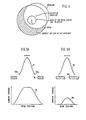
- FIG. 5A illustrates two such problems.
- curve 74 represents the profile of the current density of an electron beam passing through an aperture 76 which is larger than the beam.
- Curve 78 is a plot of the current passing through the aperture as a function of the lateral position of the beam.
- the objective of an alignment servo is to keep the beam centered over the aperture; however, in Fig. 5A, there is a considerable dead band where the beam must be moved laterally some distance before a tail of the beam current strikes the edge of the aperture.
- the prior art incremental servo which makes several small moves and tests, will have to move the beam through several increments before a decrease in current through the aperture is detected.
- the amplitude of the dither is chosen large enough so that the tails of the beam always strike the sides of the aperture, whereby the center of the aperture is immediately determined.
- curve 80 represents the profile of the current density of the electron beam passing through an aperture 82 which is smaller than the beam
- curve 84 is a plot of the current through the aperture as a function of the lateral position of the beam.
- the increment-and-test type of alignment servo performs better for the situation of Fig. 5B than for that of Fig. 5A, but in the region of best alignment there is an area where the change in beam current is very sensitive to small changes in position. Such a small change in a noisy background can cause errors in the alignment servo.
- the present invention uses a dither having an amplitude that is large enough to move the beam out to a position where the current through the aperture vs. position is steeper, so that a more accurate and repeatable determination of the best alignment position can be made.
Landscapes
- Chemical & Material Sciences (AREA)
- Analytical Chemistry (AREA)
- Electron Beam Exposure (AREA)
- Electron Sources, Ion Sources (AREA)
Applications Claiming Priority (2)
| Application Number | Priority Date | Filing Date | Title |
|---|---|---|---|
| US06/507,638 US4568861A (en) | 1983-06-27 | 1983-06-27 | Method and apparatus for controlling alignment and brightness of an electron beam |
| US507638 | 1983-06-27 |
Publications (2)
| Publication Number | Publication Date |
|---|---|
| EP0131699A1 EP0131699A1 (en) | 1985-01-23 |
| EP0131699B1 true EP0131699B1 (en) | 1988-01-27 |
Family
ID=24019506
Family Applications (1)
| Application Number | Title | Priority Date | Filing Date |
|---|---|---|---|
| EP84104924A Expired EP0131699B1 (en) | 1983-06-27 | 1984-05-03 | Method and apparatus for controlling alignment and brightness of an electron beam |
Country Status (4)
| Country | Link |
|---|---|
| US (1) | US4568861A (enExample) |
| EP (1) | EP0131699B1 (enExample) |
| JP (1) | JPS6010720A (enExample) |
| DE (1) | DE3469100D1 (enExample) |
Families Citing this family (12)
| Publication number | Priority date | Publication date | Assignee | Title |
|---|---|---|---|---|
| GB8428198D0 (en) * | 1984-11-08 | 1984-12-19 | Adwel Ltd | Motor monitor synchronisation system |
| US4821196A (en) * | 1987-02-20 | 1989-04-11 | International Business Machines Corporation | High resolution automatic focus correction electronic subsystem for E-beam lithography |
| EP0330763A1 (en) * | 1988-03-03 | 1989-09-06 | Koninklijke Philips Electronics N.V. | Charged particle apparatus with automatic beam set-up |
| DE58907191D1 (de) * | 1989-02-09 | 1994-04-14 | Balzers Hochvakuum | Verfahren zum Zentrieren eines Elektronenstrahles. |
| CA1308203C (en) * | 1989-06-01 | 1992-09-29 | Nanoquest (Canada) Inc. | Magnification compensation apparatus |
| RU2019881C1 (ru) * | 1991-12-26 | 1994-09-15 | Физический институт им.П.Н.Лебедева РАН | Электронно-лучевая трубка |
| JP3272820B2 (ja) * | 1993-06-24 | 2002-04-08 | 富士通株式会社 | 電子ビーム露光装置及び方法 |
| KR0147862B1 (ko) * | 1994-08-25 | 1998-09-15 | 김광호 | 다중모드 모니터의 자동 빔전류 조성회로 및 그 방법 |
| US6145438A (en) * | 1998-03-20 | 2000-11-14 | Berglund; C. Neil | Method and apparatus for direct writing of semiconductor die using microcolumn array |
| US6262425B1 (en) * | 1999-03-11 | 2001-07-17 | International Business Machines Corporation | Curvilinear axis set-up for charged particle lithography |
| US6456019B1 (en) | 2001-02-03 | 2002-09-24 | Nikon Corporation | Real time measurement of leakage current in high voltage electron guns |
| JP7411521B2 (ja) * | 2020-09-03 | 2024-01-11 | 株式会社ニューフレアテクノロジー | 荷電粒子ビーム調整方法、荷電粒子ビーム描画方法、および荷電粒子ビーム照射装置 |
Family Cites Families (7)
| Publication number | Priority date | Publication date | Assignee | Title |
|---|---|---|---|---|
| US3699304A (en) * | 1969-12-15 | 1972-10-17 | Ibm | Electron beam deflection control method and apparatus |
| DE2117193A1 (de) * | 1971-04-08 | 1972-10-12 | Licentia Gmbh | Anordnung zur Feinpositionierung eines Elektronenstrahles |
| US3894271A (en) * | 1973-08-31 | 1975-07-08 | Ibm | Method and apparatus for aligning electron beams |
| US4000440A (en) * | 1974-07-26 | 1976-12-28 | International Business Machines Corporation | Method and apparatus for controlling brightness and alignment of a beam of charged particles |
| JPS5472980A (en) * | 1977-11-24 | 1979-06-11 | Hitachi Ltd | Electron-beam drawing unit |
| JPS5840820B2 (ja) * | 1978-04-28 | 1983-09-08 | 株式会社日立製作所 | 電子ビ−ム自動軸調整装置 |
| JPS5572807A (en) * | 1978-11-27 | 1980-06-02 | Hitachi Ltd | Electron-beam mask check unit |
-
1983
- 1983-06-27 US US06/507,638 patent/US4568861A/en not_active Expired - Lifetime
-
1984
- 1984-05-03 DE DE8484104924T patent/DE3469100D1/de not_active Expired
- 1984-05-03 EP EP84104924A patent/EP0131699B1/en not_active Expired
- 1984-05-17 JP JP59097642A patent/JPS6010720A/ja active Granted
Non-Patent Citations (3)
| Title |
|---|
| "Electron Optics" O. Klemperex, 1972, p. 360 * |
| IBM JOURNAL OF RESEARCH AND DEVELOPMENT, vol. 21, no. 6, November 1977 MAUER "Electron Optics of an Electron-Beam Lithographic System" pages 514-521 * |
| IBM TECHNICAL DISCLOSURE BULLETIN, vol. 19, no. 2, July 1976 LANDON "Gun Servo Alignment for an Electronic-Beam Microfabrication System" pages 464, 465 * |
Also Published As
| Publication number | Publication date |
|---|---|
| EP0131699A1 (en) | 1985-01-23 |
| JPS6010720A (ja) | 1985-01-19 |
| US4568861A (en) | 1986-02-04 |
| DE3469100D1 (en) | 1988-03-03 |
| JPH0348649B2 (enExample) | 1991-07-25 |
Similar Documents
| Publication | Publication Date | Title |
|---|---|---|
| US3894271A (en) | Method and apparatus for aligning electron beams | |
| EP0131699B1 (en) | Method and apparatus for controlling alignment and brightness of an electron beam | |
| US3644700A (en) | Method and apparatus for controlling an electron beam | |
| EP0024884B1 (en) | Method of detecting the position of a substrate using an electron beam | |
| US4149085A (en) | Automatic overlay measurements using an electronic beam system as a measurement tool | |
| US4443703A (en) | Method and apparatus of deflection calibration for a charged particle beam exposure apparatus | |
| CA1103813A (en) | Apparatus for electron beam lithography | |
| US5334846A (en) | Correction of charged particle beam exposure deflection by detecting stage position and a position detection mark | |
| KR0185238B1 (ko) | 음극선관제어장치 | |
| US6570155B1 (en) | Bi-directional electron beam scanning apparatus | |
| US5468969A (en) | Method and apparatus for electron beam lithography | |
| US4749907A (en) | Method and apparatus for automatically calibrating a graticuled cathode ray tube | |
| US4854709A (en) | Arrangement for measuring the distance of a marking element on a displaceable body from a reference marking element | |
| US3924156A (en) | Method and system for correcting an aberration of a beam of charged particles | |
| EP0195162B1 (en) | Method and apparatus for calibrating deflection in an oscilloscope | |
| JP3065472B2 (ja) | 荷電粒子ビーム描画装置における矩形ビームのサイズ及び位置決め調整方法 | |
| Miyauchi et al. | Automatic pattern positioning of scanning electron beam exposure | |
| US2792173A (en) | Function generator | |
| GB1597203A (en) | Position setting systems using a scanning beam | |
| JPS5498577A (en) | Correction method for electron beam scanning position | |
| JPH0282515A (ja) | 電子ビーム描画方法 | |
| JP2000223412A (ja) | 荷電粒子ビーム露光装置及び露光方法 | |
| JP2848417B2 (ja) | 荷電粒子ビーム露光装置および露光方法 | |
| JP2618919B2 (ja) | 電子線描画方法及び電子線描画装置 | |
| JPS5742128A (en) | Exposing method by electron beam |
Legal Events
| Date | Code | Title | Description |
|---|---|---|---|
| PUAI | Public reference made under article 153(3) epc to a published international application that has entered the european phase |
Free format text: ORIGINAL CODE: 0009012 |
|
| AK | Designated contracting states |
Designated state(s): DE FR GB IT |
|
| 17P | Request for examination filed |
Effective date: 19841123 |
|
| 17Q | First examination report despatched |
Effective date: 19860206 |
|
| GRAA | (expected) grant |
Free format text: ORIGINAL CODE: 0009210 |
|
| AK | Designated contracting states |
Kind code of ref document: B1 Designated state(s): DE FR GB IT |
|
| REF | Corresponds to: |
Ref document number: 3469100 Country of ref document: DE Date of ref document: 19880303 |
|
| ITF | It: translation for a ep patent filed | ||
| ET | Fr: translation filed | ||
| PLBE | No opposition filed within time limit |
Free format text: ORIGINAL CODE: 0009261 |
|
| STAA | Information on the status of an ep patent application or granted ep patent |
Free format text: STATUS: NO OPPOSITION FILED WITHIN TIME LIMIT |
|
| 26N | No opposition filed | ||
| ITTA | It: last paid annual fee | ||
| PGFP | Annual fee paid to national office [announced via postgrant information from national office to epo] |
Ref country code: GB Payment date: 19940415 Year of fee payment: 11 |
|
| PG25 | Lapsed in a contracting state [announced via postgrant information from national office to epo] |
Ref country code: GB Effective date: 19950503 |
|
| GBPC | Gb: european patent ceased through non-payment of renewal fee |
Effective date: 19950503 |
|
| PGFP | Annual fee paid to national office [announced via postgrant information from national office to epo] |
Ref country code: FR Payment date: 19960507 Year of fee payment: 13 |
|
| PG25 | Lapsed in a contracting state [announced via postgrant information from national office to epo] |
Ref country code: FR Free format text: LAPSE BECAUSE OF NON-PAYMENT OF DUE FEES Effective date: 19980130 |
|
| REG | Reference to a national code |
Ref country code: FR Ref legal event code: ST |
|
| PGFP | Annual fee paid to national office [announced via postgrant information from national office to epo] |
Ref country code: DE Payment date: 19980522 Year of fee payment: 15 |
|
| PG25 | Lapsed in a contracting state [announced via postgrant information from national office to epo] |
Ref country code: DE Free format text: LAPSE BECAUSE OF NON-PAYMENT OF DUE FEES Effective date: 20000301 |