EP0131265B1 - High capacitive multilayer conductive bars - Google Patents
High capacitive multilayer conductive bars Download PDFInfo
- Publication number
- EP0131265B1 EP0131265B1 EP84107859A EP84107859A EP0131265B1 EP 0131265 B1 EP0131265 B1 EP 0131265B1 EP 84107859 A EP84107859 A EP 84107859A EP 84107859 A EP84107859 A EP 84107859A EP 0131265 B1 EP0131265 B1 EP 0131265B1
- Authority
- EP
- European Patent Office
- Prior art keywords
- conductive
- elements
- capacitive
- dielectric
- conductive elements
- Prior art date
- Legal status (The legal status is an assumption and is not a legal conclusion. Google has not performed a legal analysis and makes no representation as to the accuracy of the status listed.)
- Expired - Lifetime
Links
- 229910000679 solder Inorganic materials 0.000 claims abstract description 61
- 239000000463 material Substances 0.000 claims abstract description 39
- 238000000034 method Methods 0.000 claims abstract description 33
- 239000000956 alloy Substances 0.000 claims abstract description 18
- 238000004519 manufacturing process Methods 0.000 claims abstract description 11
- 238000005476 soldering Methods 0.000 claims abstract description 10
- 239000000853 adhesive Substances 0.000 claims description 30
- 230000001070 adhesive effect Effects 0.000 claims description 30
- 238000002844 melting Methods 0.000 claims description 16
- 230000008018 melting Effects 0.000 claims description 16
- 239000000919 ceramic Substances 0.000 claims description 13
- 229920001169 thermoplastic Polymers 0.000 claims description 10
- 229920001187 thermosetting polymer Polymers 0.000 claims description 10
- 239000004416 thermosoftening plastic Substances 0.000 claims description 10
- 229910045601 alloy Inorganic materials 0.000 claims description 4
- 239000011248 coating agent Substances 0.000 claims description 4
- 238000000576 coating method Methods 0.000 claims description 4
- 238000007731 hot pressing Methods 0.000 claims description 4
- 230000001681 protective effect Effects 0.000 claims description 2
- 238000006116 polymerization reaction Methods 0.000 claims 2
- 238000010030 laminating Methods 0.000 claims 1
- 238000009826 distribution Methods 0.000 abstract description 3
- 239000004020 conductor Substances 0.000 description 14
- 239000010410 layer Substances 0.000 description 13
- 239000012790 adhesive layer Substances 0.000 description 6
- 239000003990 capacitor Substances 0.000 description 5
- 229910052751 metal Inorganic materials 0.000 description 5
- 239000002184 metal Substances 0.000 description 5
- 230000008569 process Effects 0.000 description 5
- 238000009413 insulation Methods 0.000 description 4
- 125000006850 spacer group Chemical group 0.000 description 4
- 238000003466 welding Methods 0.000 description 4
- 229910002113 barium titanate Inorganic materials 0.000 description 3
- VEALVRVVWBQVSL-UHFFFAOYSA-N strontium titanate Chemical compound [Sr+2].[O-][Ti]([O-])=O VEALVRVVWBQVSL-UHFFFAOYSA-N 0.000 description 3
- 241000531908 Aramides Species 0.000 description 2
- 229910001369 Brass Inorganic materials 0.000 description 2
- RYGMFSIKBFXOCR-UHFFFAOYSA-N Copper Chemical compound [Cu] RYGMFSIKBFXOCR-UHFFFAOYSA-N 0.000 description 2
- PXHVJJICTQNCMI-UHFFFAOYSA-N Nickel Chemical compound [Ni] PXHVJJICTQNCMI-UHFFFAOYSA-N 0.000 description 2
- 230000004913 activation Effects 0.000 description 2
- 229920003235 aromatic polyamide Polymers 0.000 description 2
- 229910052788 barium Inorganic materials 0.000 description 2
- DSAJWYNOEDNPEQ-UHFFFAOYSA-N barium atom Chemical compound [Ba] DSAJWYNOEDNPEQ-UHFFFAOYSA-N 0.000 description 2
- 239000011230 binding agent Substances 0.000 description 2
- 239000010951 brass Substances 0.000 description 2
- 229910052802 copper Inorganic materials 0.000 description 2
- 239000010949 copper Substances 0.000 description 2
- 239000003989 dielectric material Substances 0.000 description 2
- 238000005553 drilling Methods 0.000 description 2
- 238000003475 lamination Methods 0.000 description 2
- 239000004033 plastic Substances 0.000 description 2
- 229920003023 plastic Polymers 0.000 description 2
- 229920002620 polyvinyl fluoride Polymers 0.000 description 2
- 239000011347 resin Substances 0.000 description 2
- 229920005989 resin Polymers 0.000 description 2
- 229920002799 BoPET Polymers 0.000 description 1
- 239000005041 Mylar™ Substances 0.000 description 1
- 229920000784 Nomex Polymers 0.000 description 1
- 229910001128 Sn alloy Inorganic materials 0.000 description 1
- 239000004809 Teflon Substances 0.000 description 1
- 229920006362 Teflon® Polymers 0.000 description 1
- NIXOWILDQLNWCW-UHFFFAOYSA-N acrylic acid group Chemical group C(C=C)(=O)O NIXOWILDQLNWCW-UHFFFAOYSA-N 0.000 description 1
- JRPBQTZRNDNNOP-UHFFFAOYSA-N barium titanate Chemical compound [Ba+2].[Ba+2].[O-][Ti]([O-])([O-])[O-] JRPBQTZRNDNNOP-UHFFFAOYSA-N 0.000 description 1
- 238000005219 brazing Methods 0.000 description 1
- 239000002775 capsule Substances 0.000 description 1
- 230000001627 detrimental effect Effects 0.000 description 1
- 238000007598 dipping method Methods 0.000 description 1
- 230000000694 effects Effects 0.000 description 1
- 238000009422 external insulation Methods 0.000 description 1
- 239000000835 fiber Substances 0.000 description 1
- 230000004907 flux Effects 0.000 description 1
- LQBJWKCYZGMFEV-UHFFFAOYSA-N lead tin Chemical compound [Sn].[Pb] LQBJWKCYZGMFEV-UHFFFAOYSA-N 0.000 description 1
- 238000001465 metallisation Methods 0.000 description 1
- 230000004048 modification Effects 0.000 description 1
- 238000012986 modification Methods 0.000 description 1
- 229910052759 nickel Inorganic materials 0.000 description 1
- 239000004763 nomex Substances 0.000 description 1
- 230000003647 oxidation Effects 0.000 description 1
- 238000007254 oxidation reaction Methods 0.000 description 1
- 239000002985 plastic film Substances 0.000 description 1
- 229920003223 poly(pyromellitimide-1,4-diphenyl ether) Polymers 0.000 description 1
- 229920000728 polyester Polymers 0.000 description 1
- 229920006267 polyester film Polymers 0.000 description 1
- 229920001721 polyimide Polymers 0.000 description 1
- 229920001343 polytetrafluoroethylene Polymers 0.000 description 1
- 239000004810 polytetrafluoroethylene Substances 0.000 description 1
- 238000007789 sealing Methods 0.000 description 1
- 229910052709 silver Inorganic materials 0.000 description 1
- 239000004332 silver Substances 0.000 description 1
- 239000002356 single layer Substances 0.000 description 1
- 238000004544 sputter deposition Methods 0.000 description 1
- 239000002344 surface layer Substances 0.000 description 1
- 239000012815 thermoplastic material Substances 0.000 description 1
Images
Classifications
-
- H—ELECTRICITY
- H02—GENERATION; CONVERSION OR DISTRIBUTION OF ELECTRIC POWER
- H02G—INSTALLATION OF ELECTRIC CABLES OR LINES, OR OF COMBINED OPTICAL AND ELECTRIC CABLES OR LINES
- H02G5/00—Installations of bus-bars
- H02G5/005—Laminated bus-bars
-
- H—ELECTRICITY
- H05—ELECTRIC TECHNIQUES NOT OTHERWISE PROVIDED FOR
- H05K—PRINTED CIRCUITS; CASINGS OR CONSTRUCTIONAL DETAILS OF ELECTRIC APPARATUS; MANUFACTURE OF ASSEMBLAGES OF ELECTRICAL COMPONENTS
- H05K1/00—Printed circuits
- H05K1/02—Details
- H05K1/0213—Electrical arrangements not otherwise provided for
- H05K1/0263—High current adaptations, e.g. printed high current conductors or using auxiliary non-printed means; Fine and coarse circuit patterns on one circuit board
-
- Y—GENERAL TAGGING OF NEW TECHNOLOGICAL DEVELOPMENTS; GENERAL TAGGING OF CROSS-SECTIONAL TECHNOLOGIES SPANNING OVER SEVERAL SECTIONS OF THE IPC; TECHNICAL SUBJECTS COVERED BY FORMER USPC CROSS-REFERENCE ART COLLECTIONS [XRACs] AND DIGESTS
- Y10—TECHNICAL SUBJECTS COVERED BY FORMER USPC
- Y10T—TECHNICAL SUBJECTS COVERED BY FORMER US CLASSIFICATION
- Y10T29/00—Metal working
- Y10T29/49—Method of mechanical manufacture
- Y10T29/49002—Electrical device making
- Y10T29/49117—Conductor or circuit manufacturing
- Y10T29/49124—On flat or curved insulated base, e.g., printed circuit, etc.
- Y10T29/49126—Assembling bases
-
- Y—GENERAL TAGGING OF NEW TECHNOLOGICAL DEVELOPMENTS; GENERAL TAGGING OF CROSS-SECTIONAL TECHNOLOGIES SPANNING OVER SEVERAL SECTIONS OF THE IPC; TECHNICAL SUBJECTS COVERED BY FORMER USPC CROSS-REFERENCE ART COLLECTIONS [XRACs] AND DIGESTS
- Y10—TECHNICAL SUBJECTS COVERED BY FORMER USPC
- Y10T—TECHNICAL SUBJECTS COVERED BY FORMER US CLASSIFICATION
- Y10T29/00—Metal working
- Y10T29/49—Method of mechanical manufacture
- Y10T29/49002—Electrical device making
- Y10T29/49117—Conductor or circuit manufacturing
- Y10T29/49194—Assembling elongated conductors, e.g., splicing, etc.
- Y10T29/49201—Assembling elongated conductors, e.g., splicing, etc. with overlapping orienting
Definitions
- the invention relates to a method for manufacturing high capacitive multilayer conductive bars comprising capacitive elements, such as bus bars and to high capacitive multilayer conductive bars obtainable by such method and their use.
- bus bars is herein used for components with wide duty, mainly used for power and/or signal distribution in electronics, for example printed circuits and other high density components.
- the bus bars comprise generally two or more spaced apart conductive elements for feeding the current, usually tinned copper or brass, having a thickness ranging e.g. from about 0.12 mm to about 0.50 mm. They carry a plurality of distribution pins extending therefrom, these pins allowing electrical connections between the conductive elements and the paths of the printed circuit board. In such bus bars, the room between the conductive elements is usually filled with a dielectric for providing a distributed capacitance along the bus bar. So, the bus bar is useful to eliminate transients due to voltage drops and/or to reduce the inherent noise.
- bus bars In prior art bus bars an insulating film or synthetic paper with a thickness usually ranging from 25 to 125 11m is positioned between the conductive elements.
- Suitable dielectrics are PTFE film ("Teflon”), aramide dielectric paper (e.g. "Nomex”), polyester film (e.g. "Mylar”), polyimid film (e.g. "Kapton”) and PVF film (e.g. "Tedlar”). Their relative dielectric constants range from 2 to 9. Bus bars of this type have relatively low capacitance.
- the capacitance per square unit of the bus bar is proportional to the dielectric constant and inversely proportional to the thickness of the dielectric. Reducing the thickness for increasing the capacitance is limited because of the dielectric strength of the material. Higher capacitance at same thickness can be reached with dielectrics having a higher relative dielectric constant.
- Ceramic chips have been used for improving the dielectric constant. They reach dielectric constant values much higher than those above mentioned. Particularly, with barium or strontium titanate ceramics it has been possible to have relative dielectric constants reaching values of 100,000 and more. These chips, precisely BaTi0 3 (barium titanate) and SrTi0 3 (strontium titanate), are easily available on the market in multilayer or monolayer type. In the second case they can have a parallelepiped shape with very small thickness e.g. 0.2 mm. The major sides, having a width e.g. from 3.5 to 5 mm and a length e.g. from 5 to 35 mm, are metallized by laying a conductive film or by sputtering or the like, whereas the edges are not metallized. These chips are the actual capacitors.
- Metallization is made of silver or nickel or another suitable metal, with usual vacuum laying methods; the metal film has a thickness up to some (..1m providing a continuous conductive layer on the major sides.
- the cross section of the continuous conductive layer on the major sides of the chips can be small, since the layer does not feed the main current, but is mostly crossed by the variable current due to the noise power generated by the active components.
- An appreciable cross section of the conductive layer is, however, useful for keeping the electrical series resistance low and for lowering the equivalent series resistance of the capacitors.
- the metallized ceramic chips are sealed to the outward conductive bars by means of a nonconductive adhesive, while the surfaces of the chips facing the inwardly facing surfaces of the plate bars are provided with a rough finish in order to make electrical contacts between the conductive bar and the metallized layer of the chip.
- Such an electrical connection is, however, uncertain and unreliable either due to some excess amount of adhesive covering the inwardly facing surfaces of the multilayer bus bar assembly, or due to the property of the adhesive-typically a thermoplastic material-which, when heated up to its softening point, starts flowing thus leading the electrical contacts to fail. In any case, it is difficult to select an adequate amount of adhesive.
- the bus bar assembly comprises discrete capacitive elements, e.g. BaTi0 3 having conductive layers e.g. of Ag, which are electrically connected to the bus bar conductors.
- the electrical connection may be established by solder and the conductors may be covered with plastics.
- the bus bar conductors are laminated to an insulating spacer having apertures therein to receive the conductively coated discrete capacitors.
- Printed conductive tracks on the insulating spacer make the connection between the bus conductors and the conductive layers.
- the bus conductors are printed tracks on plastic sheets adhered to an apertured plastic spacer with conductively coated capacitors in the apertures and conductive adhesive between the conductive layers and the bus conductors.
- FR-A-2 458 163 relates to a high-capacitive multilayer conductive bar comprising capacitive elements, dielectric elements and two spaced apart conductive elements.
- the capacitive elements and dielectric elements are mostly covered by a non-conductive binder material except for the upper boarder of the capacitive and dielectric elements.
- the mechanical connection between the conductive elements and the capacitive dielectric elements is established by said binder. According to this known method, this is done in a first step. In a second step, the electrical connection between the conductive elements and the capacitive elements is established by a solder material.
- FR-A-2 458 163 teaches a two- step method for assembling the devices.
- the invention as claimed is intended to provide a simple and economic method for manufacturing high capacitive multilayer conductive bars, in which the required electrical and mechanical connections between the various elements of the bus bars are safe and reliable even under extreme conditions, such as high temperature or mechanical stress. It is another object to provide such bars with relatively low equivalent series resistance of the inner capacitors and great effectiveness in reducing inherent noise.
- the invention is indicated by the features of the independent claims 1,3, 18, 20.
- the advantages provided by the invention consist mainly in that the mechanical and the electrical connections are established in the best form by using two different bonding materials.
- the solder alloy material is used because it is qualified for establishing best electrical connection which is durable and additionally has a low impedance.
- the solder alloy material is used together with a best possible non-conductive bonding material that establishes the mechanical connection, whereby this demand is accomplished in the best manner.
- the non-conductive bonding material may be applied abundantly without disturbing the function of the multilayer conductive bars.
- every space within the conductive bars assembly is preferably filled by the non-conductive bonding material so that the assembly is stable and compact and has a good reliability.
- the conductive, the capacitive and the dielectric elements together with the soldering alloy as well as the non-conductive bonding materials are laminated during a single hot pressing step. Therefore, the solder alloy material is placed between the conductive elements and the intermediate capacitive elements, and the non-conductive bonding material is placed on the surfaces of the various dielectric elements.
- the bonding materials establishing the mechanical and electrical connections are selected in view of similar properties as regards process temperature and/or pressure.
- the non-conductive bonding material is preferably a thermosetting or thermoplastic adhesive, having an activation temperature between about 150°C and 200°C.
- the bonding via the thermoplastic adhesive is preferably performed at a softening temperature of about 150°C.
- the bonding via the thermosetting adhesive is preferably performed at a polymerisation temperature of about 185°C. Both adhesives are suitable materials for adhering metal as well as dielectric.
- the so performed mechanical connection is durable and certain.
- the soldering alloy material is preferably a solder paste, a solder preform material or a preform welding material having a melting point between about 140°C and 200°C, i.e.
- soldering rather than brazing.
- Solder materials usually lead-tin alloys join the metal surfaces of the conductive elements and the capacitive element without melting them. Soldering makes a good electric connection and mechanical connection, too.
- Suitable solders are e.g. SnPbAgSb 62/35.7/2/0.3 class Sn 62, melting point at 179°C, or InPbAg 80/15/5, melting point at 149°C (manufacturer Multicore Solder Ltd., U.K.). These solders are pastes with a viscosity of usually more than 200,000 cP at 25°C. Because of this relatively high viscosity the solder paste is prevented from flowing even at higher operation temperatures.
- thermoplastic adhesive with a softening temperature of about 150°C together with InPbAg solder paste with a melting point of 149°C
- thermosetting adhesive with a polymerisation temperature of 185°C together with SnPbAgSb solder paste with a melting point of 179°C.
- the capacitive elements are preferably metallized ceramic chips whose edges are not electrically conductive. Each metallized major side is facing to the appropriate conductive element. For electrical connection between them the solder alloy material is placed on the metallized sides of the capacitive element and/or the facing sides of the conductive element in a suitable quantity depending on the chip size.
- the solder for instance, is laid by dotting or in a continuous strip in the central zone on both sides of the chips and not less than 1 mm from the edge and/or in the mid area of the conductive elements. Quantity shall be suitable, for instance, 0.02 g per point or 0.1 g per linear cm.
- the chips are preferably placed in the centre of the conductive element.
- solder due to its viscosity, makes positioning of the capacitive element relative to the conductive element easier.
- the small quantity of solder cannot produce any short-circuiting during manufacturing operations, because solder remains within the middle of the capacitive element, well far away from the edges.
- dielectric elements are bonded to the outwardly facing or exposed surfaces of the conductive elements in order to insulate and to capsule the assembly. This external insulation is established during the above mentioned one hot pressing step.
- These outer dielectric elements are preferably a synthetic paper or a film strip.
- Preferably these elements have a dry adhesive layer on the internal sides.
- This thermosetting or thermoplastic adhesive is an acrylic, or epoxyde or polyester adhesive.
- a multilayer conductive bar having one or more isolating layers between the conductive element and the capacitive element.
- This isolating layer preferably an inner dielectric element, is bonded by the non-conductive adhesive to the conductive element and to the capacitive element. Both major sides of the inner dielectric element are covered preferably with a dry adhesive layer.
- This element comprises holes wherethrough electrical contact between the adjacent conductive element and the capacitive element is made by the solder paste or the preform welding material, which may be filled in these holes. The holes having a diameter of about 1 to 3 mm are centered in the mid area of the capacitive element, where the electrical connection should be performed.
- inner dielectric elements when capacitive elements do not fill all the conductive bar length, inner dielectric elements are placed within the empty extremities aside the capacitive elements and are bonded to the inwardly facing surfaces of the conductive elements.
- the bonding may be performed by the same adhesive as used for the outer dielectric elements.
- the adhesive may be a film layer on one or two sides of the dielectric elements.
- the inner dielectric element used as a spacer has the same thickness as the capacitive element and may be a synthetic paper or a film strip.
- the invention also provides a modification of the method by manufacturing the high capacitive multilayer conductive bars in more than one step. For example, firstly soldering the capacitive element to the conductive elements and at the same time bonding the inner dielectric elements to the conductive elements and/or capacitive element, and subsequently externally coating the bonded elements with a protective and isolating material.
- the coating can be made, for instance, by means of epossydic or syliconic resin, by dipping or by an electrostatic system.
- High capacitance bus bars are useful in many applications. They are especially designed to fit under integrated circuits to save space and to feed the supplying current to the integrated circuits and/or to establish an electrical connection between two or more integrated circuits.
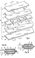
- bus bar 10 consists of ceramic chips 12 laid between the conductors 14 and 16, external dielectric elements 18 and 20 each one with thermosetting or thermoplastic dry adhesive 22 and 24. Said dry adhesive layers 22 and 24 after assembling shall be connected with the external side of the conductors 14 and 16. In the case that the external coating is made separately an epoxydic or siliconic resin is laid on said conductors.
- Barium or strontium titanate ceramic chips 12 are metallized on their major sides, the metal layer 12' being provided by well known methods.
- Spacing dielectric 13 and its dry adhesive 13' are placed on the empty sides of the bus bar between said conductors.
- a suitable quantity of the solder paste is placed on the metallized surfaces 12' of the capacitive elements 12 and/or on the internal side of the conductive elements 14 and 16.
- the conductive bars 14 and 16 are preferably made from tinned copper and/or brass with some pins 32 serving as a connection to the external circuitry.
- the bus bar 10 can be provided directly with external dielectric elements 18 and 20 and thermosetting and thermoplastic dry adhesive 22 and 24.
- the bar 10 can be assembled together during one hot pressing step.
- the multilayer conductive bar is assembled altogether and it looks like a "sandwich".
- the inner dielectric element 13 having dry adhesive surface layers 13'.
- the whole is covered from the outer dielectric elements 18, 20 which are mechanically connected to the conductive elements 14, 16 by the adhesive layers 22, 24. Every space within the conductive bars assembly is filled with the same adhesive.
- the capacitive element 12 In the middle of the assembly there is shown the capacitive element 12 with the metallic surfaces 12' (Fig. 2b).
- the electrical connection is established by the solder 30 between the major sides of the capacitive element 12 and the conductive elements, which are positioned under and above the capacitive element 12.
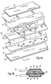
- the other components correspond to those of Fig. 2a.
- the insulation between every chip inside the bus bar can be increased by using an inner dielectric element 113 which is a bit longer than the conductive elements.
- This inner dielectric element 113 having dry adhesive layers 113' on each major side comprises holes 31.
- the solder 30 is placed on the capacitive element 12 having metallized surfaces 12' in the mid area of the major sides and/or on the inwardly facing surfaces of the conductors in the positions corresponding to the holes.
- the holes 31 of the inner dielectric element 113 are adjusted to the mid area of the capacitive elements. So that electrical connection is made by solder through the holes between the conductive element 16 and the capacitive element 12.
- On top and base of the exploded view are shown the outer dielectric elements 18, 20 with the inwardly facing dry adhesive layers 22, 24, respectively.
- the bar according to Fig. 3b comprises an additional inner dielectric element 113 between the capacitive element 12 and the conductive element 16.
- the solder 30 connects the capacitive element 12 through the inner dielectric element hole with the conductive element 16.
- the contact between the metallized ceramic chips and the conductor implies dielectric strip drilling, one or more holes 31 per chip centre (diameter 1 to 3 mm) care shall be taken to avoid drilling where there is no chip.
- the dielectric strips are by 1 or 2 mm wider than the conductive element, they have a thickness of usually 50 11 m; the thicker they are, the better insulation is requested.
- the strip material shall give a good insulation up to at least 150°C, or even up to 200°C, it can be a film, or aramide fiber.
- the adhesive can be thermosetting or thermoplastic material, the activation temperature can be between about 150°C and 200°C.
- the drilled dielectric strip is placed on the first conductor already lying in the lamination die, in each hole shall be put 10 mg of solder paste to fill it sufficiently.
- solder paste for instance, is SnPbAgSb 62/35.7/2/0.3 (manufacturer Multicore Solders Ltd., U.K.), with a melting point at 179°C, non activated flux type R or type Xersin 2000 or similar with best insulation quality.
- Another solder paste can be InPbAg 80/15/5 from same producer, with a melting point at 140°C.
- a solder preform can be used.
- the preform element shall be big enough to provide welding in all the sections of the whole square element, for instance, 1.5x1.5x0.2 mm without causing excess of melting material during the sealing of the component. In this case the solder flow can be avoided. Then the ceramic chips are laid on the holes filled with solder. The chips and the relative holes can be placed in the centre of the bar or can be uniformly distributed all along the bar, in the second case a better uniformity in electrical parameters is achieved.
- solder paste or preform welding is laid on the other metallized side of the chip, of the same type and quantity as above, always along the major axis. Solder leaking after melting shall be avoided.
- solder materials are indicative, other materials may be used if their characteristics are the same.
Landscapes
- Fixed Capacitors And Capacitor Manufacturing Machines (AREA)
- Insulated Conductors (AREA)
- Pressure Welding/Diffusion-Bonding (AREA)
- Coating With Molten Metal (AREA)
- Manufacturing Of Electrical Connectors (AREA)
- Superconductors And Manufacturing Methods Therefor (AREA)
- Linear Motors (AREA)
- Laminated Bodies (AREA)
Priority Applications (1)
| Application Number | Priority Date | Filing Date | Title |
|---|---|---|---|
| AT84107859T ATE52641T1 (de) | 1983-07-06 | 1984-07-05 | Mehrschichtige leitende schienen hoher kapazitaet. |
Applications Claiming Priority (2)
| Application Number | Priority Date | Filing Date | Title |
|---|---|---|---|
| IT2195483 | 1983-07-06 | ||
| IT21954/83A IT1194301B (it) | 1983-07-06 | 1983-07-06 | Metodo per la fabbricazioni ad alta capacita' con connessioni elettriche ottenute per la saldatura,e relative barre prodotte secondo tale metodo |
Publications (3)
| Publication Number | Publication Date |
|---|---|
| EP0131265A2 EP0131265A2 (en) | 1985-01-16 |
| EP0131265A3 EP0131265A3 (en) | 1986-08-20 |
| EP0131265B1 true EP0131265B1 (en) | 1990-05-09 |
Family
ID=11189344
Family Applications (1)
| Application Number | Title | Priority Date | Filing Date |
|---|---|---|---|
| EP84107859A Expired - Lifetime EP0131265B1 (en) | 1983-07-06 | 1984-07-05 | High capacitive multilayer conductive bars |
Country Status (6)
| Country | Link |
|---|---|
| US (1) | US4584768A (cg-RX-API-DMAC7.html) |
| EP (1) | EP0131265B1 (cg-RX-API-DMAC7.html) |
| JP (1) | JPS6037610A (cg-RX-API-DMAC7.html) |
| AT (1) | ATE52641T1 (cg-RX-API-DMAC7.html) |
| DE (2) | DE3482227D1 (cg-RX-API-DMAC7.html) |
| IT (1) | IT1194301B (cg-RX-API-DMAC7.html) |
Families Citing this family (27)
| Publication number | Priority date | Publication date | Assignee | Title |
|---|---|---|---|---|
| US5166867A (en) * | 1985-12-31 | 1992-11-24 | Fujitsu Limited | Bus bar for a circuit board |
| US4878155A (en) * | 1987-09-25 | 1989-10-31 | Conley Larry R | High speed discrete wire pin panel assembly with embedded capacitors |
| US6498546B1 (en) * | 2000-08-25 | 2002-12-24 | James Leych Lau | Utilization of proximity effect in ripple noise filtering |
| DE102005044392A1 (de) * | 2005-09-16 | 2007-03-29 | Siemens Ag | Piezoaktor mit verbesserter Verbindung zwischen Aktorkörper und Kontaktstift |
| KR100731293B1 (ko) * | 2006-02-24 | 2007-06-27 | 경신공업 주식회사 | 버스 바의 전기접속부 제조방법 및 제조장치 |
| WO2008101067A1 (en) * | 2007-02-16 | 2008-08-21 | World Properties, Inc. | Laminated bus bars and methods of manufacture thereof |
| JP4905254B2 (ja) * | 2007-05-25 | 2012-03-28 | トヨタ自動車株式会社 | コンデンサ一体バスバーの製造方法 |
| JP2009076320A (ja) * | 2007-09-20 | 2009-04-09 | Yaskawa Electric Corp | 積層バスバー回路板の製造装置および製造方法、これによって製造されるバスバー、電力変換装置 |
| US20100239899A1 (en) * | 2009-03-23 | 2010-09-23 | Joe Brown | Gauntlet motive battery |
| US9979173B2 (en) * | 2011-04-29 | 2018-05-22 | Ge Energy Power Conversion Technology Limited | Bus bar assembly and method of manufacturing same |
| DE102016206459B3 (de) * | 2016-04-18 | 2017-10-05 | Continental Automotive Gmbh | Kombination, umfassend ein Gehäuse und einen Flansch, und Anordnung |
| FR3065575B1 (fr) * | 2017-04-20 | 2020-02-21 | Auxel | Fabrication d'un dispositif a plaques conductrices |
| JP6618504B2 (ja) * | 2017-04-28 | 2019-12-11 | 矢崎総業株式会社 | バスバー及びバスバーの製造方法 |
| US10850623B2 (en) | 2017-10-30 | 2020-12-01 | Sf Motors, Inc. | Stacked electric vehicle inverter cells |
| US10790758B2 (en) | 2018-03-08 | 2020-09-29 | Chongqing Jinkang New Energy Vehicle Co., Ltd. | Power converter for electric vehicle drive systems |
| US10236791B1 (en) | 2018-03-23 | 2019-03-19 | Sf Motors, Inc. | Inverter module having multiple half-bridge modules for a power converter of an electric vehicle |
| US10779445B2 (en) | 2018-03-23 | 2020-09-15 | Chongqing Jinkang New Energy Vehicle Co., Ltd. | Inverter module having multiple half-bridge modules for a power converter of an electric vehicle |
| US10756649B2 (en) | 2018-03-23 | 2020-08-25 | Chongqing Jinkang New Energy Vehicle Co., Ltd. | Inverter module having multiple half-bridge modules for a power converter of an electric vehicle |
| US10778117B2 (en) | 2018-04-17 | 2020-09-15 | Chongqing Jinkang New Energy Vehicle Co., Ltd. | Inverter module of an electric vehicle |
| US10772242B2 (en) | 2018-04-17 | 2020-09-08 | Chongqing Jinkang New Energy Vehicle Co., Ltd. | Inverter module of an electric vehicle |
| US10600578B2 (en) | 2018-04-26 | 2020-03-24 | Sf Motors, Inc. | Electric vehicle inverter module capacitors |
| US10600577B2 (en) | 2018-04-26 | 2020-03-24 | Sf Motors, Inc. | Electric vehicle inverter module capacitors |
| US10660242B2 (en) | 2018-04-26 | 2020-05-19 | Chongqing Jinkang New Energy Vehicle Co., Ltd. | Electric vehicle inverter module heat sink |
| US10608423B2 (en) * | 2018-04-26 | 2020-03-31 | Sf Motors, Inc. | Electric vehicle inverter module laminated bus bar |
| US10998706B2 (en) * | 2019-10-08 | 2021-05-04 | Hamilton Sundstrand Corporation | Laminated bus bars |
| US11832390B2 (en) | 2022-03-07 | 2023-11-28 | Rolls-Royce Corporation | Multilayer copper bus bars with soldered through hole components |
| US11876364B2 (en) | 2022-03-07 | 2024-01-16 | Rolls-Royce Corporation | Multilayer electronic components with soldered through holes |
Family Cites Families (14)
| Publication number | Priority date | Publication date | Assignee | Title |
|---|---|---|---|---|
| JPS6021451B2 (ja) * | 1977-10-08 | 1985-05-28 | 日本メクトロン株式会社 | コンデンサ内蔵型積層母線 |
| US4236046A (en) * | 1978-10-10 | 1980-11-25 | Rogers Corporation | High capacitance bus bar |
| JPS5566335U (cg-RX-API-DMAC7.html) * | 1978-10-31 | 1980-05-07 | ||
| JPS55111328U (cg-RX-API-DMAC7.html) * | 1979-01-29 | 1980-08-05 | ||
| JPS55160417A (en) * | 1979-05-31 | 1980-12-13 | Nippon Mektron Kk | Capacitor internally containing laminate bus and method of fabricating same |
| US4236038A (en) * | 1979-07-19 | 1980-11-25 | Rogers Corporation | High capacitance multilayer bus bar and method of manufacture thereof |
| US4420653A (en) * | 1980-05-29 | 1983-12-13 | Rogers Corporation | High capacitance bus bar and method of manufacture thereof |
| US4440972A (en) * | 1981-03-31 | 1984-04-03 | Rogers Corporation | Miniaturized bus bar with capacitors and method of making same |
| US4394532A (en) * | 1981-03-31 | 1983-07-19 | Rogers Corporation | Multilayer current distribution systems and methods of fabrication thereof |
| US4399321A (en) * | 1981-03-31 | 1983-08-16 | Rogers Corporation | High capacitance bus bar including multilayer ceramic capacitors |
| US4436953A (en) * | 1981-03-31 | 1984-03-13 | Rogers Corporation | Bus bar assembly with discrete capacitor elements |
| US4381423A (en) * | 1981-03-31 | 1983-04-26 | Rogers Corporation | High capacitance bus bar manufacturing technique |
| US4430522A (en) * | 1982-07-16 | 1984-02-07 | Eldre Components, Inc. | Laminated bus bar with capacitors and method of making same |
| US4515304A (en) * | 1982-09-27 | 1985-05-07 | Northern Telecom Limited | Mounting of electronic components on printed circuit boards |
-
1983
- 1983-07-06 IT IT21954/83A patent/IT1194301B/it active
-
1984
- 1984-07-03 US US06/627,349 patent/US4584768A/en not_active Expired - Fee Related
- 1984-07-05 DE DE8484107859T patent/DE3482227D1/de not_active Expired - Fee Related
- 1984-07-05 JP JP59139734A patent/JPS6037610A/ja active Granted
- 1984-07-05 EP EP84107859A patent/EP0131265B1/en not_active Expired - Lifetime
- 1984-07-05 DE DE198484107859T patent/DE131265T1/de active Pending
- 1984-07-05 AT AT84107859T patent/ATE52641T1/de not_active IP Right Cessation
Also Published As
| Publication number | Publication date |
|---|---|
| DE3482227D1 (de) | 1990-06-13 |
| EP0131265A3 (en) | 1986-08-20 |
| ATE52641T1 (de) | 1990-05-15 |
| JPH0572041B2 (cg-RX-API-DMAC7.html) | 1993-10-08 |
| US4584768A (en) | 1986-04-29 |
| DE131265T1 (de) | 1985-08-14 |
| IT1194301B (it) | 1988-09-14 |
| EP0131265A2 (en) | 1985-01-16 |
| IT8321954A1 (it) | 1985-01-06 |
| IT8321954A0 (it) | 1983-07-06 |
| JPS6037610A (ja) | 1985-02-27 |
Similar Documents
| Publication | Publication Date | Title |
|---|---|---|
| EP0131265B1 (en) | High capacitive multilayer conductive bars | |
| US4496793A (en) | Multi-layer metal core circuit board laminate with a controlled thermal coefficient of expansion | |
| US6768061B2 (en) | Multilayer circuit board | |
| US6020808A (en) | Multilayer conductive polymer positive temperature coefficent device | |
| KR940009175B1 (ko) | 다층 프린트기판의 제조방법 | |
| JP3363651B2 (ja) | プリント配線板およびその設計方法 | |
| US6812412B2 (en) | Multi-layer wiring board and method of producing same | |
| KR100412155B1 (ko) | 전자 부품 장치 및 그의 제조방법 | |
| EP0446656A1 (en) | Method of manufacturing a multilayer circuit board | |
| US5073840A (en) | Circuit board with coated metal support structure and method for making same | |
| KR20200001521A (ko) | 적층 세라믹 전자부품 | |
| KR20010072571A (ko) | 전기 장치 | |
| US20060176675A1 (en) | Multi-layer polymeric electronic device and method of manufacturing same | |
| EP1414281A1 (en) | Circuit module | |
| US6534842B2 (en) | Composite components and the method of manufacturing the same | |
| CA1218123A (en) | High capacitance laminated buss and method of manufacture | |
| US20040011855A1 (en) | Method for producing multilayer wiring circuit board | |
| US5185690A (en) | High dielectric constant sheet material | |
| US5440802A (en) | Method of making wire element ceramic chip fuses | |
| US12057274B2 (en) | Packaging structures for electronic elements and solid electrolytic capacitor elements and methods thereof | |
| JP2004119483A (ja) | 素子内蔵基板 | |
| US12057275B2 (en) | Packaging of roll-type solid electrolytic capacitor elements | |
| GB2080729A (en) | A multi-layer metal core circuit board laminate with a controlled thermal coefficient of expansion and method for making same. | |
| JPS5844789A (ja) | プリント配線板に誘電体を形成する方法 | |
| JP2003324280A (ja) | プリント基板の製造方法 |
Legal Events
| Date | Code | Title | Description |
|---|---|---|---|
| PUAI | Public reference made under article 153(3) epc to a published international application that has entered the european phase |
Free format text: ORIGINAL CODE: 0009012 |
|
| AK | Designated contracting states |
Designated state(s): AT BE CH DE FR GB IT LI LU NL SE |
|
| TCAT | At: translation of patent claims filed | ||
| ITCL | It: translation for ep claims filed |
Representative=s name: STUDIO LUNATI & MAZZONI S.A.S |
|
| EL | Fr: translation of claims filed | ||
| DET | De: translation of patent claims | ||
| PUAL | Search report despatched |
Free format text: ORIGINAL CODE: 0009013 |
|
| AK | Designated contracting states |
Kind code of ref document: A3 Designated state(s): AT BE CH DE FR GB IT LI LU NL SE |
|
| 17P | Request for examination filed |
Effective date: 19860925 |
|
| 17Q | First examination report despatched |
Effective date: 19880422 |
|
| GRAA | (expected) grant |
Free format text: ORIGINAL CODE: 0009210 |
|
| AK | Designated contracting states |
Kind code of ref document: B1 Designated state(s): AT BE CH DE FR GB IT LI LU NL SE |
|
| PG25 | Lapsed in a contracting state [announced via postgrant information from national office to epo] |
Ref country code: SE Effective date: 19900509 Ref country code: NL Effective date: 19900509 Ref country code: LI Effective date: 19900509 Ref country code: IT Free format text: LAPSE BECAUSE OF FAILURE TO SUBMIT A TRANSLATION OF THE DESCRIPTION OR TO PAY THE FEE WITHIN THE PRESCRIBED TIME-LIMIT;WARNING: LAPSES OF ITALIAN PATENTS WITH EFFECTIVE DATE BEFORE 2007 MAY HAVE OCCURRED AT ANY TIME BEFORE 2007. THE CORRECT EFFECTIVE DATE MAY BE DIFFERENT FROM THE ONE RECORDED. Effective date: 19900509 Ref country code: CH Effective date: 19900509 Ref country code: BE Effective date: 19900509 Ref country code: AT Effective date: 19900509 |
|
| REF | Corresponds to: |
Ref document number: 52641 Country of ref document: AT Date of ref document: 19900515 Kind code of ref document: T |
|
| REF | Corresponds to: |
Ref document number: 3482227 Country of ref document: DE Date of ref document: 19900613 |
|
| ET | Fr: translation filed | ||
| PGFP | Annual fee paid to national office [announced via postgrant information from national office to epo] |
Ref country code: GB Payment date: 19900625 Year of fee payment: 7 |
|
| PGFP | Annual fee paid to national office [announced via postgrant information from national office to epo] |
Ref country code: FR Payment date: 19900717 Year of fee payment: 7 |
|
| PG25 | Lapsed in a contracting state [announced via postgrant information from national office to epo] |
Ref country code: LU Free format text: LAPSE BECAUSE OF NON-PAYMENT OF DUE FEES Effective date: 19900731 |
|
| REG | Reference to a national code |
Ref country code: CH Ref legal event code: PL |
|
| PGFP | Annual fee paid to national office [announced via postgrant information from national office to epo] |
Ref country code: DE Payment date: 19900927 Year of fee payment: 7 |
|
| NLV1 | Nl: lapsed or annulled due to failure to fulfill the requirements of art. 29p and 29m of the patents act | ||
| PLBE | No opposition filed within time limit |
Free format text: ORIGINAL CODE: 0009261 |
|
| STAA | Information on the status of an ep patent application or granted ep patent |
Free format text: STATUS: NO OPPOSITION FILED WITHIN TIME LIMIT |
|
| 26N | No opposition filed | ||
| PG25 | Lapsed in a contracting state [announced via postgrant information from national office to epo] |
Ref country code: GB Effective date: 19910705 |
|
| GBPC | Gb: european patent ceased through non-payment of renewal fee | ||
| PG25 | Lapsed in a contracting state [announced via postgrant information from national office to epo] |
Ref country code: FR Effective date: 19920331 |
|
| PG25 | Lapsed in a contracting state [announced via postgrant information from national office to epo] |
Ref country code: DE Effective date: 19920401 |
|
| REG | Reference to a national code |
Ref country code: FR Ref legal event code: ST |