EP0130497A2 - Technique d'alignement pour un faisceau de balayage - Google Patents
Technique d'alignement pour un faisceau de balayage Download PDFInfo
- Publication number
- EP0130497A2 EP0130497A2 EP84107152A EP84107152A EP0130497A2 EP 0130497 A2 EP0130497 A2 EP 0130497A2 EP 84107152 A EP84107152 A EP 84107152A EP 84107152 A EP84107152 A EP 84107152A EP 0130497 A2 EP0130497 A2 EP 0130497A2
- Authority
- EP
- European Patent Office
- Prior art keywords
- correction
- signal
- scan
- scanning
- position correction
- Prior art date
- Legal status (The legal status is an assumption and is not a legal conclusion. Google has not performed a legal analysis and makes no representation as to the accuracy of the status listed.)
- Granted
Links
- 238000000034 method Methods 0.000 title abstract description 27
- 238000012937 correction Methods 0.000 claims abstract description 136
- 238000012545 processing Methods 0.000 claims description 3
- 239000002184 metal Substances 0.000 abstract description 6
- 230000035945 sensitivity Effects 0.000 abstract description 6
- 238000007689 inspection Methods 0.000 abstract description 5
- 239000011521 glass Substances 0.000 abstract description 4
- 239000000463 material Substances 0.000 description 8
- 238000010586 diagram Methods 0.000 description 7
- 238000010894 electron beam technology Methods 0.000 description 7
- 239000000523 sample Substances 0.000 description 6
- 239000000758 substrate Substances 0.000 description 5
- 238000013459 approach Methods 0.000 description 4
- 238000005516 engineering process Methods 0.000 description 4
- 230000000694 effects Effects 0.000 description 3
- 238000010420 art technique Methods 0.000 description 2
- 239000002872 contrast media Substances 0.000 description 2
- 238000005259 measurement Methods 0.000 description 2
- 238000013519 translation Methods 0.000 description 2
- 238000000576 coating method Methods 0.000 description 1
- 230000007812 deficiency Effects 0.000 description 1
- 238000001514 detection method Methods 0.000 description 1
- 238000000609 electron-beam lithography Methods 0.000 description 1
- 230000010354 integration Effects 0.000 description 1
- 238000004519 manufacturing process Methods 0.000 description 1
- 238000001465 metallisation Methods 0.000 description 1
- 238000012986 modification Methods 0.000 description 1
- 230000004048 modification Effects 0.000 description 1
- 230000003287 optical effect Effects 0.000 description 1
- 238000012360 testing method Methods 0.000 description 1
- 238000012795 verification Methods 0.000 description 1
Images


Classifications
-
- H—ELECTRICITY
- H01—ELECTRIC ELEMENTS
- H01J—ELECTRIC DISCHARGE TUBES OR DISCHARGE LAMPS
- H01J37/00—Discharge tubes with provision for introducing objects or material to be exposed to the discharge, e.g. for the purpose of examination or processing thereof
- H01J37/30—Electron-beam or ion-beam tubes for localised treatment of objects
- H01J37/304—Controlling tubes by information coming from the objects or from the beam, e.g. correction signals
- H01J37/3045—Object or beam position registration
-
- H—ELECTRICITY
- H01—ELECTRIC ELEMENTS
- H01L—SEMICONDUCTOR DEVICES NOT COVERED BY CLASS H10
- H01L23/00—Details of semiconductor or other solid state devices
- H01L23/544—Marks applied to semiconductor devices or parts, e.g. registration marks, alignment structures, wafer maps
-
- H—ELECTRICITY
- H01—ELECTRIC ELEMENTS
- H01L—SEMICONDUCTOR DEVICES NOT COVERED BY CLASS H10
- H01L2223/00—Details relating to semiconductor or other solid state devices covered by the group H01L23/00
- H01L2223/544—Marks applied to semiconductor devices or parts
- H01L2223/54453—Marks applied to semiconductor devices or parts for use prior to dicing
-
- H—ELECTRICITY
- H01—ELECTRIC ELEMENTS
- H01L—SEMICONDUCTOR DEVICES NOT COVERED BY CLASS H10
- H01L2924/00—Indexing scheme for arrangements or methods for connecting or disconnecting semiconductor or solid-state bodies as covered by H01L24/00
- H01L2924/0001—Technical content checked by a classifier
- H01L2924/0002—Not covered by any one of groups H01L24/00, H01L24/00 and H01L2224/00
Definitions
- This invention relates to an automatic beam alignment system for testing, measurement, and verification of high contrast image patterns.
- Registration is required to correct for a lack of overlay between a scanning beam and target features. This misalignment results from target fabrication and beam deflection tolerances. Tolerances for each are small over short distances but are significant over the deflection range of the inspection tool.
- Known registration techniques may employ the measurement of either transmitted or reflected light, reflected or secondary electrons, or backscattered currents when a controllable beam is selectively addressed onto the unit to be inspected with controlled alignment. Reference is made to "Registration Mark Detection For Electron Beam Lithography-EL-1 Systems", Davis, IBM J. Res. Dev., Vol. 25, No. 5, pp. 545-553, September 1980. Davis examines various techniques of automatic wafer registration in E-beam lithography. This is used to locate differences in surface topology as distinguished from differences in materials.
- the difference between integrated signals resulting from scanning equal areas straddling opposite sides of features is a correction signal having a polarity related to the direction and an amplitude proportional to the magnitude of the beam-to-feature translation error.
- U.S. patents 4,301,370; 4,238,780; 4,209,830; and 4,203,064 all relate to techniques for aligning integrated circuit chips for purposes of bonding.
- U.S. patent 3,670,153 relates to a technique for aligning substrates prior to applying the chips bor bonding.
- U.S. patent 3,924,113 relates to a technique of aligning an electron beam scanned field to a wafer.
- U.S. patents 3,955,072; 4,052,603; and 4,103,998 relate to optical mask to wafer alignment techniques.
- U.S. patent 3,876,883 relates to a system for aligning a mask to a wafer in an electron beam projection system. These prior art devices determine the relationship of superimposed images of pairs of known features on two objects, that is the mask and wafer, to provide mutual alignment. No attempt is made in these systems to align the objects to a scanning beam.
- U.S. patent 3,575,588 describes a technique for writing wiring patterns on substrates with an electron beam. In accordance with this patent the amount of data required for control of the beam sweep and deflection is reduced. Alignment is not a part of this technology.
- Known registration techniques therefore commence by scanning features and generating a correction value which is then applied.
- registration sensitivity is inversely proportional to the width (W) of the areas scanned for registration, i.e. scan windows. Consequently, minimizing the value of W is an important criterion in any system.
- the minimum value of W is determined by the capture range (C) required to insure registration over the range of the mask and the electron beam deflection tolerances. As such, W > 2C.
- Yet another object of this invention is to define a system of registration which eliminates the effect of backscattered current variations.
- the detector output signal While scanning such that the beam straddles the edge of a feature, the detector output signal will approach the high contrast signal level as more and more of the electron beam impinges on the high contrast area of the target. Conversely, the signal will approach the low contrast signal level as more of the beam impinges on the low contrast area.
- the present invention allows the use of minimum width (W) scan windows in the registration process to increase registration sensitivity.
- Prior art techniques have utilized a window width which is limited by a capture range (C) such that W > 2C.
- initial placement of the beam may be outside the capture range, such that the scan on one side is completely on the high contrast material, while the scan on the other side is completely on the low contrast material, such that a maximum correction signal is obtained.
- FIG. 1 schematic drawings depict the basic registration technique in accordance with this invention.
- the basic concept as employed by the present invention is that a shaped beam spot scans over equal areas illustrated as windows 1A and 1B at nominal locations straddling opposite sides of a metal feature 3 in a given field on a conductive coated glass substrate 4.
- Fig. 1 shows in schematic form metalization features 3 and 3'.
- the present invention departs from the prior art identified hereinabove by eliminating the problem of accuracy loss with large capture range increase, minimizes the effects of unwanted target backscatter variation, and handles the condition where the scans do not straddle feature edges.
- Fig. 1 two areas 1A and 1B are scanned and a correction is determined based upon the difference in backscatter from the two areas. The correction is added to the net result of the corrections which were applied during scanning, to form a new correction. If rescanning, i.e. repeating the field registration scan sequence, is performed, the resulting correction corresponds to the error in application of the previous correction. Therefore, it will be significantly smaller.
- This technique allows for registration even if the scans do not straddle feature edges on the first pass.
- the system allows for successive updates to the beam position until acceptable alignment has been achieved.
- Fig. 2 illustrates successive pairs (A, B) of scan windows (1-4) which are shown slightly shifted in the y axis direction for clarity. Position corrections are made in the (X) direction.
- the first scan window pair (lA, 1B) is mispositioned so that the feature edges are completely missed. That is, as shown in Fig. 2, a window of width (W) does not in any way overlap the edges of metal feature 3. This results in a maximum position correction increment equivalent to half the window width (W/2) being applied to the beam. It also results in a signal designated as Correction Increment Exceeds Limit being sent to a digital controller to automatically initiate a rescan at the updated position. Such will be explained hereinafter relative to Figs. 3-6.
- the example of Fig. 2 illustrates the scan windows overlapping the feature edges after 3 position updates, that is, windows (4A, 4B). Final alignment is achieved by the less than maximum (W/2) position correction increment being applied after the fourth scan. It is noted that if another scan sequence occurred the scan windows would be symmetrically positioned relative to the feature edges and thus would indicate no further correction was needed.
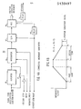
- Fig. 3 shows an example of a registration system utilizing this iterative technique.
- Fig. 3 illustrates in highly schematic form an E-beam column 10 having an E-beam source 12 emitting a scanning beam 14 through various deflection plates 16.
- the beam 14 is steered as shown in Fig. 3 onto a sample 18 positioned on an X-Y table 20 within the evacuated E-beam column.
- E-beam generation, deflection and scanning techniques are well known in the technology.
- backscattered electron sensors 22, 24 are positioned above the sample 18 to receive and sense backscattered electrons 26 emitted as a result of E-beam impingement onto the sample 18.
- a signal from sensors 22, 24 is supplied to a backscattered electron detector 28 which is used to provide an input to the correction increment generator 30.
- the correction increment generator 30 integrates the signal during each pair of scans and digitizes the resulting value.
- the correction increment generator 30 produces an output representing the difference of the value received by the correction increment generator for each of the scans. This output is a position correction increment.
- the value is used as an input to the correction generator 32 which adds the increment to the existing position correction value thereby generating an updated position correction value used as an input to the beam position correction driver 34.
- the beam position correction driver 34 converts the position correction value received from the correction generator 32 into an analog signal. This analog correction signal is supplied to the beam position driver 36 which is used to reposition the beam via a control input to steering plates 16.
- Fig. 4A a block diagram of the correction increment generator 30 in Fig. 3 is shown.
- the signal from the backscattered electron detector 28 provides input to the integrator 40, either directly or through the inverter 41.
- the inverter 41 is used during the first scan (T1 to T2) for example, and bypassed during the second scan (T3 to T4) by using switch 43 actuated by a lst/2nd scan control signal.
- Integrator 40 has its operation controlled by a Reset signal and an Integrate/Hold signal from the digital controller (not shown).
- the reset line is employed to zero the integrator.
- the integrate/hold line enables integration to occur when a feature edge is being scanned or causes the integrated signal to be held until after the sample and hold (S/H) module 42 is set to hold.
- the system controller uses the Convert Scan Value signal line to set the sample and hold module 42 to a hold mode.
- a signal is provided to the analog to digital converter 46 to convert the analog input level received from the sanple and hold module 42 into equivalent digital value. Wher the A/I sion it outputs the digitized Position Correction Increment, which is used as an input to a correction generator 32, and a Data Ready signal.
- a first input to the correction generator is the position correction increment signal.
- the correction generator accepts this position correction increment value as an input and adds it to the present correction value thereby generating an output which is the updated Position Correction Value sent to a beam position correction driver.
- the correction generator utilizes an adder 60 receiving the position correction increment signal as one input.
- a present correction generator 62 holds the present correction value which is used to form a second input to the adder.
- the adder then combines the present correction signal with the position correction increment to provide a new correction value which is used to update register 62.
- This updated output, the new position correction value is used as the output of the correction generator forming an input to the beam position correction driver.
- the position correction increment is also fed to a comparator 64 receiving as a second input a "Maximum Increment For No Rescan" signal 66.
- the two values are compared in the comparator 64. If the correction increment exceeds the predetermined allowed limit, a signal is returned to the digital controller. This signal from the comparator will then cause the registration scanning to be repeated.
- the position correction value output from the present correction register 62 is used to form parallel inputs to a pair of correction registers, i.e. an X correction register 68 and a Y correction register 70.
- the value is strobed into one or the other of the registers 68 and 70, depending on the state of the X/Y correction line input to selection logic 72.
- That logic network receives as a second signal a data ready signal supplied from the correction increment generator shown in Fig. 4A as an output from delay 74 as further processed from the correction generator shown in Fig. 5 in a subsequent delay module 76.
- the ultimate data ready signal into logic network 72 provides a second input to the pair of AND gates such that the position correction value is strobed into either of the correction registers 68 or 70 at the proper time.
- the values in the X-register 68 and the Y-register 70 are continuously inputted to a pair of digital/analog converters 78, 80.
- the output of those converters are analog X and Y correction signals sent to the beam position driver 36.
- the beam position driver 36 adjusts beam position in accordance with known techniques. When either correction driver is updated, a Correction Applied signal is sent to the digital controller as a function of the output of the OR gate in logic network 72 as processed through delay circuitry 82.
- a registration technique having the ability to handle out of range registration conditions while enabling a maximum of registration sensitivity. This is accomplished by utilizing smaller width scans since the capture range is independent of correction range. The system also eliminates the need for precise pre-alignment.
- the present invention eliminates registration correction errors which are caused by backscattered current variations since it utilizes successive correction increments.
- the correction generator 32 allows, by comparison control, the registration scan to be repeated thereby controlling the correction error for successive samples, for example those of significantly varying material tolerances. Such is an important specific advance in this technology. The technique when employed for such samples will now be discussed.
- the translation error of the pair of scanned windows with respect to the feature is therefore related to the signal (S) obtained by taking the difference between the integrated signals obtained while scanning the right and left scan areas 1A and 1B.
- the difference signal can then be defined as:
- the scan length L is fixed.
- the clear and opaque backscattered signal levels/unit area, S A and S B are constant so that their difference (S A - S B ) will also be constant.
- the difference signal is proportional to the beam to pattern alignment difference, so that the signal can be used to correct the beam to pattern alignment.
- Limiting the final correction increment is accomplished utilizing the comparator 64 shown in Fig. 5 that signals the digital controller when the position correction value exceeds the value in which the position error limit would be exceeded. The position is updated and the feature is rescanned until the correction increment is acceptable.
- an alignment system for registration of a scanning beam utilizing backscattered electrons in a mask inspection tool having improved characteristics.
- the system allows the use of minimum scan widths in a registration process to thereby significantly increase registration sensitivity.
Landscapes
- Physics & Mathematics (AREA)
- Condensed Matter Physics & Semiconductors (AREA)
- General Physics & Mathematics (AREA)
- Engineering & Computer Science (AREA)
- Computer Hardware Design (AREA)
- Microelectronics & Electronic Packaging (AREA)
- Power Engineering (AREA)
- Chemical & Material Sciences (AREA)
- Analytical Chemistry (AREA)
- Electron Beam Exposure (AREA)
- Length-Measuring Devices Using Wave Or Particle Radiation (AREA)
Applications Claiming Priority (2)
| Application Number | Priority Date | Filing Date | Title |
|---|---|---|---|
| US06/509,515 US4546260A (en) | 1983-06-30 | 1983-06-30 | Alignment technique |
| US509515 | 1983-06-30 |
Publications (3)
| Publication Number | Publication Date |
|---|---|
| EP0130497A2 true EP0130497A2 (fr) | 1985-01-09 |
| EP0130497A3 EP0130497A3 (en) | 1985-03-13 |
| EP0130497B1 EP0130497B1 (fr) | 1987-10-14 |
Family
ID=24026930
Family Applications (1)
| Application Number | Title | Priority Date | Filing Date |
|---|---|---|---|
| EP84107152A Expired EP0130497B1 (fr) | 1983-06-30 | 1984-06-22 | Technique d'alignement pour un faisceau de balayage |
Country Status (4)
| Country | Link |
|---|---|
| US (1) | US4546260A (fr) |
| EP (1) | EP0130497B1 (fr) |
| JP (1) | JPS6010725A (fr) |
| DE (1) | DE3466831D1 (fr) |
Cited By (2)
| Publication number | Priority date | Publication date | Assignee | Title |
|---|---|---|---|---|
| NL1005515C2 (nl) * | 1996-03-13 | 1998-07-20 | Analogic Corp | Gecomputeriseerde tomografiestelsels met bewegingsartefactonderdrukkingsfilter. |
| US6852988B2 (en) * | 2000-11-28 | 2005-02-08 | Sumitomo Heavy Industries, Ltd. | Gap adjustment apparatus and gap adjustment method for adjusting gap between two objects |
Families Citing this family (6)
| Publication number | Priority date | Publication date | Assignee | Title |
|---|---|---|---|---|
| FR2559695B1 (fr) * | 1984-02-20 | 1995-04-21 | Mitsubishi Electric Corp | Procede et appareil pour detecter et reguler la position d'un faisceau electronique de soudage |
| US5172117A (en) * | 1989-06-19 | 1992-12-15 | Linear Instruments | Analog to digital conversion using an integrater and a sample and hold circuit |
| JP2708300B2 (ja) * | 1991-10-21 | 1998-02-04 | 株式会社日立製作所 | 電子線描画方法 |
| US5345085A (en) * | 1993-03-26 | 1994-09-06 | Etec Systems, Inc. | Method and structure for electronically measuring beam parameters |
| US6107636A (en) * | 1997-02-07 | 2000-08-22 | Canon Kabushiki Kaisha | Electron beam exposure apparatus and its control method |
| US6146910A (en) * | 1999-02-02 | 2000-11-14 | The United States Of America, As Represented By The Secretary Of Commerce | Target configuration and method for extraction of overlay vectors from targets having concealed features |
Citations (5)
| Publication number | Priority date | Publication date | Assignee | Title |
|---|---|---|---|---|
| DE2117193A1 (de) * | 1971-04-08 | 1972-10-12 | Licentia Gmbh | Anordnung zur Feinpositionierung eines Elektronenstrahles |
| US3876883A (en) * | 1972-06-30 | 1975-04-08 | Ibm | Method and system for focusing and registration in electron beam projection microfabrication |
| EP0024884A2 (fr) * | 1979-08-29 | 1981-03-11 | Fujitsu Limited | Procédé pour détecter la position d'un substrat à l'aide d'un faisceau d'électrons |
| EP0027497A2 (fr) * | 1979-09-27 | 1981-04-29 | International Business Machines Corporation | Système de projection de rayons corpusculairs |
| EP0054710A1 (fr) * | 1980-12-19 | 1982-06-30 | International Business Machines Corporation | Procédé de positionnement et de contrôle d'une pièce munie de motifs, par exemple d'un masque pour la fabrication d'éléments semiconducteurs |
Family Cites Families (16)
| Publication number | Priority date | Publication date | Assignee | Title |
|---|---|---|---|---|
| US3519788A (en) * | 1967-01-13 | 1970-07-07 | Ibm | Automatic registration of an electron beam |
| US3575588A (en) * | 1968-09-09 | 1971-04-20 | Ibm | Electron beam circuit pattern generator for tracing microcircuit wire patterns on photoresist overlaid substrates |
| US3670153A (en) * | 1970-10-08 | 1972-06-13 | Rca Corp | Machine implemented method for positioning and inspecting an object |
| US3955072A (en) * | 1971-03-22 | 1976-05-04 | Kasper Instruments, Inc. | Apparatus for the automatic alignment of two superimposed objects for example a semiconductor wafer and a transparent mask |
| US3924113A (en) * | 1973-06-08 | 1975-12-02 | Ibm | Electron beam registration system |
| US4052603A (en) * | 1974-12-23 | 1977-10-04 | International Business Machines Corporation | Object positioning process and apparatus |
| JPS5212577A (en) * | 1975-07-21 | 1977-01-31 | Nippon Kogaku Kk <Nikon> | Automatic location device |
| US4209830A (en) * | 1976-04-19 | 1980-06-24 | Tokyo Shibaura Electric Co., Ltd. | Fine object having position and direction sensing mark and a system for detecting the position and direction of the sensing mark |
| US4203064A (en) * | 1977-04-05 | 1980-05-13 | Tokyo Shibaura Electric Co., Ltd. | Method for automatically controlling the position of small objects |
| JPS53148393A (en) * | 1977-05-31 | 1978-12-23 | Fujitsu Ltd | Positioning method |
| CH643959A5 (de) * | 1978-04-14 | 1984-06-29 | Siemens Ag | Verfahren und vorrichtung zur automatischen lageerkennung von halbleiterchips. |
| JPS54143070A (en) * | 1978-04-28 | 1979-11-07 | Nippon Telegr & Teleph Corp <Ntt> | Positioning unit of electron-beam exposure unit |
| JPS5546552A (en) * | 1978-09-28 | 1980-04-01 | Chiyou Lsi Gijutsu Kenkyu Kumiai | Method of positioning electron beam |
| DE2910580C3 (de) * | 1979-03-17 | 1982-01-21 | Texas Instruments Deutschland Gmbh, 8050 Freising | Ausrichtvorrichtung |
| US4365163A (en) * | 1980-12-19 | 1982-12-21 | International Business Machines Corporation | Pattern inspection tool - method and apparatus |
| US4357540A (en) * | 1980-12-19 | 1982-11-02 | International Business Machines Corporation | Semiconductor device array mask inspection method and apparatus |
-
1983
- 1983-06-30 US US06/509,515 patent/US4546260A/en not_active Expired - Fee Related
-
1984
- 1984-02-20 JP JP59028818A patent/JPS6010725A/ja active Pending
- 1984-06-22 DE DE8484107152T patent/DE3466831D1/de not_active Expired
- 1984-06-22 EP EP84107152A patent/EP0130497B1/fr not_active Expired
Patent Citations (5)
| Publication number | Priority date | Publication date | Assignee | Title |
|---|---|---|---|---|
| DE2117193A1 (de) * | 1971-04-08 | 1972-10-12 | Licentia Gmbh | Anordnung zur Feinpositionierung eines Elektronenstrahles |
| US3876883A (en) * | 1972-06-30 | 1975-04-08 | Ibm | Method and system for focusing and registration in electron beam projection microfabrication |
| EP0024884A2 (fr) * | 1979-08-29 | 1981-03-11 | Fujitsu Limited | Procédé pour détecter la position d'un substrat à l'aide d'un faisceau d'électrons |
| EP0027497A2 (fr) * | 1979-09-27 | 1981-04-29 | International Business Machines Corporation | Système de projection de rayons corpusculairs |
| EP0054710A1 (fr) * | 1980-12-19 | 1982-06-30 | International Business Machines Corporation | Procédé de positionnement et de contrôle d'une pièce munie de motifs, par exemple d'un masque pour la fabrication d'éléments semiconducteurs |
Non-Patent Citations (5)
| Title |
|---|
| IBM JOURNAL OF RESEARCH AND DEVELOPMENT, vol. 21, no. 6, November 1977, New York D.E. DAVIS et al.: "Automatic Registration in an Electron-Beam Lithographic System" pages 498-505 * |
| IBM JOURNAL OF RESEARCH AND DEVELOPMENT, vol. 21, no. 6, November 1977, New York H. ENGELKE et al.: "Correction of Nonlinear Deflection Distortion in a Direct Exposure Electron-Beam-System" pages 506-513 * |
| IBM JOURNAL OF RESEARCH AND DEVELOPMENT, vol. 24, no. 5, September 1980, New York D.E. DAVIS: "Registration Mark Detection for Electron-Beam Lithography-EL1 System" pages 545-553 * |
| IBM JOURNAL OF RESEARCH AND DEVELOPMENT, vol. 24, no. 5, September 1980, New York. D. E. DAVIS: "Registration Mark Detection for Electron-Beam Lithography-ELI System", pages 545-553 * |
| IBM JOURNAL OF RESEARCH AND DEVLOPMENT, vol. 21, no. 6, November 1977, New York. H. ENGELKE et al.: "Correction of Nonlinear Deflection Distortion in a Direct Exposure Electron-Beam-Sytem", pages 506-513 * |
Cited By (4)
| Publication number | Priority date | Publication date | Assignee | Title |
|---|---|---|---|---|
| NL1005515C2 (nl) * | 1996-03-13 | 1998-07-20 | Analogic Corp | Gecomputeriseerde tomografiestelsels met bewegingsartefactonderdrukkingsfilter. |
| US6852988B2 (en) * | 2000-11-28 | 2005-02-08 | Sumitomo Heavy Industries, Ltd. | Gap adjustment apparatus and gap adjustment method for adjusting gap between two objects |
| US7123997B2 (en) | 2000-11-28 | 2006-10-17 | Sumitomo Heavy Industries Ltd. | Gap adjustment apparatus and gap adjustment method for adjusting gap between two objects |
| US7225048B2 (en) | 2000-11-28 | 2007-05-29 | Sumitomo Heavy Industries, Ltd. | Gap adjustment apparatus and gap adjustment method for adjusting gap between two objects |
Also Published As
| Publication number | Publication date |
|---|---|
| EP0130497A3 (en) | 1985-03-13 |
| JPS6010725A (ja) | 1985-01-19 |
| US4546260A (en) | 1985-10-08 |
| DE3466831D1 (en) | 1987-11-19 |
| EP0130497B1 (fr) | 1987-10-14 |
Similar Documents
| Publication | Publication Date | Title |
|---|---|---|
| US4145597A (en) | Electron beam lithographic system | |
| US4423959A (en) | Positioning apparatus | |
| EP0024884B1 (fr) | Procédé pour détecter la position d'un substrat à l'aide d'un faisceau d'électrons | |
| US4119854A (en) | Electron beam exposure system | |
| US4701053A (en) | Mark position detecting method and apparatus | |
| EP0105185B1 (fr) | Méthode pour mesurer la position d'un corps de target d'un système d'exposition d'un modèle précis par un faisceau de particules chargées | |
| US4199688A (en) | Apparatus for electron beam lithography | |
| US4357540A (en) | Semiconductor device array mask inspection method and apparatus | |
| EP0130497A2 (fr) | Technique d'alignement pour un faisceau de balayage | |
| EP0083413A1 (fr) | Dispositif autofocus pour système lithographique par faisceau à électrons | |
| JPH0220921B2 (fr) | ||
| EP0023810B1 (fr) | Procédé d'exposition d'un faisceau électronique | |
| JPH0135493B2 (fr) | ||
| US4264822A (en) | Electron beam testing method and apparatus of mask | |
| EP0307906B1 (fr) | Compensation d'effets de courant parasite dans des systèmes de rayons de particules chargées | |
| JP2001085300A (ja) | マーク検出方法、電子線装置及び半導体デバイス製造方法 | |
| JPS62149127A (ja) | 荷電ビ−ム露光装置 | |
| JP2848417B2 (ja) | 荷電粒子ビーム露光装置および露光方法 | |
| JP2786662B2 (ja) | 荷電ビーム描画方法 | |
| JPH077742B2 (ja) | 電子ビーム露光方法 | |
| JP2828320B2 (ja) | 電子ビーム測長方法 | |
| JPH0328049B2 (fr) | ||
| JPS61120908A (ja) | マ−ク位置検出装置 | |
| JPH02142044A (ja) | 荷電粒子線装置 | |
| JPH0630332B2 (ja) | 位置決め装置、及び該装置を用いた基板の位置決め方法 |
Legal Events
| Date | Code | Title | Description |
|---|---|---|---|
| PUAI | Public reference made under article 153(3) epc to a published international application that has entered the european phase |
Free format text: ORIGINAL CODE: 0009012 |
|
| AK | Designated contracting states |
Designated state(s): DE FR GB |
|
| PUAL | Search report despatched |
Free format text: ORIGINAL CODE: 0009013 |
|
| 17P | Request for examination filed |
Effective date: 19841123 |
|
| AK | Designated contracting states |
Designated state(s): DE FR GB |
|
| 17Q | First examination report despatched |
Effective date: 19860722 |
|
| GRAA | (expected) grant |
Free format text: ORIGINAL CODE: 0009210 |
|
| AK | Designated contracting states |
Kind code of ref document: B1 Designated state(s): DE FR GB |
|
| REF | Corresponds to: |
Ref document number: 3466831 Country of ref document: DE Date of ref document: 19871119 |
|
| ET | Fr: translation filed | ||
| PLBE | No opposition filed within time limit |
Free format text: ORIGINAL CODE: 0009261 |
|
| STAA | Information on the status of an ep patent application or granted ep patent |
Free format text: STATUS: NO OPPOSITION FILED WITHIN TIME LIMIT |
|
| 26N | No opposition filed | ||
| PGFP | Annual fee paid to national office [announced via postgrant information from national office to epo] |
Ref country code: GB Payment date: 19920506 Year of fee payment: 9 |
|
| PGFP | Annual fee paid to national office [announced via postgrant information from national office to epo] |
Ref country code: FR Payment date: 19920601 Year of fee payment: 9 |
|
| PGFP | Annual fee paid to national office [announced via postgrant information from national office to epo] |
Ref country code: DE Payment date: 19920619 Year of fee payment: 9 |
|
| PG25 | Lapsed in a contracting state [announced via postgrant information from national office to epo] |
Ref country code: GB Effective date: 19930622 |
|
| GBPC | Gb: european patent ceased through non-payment of renewal fee |
Effective date: 19930622 |
|
| PG25 | Lapsed in a contracting state [announced via postgrant information from national office to epo] |
Ref country code: FR Effective date: 19940228 |
|
| PG25 | Lapsed in a contracting state [announced via postgrant information from national office to epo] |
Ref country code: DE Effective date: 19940301 |
|
| REG | Reference to a national code |
Ref country code: FR Ref legal event code: ST |