EP0130340B1 - System zur Abbildung und zum Auslesen eines Speichers - Google Patents
System zur Abbildung und zum Auslesen eines Speichers Download PDFInfo
- Publication number
- EP0130340B1 EP0130340B1 EP84105759A EP84105759A EP0130340B1 EP 0130340 B1 EP0130340 B1 EP 0130340B1 EP 84105759 A EP84105759 A EP 84105759A EP 84105759 A EP84105759 A EP 84105759A EP 0130340 B1 EP0130340 B1 EP 0130340B1
- Authority
- EP
- European Patent Office
- Prior art keywords
- bit
- address portion
- bits
- address
- data
- Prior art date
- Legal status (The legal status is an assumption and is not a legal conclusion. Google has not performed a legal analysis and makes no representation as to the accuracy of the status listed.)
- Expired
Links
Images


Classifications
-
- G—PHYSICS
- G06—COMPUTING; CALCULATING OR COUNTING
- G06F—ELECTRIC DIGITAL DATA PROCESSING
- G06F12/00—Accessing, addressing or allocating within memory systems or architectures
- G06F12/02—Addressing or allocation; Relocation
- G06F12/0207—Addressing or allocation; Relocation with multidimensional access, e.g. row/column, matrix
-
- G—PHYSICS
- G11—INFORMATION STORAGE
- G11C—STATIC STORES
- G11C8/00—Arrangements for selecting an address in a digital store
Landscapes
- Engineering & Computer Science (AREA)
- Physics & Mathematics (AREA)
- Theoretical Computer Science (AREA)
- Microelectronics & Electronic Packaging (AREA)
- Mathematical Physics (AREA)
- General Engineering & Computer Science (AREA)
- General Physics & Mathematics (AREA)
- Image Input (AREA)
- Memory System (AREA)
Claims (2)
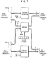
dadurch gekennzeichnet, daß die Datenwort-Adressen einen Adressenabschnitt für hohe Wörter und einen Adressenabschnitt für niedrige Wörter (WL) enthalten, und Datenbitadressen einen Adressenabschnitt für hohe Bits (BH) und einen Adressenabschnitt für niedrige Bits enthalten und besagter Niedrigbit-Adressenabschnitt und besagte Speichermittel Adressengeneratormittel (Abb. 3) enthalten, für die Verschiebung von Adressen mit einer horizontalen und einer vertikalen Betriebsart und mindestens ein Inkrementierglied, das besagten Hochwortadressenabschnitt und besagten Niedrigbitadressenabschnitt inkrementiert, Chipzahlspeichermittel für die Bereitstellung von Chipzahlbits und ein Addierelement, in dem besagter Niedrigwortadressenabschnitt (WL) und besagter Hochbitadressenabschnitt (BH) am Eingang des Addierelements verkettet sind, und in der vertikalen Betriebsart die Chip-Zahl zu den verketteten Bits addiert wird und der Addierglied-Ausgang mit dem Ausgang des besagten Inkrementierglieds verbunden ist, um eine verschobene Datenwortadresse und eine verschobene Datenbitadresse zu erzeugen, wodurch der Addiergliedausgang geteilt wird, auf der einen Seite in hohe Bits, die dem besagten Niedrigwortadressenabschnitt (WL) entsprechen, und auf der anderen Seite, in Niedrigbits, die dem besagten Hochbitadressenabschnitt (BH) entsprechen, und besagte Hochbits mit besagtem Hochwortadressenabschnitt verkettet sind und besagte Niedrigbitsmit besagtem Niedrigbitadressenabschnitt verkettet sind.
Applications Claiming Priority (2)
| Application Number | Priority Date | Filing Date | Title |
|---|---|---|---|
| US06/509,697 US4559611A (en) | 1983-06-30 | 1983-06-30 | Mapping and memory hardware for writing horizontal and vertical lines |
| US509697 | 1983-06-30 |
Publications (3)
| Publication Number | Publication Date |
|---|---|
| EP0130340A2 EP0130340A2 (de) | 1985-01-09 |
| EP0130340A3 EP0130340A3 (en) | 1987-11-25 |
| EP0130340B1 true EP0130340B1 (de) | 1990-09-12 |
Family
ID=24027734
Family Applications (1)
| Application Number | Title | Priority Date | Filing Date |
|---|---|---|---|
| EP84105759A Expired EP0130340B1 (de) | 1983-06-30 | 1984-05-21 | System zur Abbildung und zum Auslesen eines Speichers |
Country Status (4)
| Country | Link |
|---|---|
| US (1) | US4559611A (de) |
| EP (1) | EP0130340B1 (de) |
| JP (1) | JPS6015688A (de) |
| DE (1) | DE3483181D1 (de) |
Families Citing this family (6)
| Publication number | Priority date | Publication date | Assignee | Title |
|---|---|---|---|---|
| FR2566950B1 (fr) * | 1984-06-29 | 1986-12-26 | Texas Instruments France | Processeur de points d'images video, systeme de visualisation en comportant application et procede pour sa mise en oeuvre |
| US4912658A (en) * | 1986-04-18 | 1990-03-27 | Advanced Micro Devices, Inc. | Method and apparatus for addressing video RAMS and refreshing a video monitor with a variable resolution |
| US4716546A (en) * | 1986-07-30 | 1987-12-29 | International Business Machines Corporation | Memory organization for vertical and horizontal vectors in a raster scan display system |
| JPS63177235A (ja) * | 1987-01-19 | 1988-07-21 | Fujitsu Ltd | 多次元アクセスメモリ |
| GB2250615B (en) * | 1990-11-21 | 1995-06-14 | Apple Computer | Apparatus for performing direct memory access with stride |
| US5235613A (en) * | 1992-03-02 | 1993-08-10 | The Boeing Company | Frequency hopping method and apparatus |
Family Cites Families (18)
| Publication number | Priority date | Publication date | Assignee | Title |
|---|---|---|---|---|
| US3292151A (en) * | 1962-06-04 | 1966-12-13 | Ibm | Memory expansion |
| FR1543788A (fr) * | 1966-12-28 | Ibm | Système de mémoire à accès sélectif multidirectionnel à mots multiples | |
| US3588829A (en) * | 1968-11-14 | 1971-06-28 | Ibm | Integrated memory system with block transfer to a buffer store |
| US3737866A (en) * | 1971-07-27 | 1973-06-05 | Data General Corp | Data storage and retrieval system |
| US4020470A (en) * | 1975-06-06 | 1977-04-26 | Ibm Corporation | Simultaneous addressing of different locations in a storage unit |
| US4024508A (en) * | 1975-06-19 | 1977-05-17 | Honeywell Information Systems, Inc. | Database instruction find serial |
| US4025901A (en) * | 1975-06-19 | 1977-05-24 | Honeywell Information Systems, Inc. | Database instruction find owner |
| US4090174A (en) * | 1976-11-01 | 1978-05-16 | International Business Machines Corporation | Method and apparatus for accessing horizontal sequences, vertical sequences and rectangular subarrays from an array stored in a modified word organized random access memory system |
| US4126897A (en) * | 1977-07-05 | 1978-11-21 | International Business Machines Corporation | Request forwarding system |
| US4128873A (en) * | 1977-09-20 | 1978-12-05 | Burroughs Corporation | Structure for an easily testable single chip calculator/controller |
| US4195342A (en) * | 1977-12-22 | 1980-03-25 | Honeywell Information Systems Inc. | Multi-configurable cache store system |
| US4296467A (en) * | 1978-07-03 | 1981-10-20 | Honeywell Information Systems Inc. | Rotating chip selection technique and apparatus |
| US4309755A (en) * | 1979-08-22 | 1982-01-05 | Bell Telephone Laboratories, Incorporated | Computer input/output arrangement for enabling a simultaneous read/write data transfer |
| JPS56118145A (en) * | 1980-02-22 | 1981-09-17 | Ricoh Co Ltd | Processor for video information |
| DE3015125A1 (de) * | 1980-04-19 | 1981-10-22 | Ibm Deutschland Gmbh, 7000 Stuttgart | Einrichtung zur speicherung und darstellung graphischer information |
| US4370732A (en) * | 1980-09-15 | 1983-01-25 | Ibm Corporation | Skewed matrix address generator |
| JPS5784486A (en) * | 1980-11-13 | 1982-05-26 | Usac Denshi Kogyo Kk | Character generator |
| US4402043A (en) * | 1980-11-24 | 1983-08-30 | Texas Instruments Incorporated | Microprocessor with compressed control ROM |
-
1983
- 1983-06-30 US US06/509,697 patent/US4559611A/en not_active Expired - Lifetime
-
1984
- 1984-03-19 JP JP59051295A patent/JPS6015688A/ja active Pending
- 1984-05-21 DE DE8484105759T patent/DE3483181D1/de not_active Expired - Fee Related
- 1984-05-21 EP EP84105759A patent/EP0130340B1/de not_active Expired
Also Published As
| Publication number | Publication date |
|---|---|
| US4559611A (en) | 1985-12-17 |
| EP0130340A3 (en) | 1987-11-25 |
| EP0130340A2 (de) | 1985-01-09 |
| DE3483181D1 (de) | 1990-10-18 |
| JPS6015688A (ja) | 1985-01-26 |
Similar Documents
| Publication | Publication Date | Title |
|---|---|---|
| EP0225059B1 (de) | Halbleiterspeicher | |
| EP0492939B1 (de) | Verfahren und Einrichtung zur Zugriffsanordnung eines VRAM zum beschleunigten Schreiben von vertikalen Linien auf einer Anzeige | |
| US5321510A (en) | Serial video processor | |
| US4561072A (en) | Memory system handling a plurality of bits as a unit to be processed | |
| CA2027458A1 (en) | Method to rotate a bit map image 90 degrees | |
| JP3278756B2 (ja) | 画像処理方法及び装置 | |
| EP0744712A2 (de) | Speicherschaltung für Texturmuster | |
| KR910002202B1 (ko) | 바운더리-프리 반도체 메모리 장치 | |
| US5361339A (en) | Circuit for fast page mode addressing of a RAM with multiplexed row and column address lines | |
| EP0130340B1 (de) | System zur Abbildung und zum Auslesen eines Speichers | |
| US5230064A (en) | High resolution graphic display organization | |
| GB2174277A (en) | Method and system for displaying multiple images on a display screen | |
| US5412740A (en) | Signal processing system having reduced memory space | |
| US6085304A (en) | Interface for processing element array | |
| EP0367995B1 (de) | Vektordatenübertragungssteuerung | |
| US5008852A (en) | Parallel accessible memory device | |
| JPH06167958A (ja) | 記憶装置 | |
| US6680736B1 (en) | Graphic display systems having paired memory arrays therein that can be row accessed with 2(2n) degrees of freedom | |
| US4888584A (en) | Vector pattern processing circuit for bit map display system | |
| Ericsson et al. | LIPP-A SIMD multiprocessor architecture for image processing | |
| EP0549309A1 (de) | Adressverminderungsschema zur Durchführung eines Rotationsalgorithmus | |
| JPH028335B2 (de) | ||
| JP2633251B2 (ja) | 画像メモリ素子 | |
| JPH03196376A (ja) | 全フイールド記憶装置から複数の隣接記憶位置に並列にアクセスするアドレス指定機構 | |
| JPS62151987A (ja) | 画像処理用マルチ・ポ−ト・メモリ |
Legal Events
| Date | Code | Title | Description |
|---|---|---|---|
| PUAI | Public reference made under article 153(3) epc to a published international application that has entered the european phase |
Free format text: ORIGINAL CODE: 0009012 |
|
| AK | Designated contracting states |
Designated state(s): DE FR GB |
|
| 17P | Request for examination filed |
Effective date: 19841123 |
|
| PUAL | Search report despatched |
Free format text: ORIGINAL CODE: 0009013 |
|
| AK | Designated contracting states |
Kind code of ref document: A3 Designated state(s): DE FR GB |
|
| 17Q | First examination report despatched |
Effective date: 19880511 |
|
| GRAA | (expected) grant |
Free format text: ORIGINAL CODE: 0009210 |
|
| AK | Designated contracting states |
Kind code of ref document: B1 Designated state(s): DE FR GB |
|
| REF | Corresponds to: |
Ref document number: 3483181 Country of ref document: DE Date of ref document: 19901018 |
|
| ET | Fr: translation filed | ||
| PLBE | No opposition filed within time limit |
Free format text: ORIGINAL CODE: 0009261 |
|
| STAA | Information on the status of an ep patent application or granted ep patent |
Free format text: STATUS: NO OPPOSITION FILED WITHIN TIME LIMIT |
|
| 26N | No opposition filed | ||
| PGFP | Annual fee paid to national office [announced via postgrant information from national office to epo] |
Ref country code: GB Payment date: 19940415 Year of fee payment: 11 |
|
| PGFP | Annual fee paid to national office [announced via postgrant information from national office to epo] |
Ref country code: FR Payment date: 19940427 Year of fee payment: 11 |
|
| PGFP | Annual fee paid to national office [announced via postgrant information from national office to epo] |
Ref country code: DE Payment date: 19940513 Year of fee payment: 11 |
|
| PG25 | Lapsed in a contracting state [announced via postgrant information from national office to epo] |
Ref country code: GB Effective date: 19950521 |
|
| GBPC | Gb: european patent ceased through non-payment of renewal fee |
Effective date: 19950521 |
|
| PG25 | Lapsed in a contracting state [announced via postgrant information from national office to epo] |
Ref country code: DE Effective date: 19960201 |
|
| PG25 | Lapsed in a contracting state [announced via postgrant information from national office to epo] |
Ref country code: FR Effective date: 19960229 |
|
| REG | Reference to a national code |
Ref country code: FR Ref legal event code: ST |
|
| REG | Reference to a national code |
Ref country code: FR Ref legal event code: ST |