EP0130340A2 - System zur Abbildung und zum Auslesen eines Speichers - Google Patents
System zur Abbildung und zum Auslesen eines Speichers Download PDFInfo
- Publication number
- EP0130340A2 EP0130340A2 EP84105759A EP84105759A EP0130340A2 EP 0130340 A2 EP0130340 A2 EP 0130340A2 EP 84105759 A EP84105759 A EP 84105759A EP 84105759 A EP84105759 A EP 84105759A EP 0130340 A2 EP0130340 A2 EP 0130340A2
- Authority
- EP
- European Patent Office
- Prior art keywords
- address
- bits
- data
- bit
- word
- Prior art date
- Legal status (The legal status is an assumption and is not a legal conclusion. Google has not performed a legal analysis and makes no representation as to the accuracy of the status listed.)
- Granted
Links
Images


Classifications
-
- G—PHYSICS
- G06—COMPUTING; CALCULATING OR COUNTING
- G06F—ELECTRIC DIGITAL DATA PROCESSING
- G06F12/00—Accessing, addressing or allocating within memory systems or architectures
- G06F12/02—Addressing or allocation; Relocation
- G06F12/0207—Addressing or allocation; Relocation with multidimensional access, e.g. row/column, matrix
-
- G—PHYSICS
- G11—INFORMATION STORAGE
- G11C—STATIC STORES
- G11C8/00—Arrangements for selecting an address in a digital store
Definitions
- the present invention relates to digital data processing memories, and more particularly to a memory mapping and readout system for storing a two-dimensional array of data bits on a collection of memory chips, to allow horizontal or vertical bit readout of the array.
- U.S. Patent 3,466,611 issued Sept. 9, 1969 to A. Weinberger, entitled “Multi-Word Multi-Directional Random Access Memory System” discloses a computer memory configuration wherein multi-word access within the memory is possible in a plurality of directions.
- U.S. Patent 4,296,467 issued Oct. 20, 1981 to Nibby, Jr. et al describes a rotating chip selection technique in memory subsystem which includes at least one up to a number of memory module boards identical in layout and construction.
- the board includes a number of memory chips which are positioned at an initial physical row location providing a predetermined number of addressable contiguous memory locations corresponding to a predetermined increment of memory capacity.
- the board further includes a register for receiving address signals for accessing the contents of a memory location, rotating chip selection circuits which include a set of switches and an arithmetic unit having first and second sets of input terminals.
- the first set of input terminals is connected to the register for receiving predetermined ones of the address signals representative of the physical row location of chips being addressed and the second set of input terminals are connected to receive signals from the set of switches.
- the arithmetic unit operates to perform a predetermined arithmetic operation upon the signals applied to the sets of input terminals to generate a set of logical row address signals for enabling the number of chips at the initial row location. None of the references shows the mapping technique and hardware of the present invention.
- An object of the present invention is to provide structures for writing horizontal and vertical bit strings into a two-dimensional computer memory which is composed of a collection of memory chips.
- Another object of the present invention is to provide memory structure to provide bit addressability in both horizontal and vertical directions. Still another object of the present invention is to provide a display system for mapping from a frame buffer to a high function raster-scan display screen with the enhanced structure for writing vertical bit strings at the same speed as horizontal bit strings.
- mappings for storing an array in 64K memory chips, and the required data transformations, address calculations, and chip hardware.
- the mapping and hardware provide bit addressability in both horizontal and vertical directions.
- removal of the incrementer associated with the word and/or bit address will remove the bit addressability in the vertical and/or horizontal direction respectively, while still retaining the ability to write 16 bits beginning at even byte boundaries.
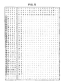
- FIG. 1 a two-dimensional array of data bits is illustrated and FIG. 2 shows the mapping of the array into the memory chips. It is seen that 16 horizontal bits are placed into corresponding locations in each chip with a bit increment for those chips associated with bits crossing an even byte boundary.
- the mapping of 16 vertical bits is somewhat more complicated, in that the bits are placed in corresponding locations in quadrants of different words. The quadrants increase by 1 modulo 4 and the words increase by 1 each time the quadrant becomes 0.
- This sequencing through quadrants and words is best described by associating a 4 bit quantity with location where the 2 low order bits define the quadrant and the 2 high order bits define the 2 low order bits of the word address. Sequencing through the locations then corresponds to sequencing through the consecutive numbers 0 to 15. For those bits that cross an even byte boundary, the word address must be increased by four.
- the important observation to be made about the mapping is that 16 horizontal or vertical bits can be written into memory in one cycle because no two bits are mapped to the same chip.
- X,Y is the screen address
- mode and bit and word addresses are broadcast to all chips; and each chip receives the appropriate data, mask and increment signal:
- the "16 take” can be deleted if it is assumed that 16 bits of data are always received.
- the term “16 take” indicates that the user may want to write less than 16 bits.
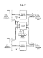
- FIG. 3 shows the on-chip hardware required for address translation.
- the translation affects only the two low order bits of the word address and the two high order bits of the bit address.
- the function performed is an addition of the 4 bit chip number from the chip number storage to the four bits formed by catenating BH and WL where BH is the two low order bits and WL is the two high order bits which are applied as inputs to the adder.
- the four bit result of the addition (ignoring carry out) is also the catenation of BH and WL in the same order as in the input.
- the six higher order bits of the word address and the six lower order bits of the bit address are applied to respective incrementer circuits as illustrated.
- the portion of the word and bit address that may be altered by their respective incrementers are disjoint from the portion that is modified by the 4 bit adder. Therefore, the incrementers can be removed independently from the remainder of the address translation hardware. Thus, a modified scheme can be implemented in which writing starts only on even byte boundaries in either or both horizontal and vertical directions. Further, it should be noted that the incrementer can be shared since at most, one of them is active during a given write operation.
- the adder and the incrementer circuits used in the structure of FIG. 3 are conventional state-of-the-art devices.
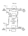
- FIG. 4 shows the scheme necessary for serializing the output bit stream.
- the only modification to the typical raster generation scheme of the prior art is the addition of hardware that increments the serializer position once after each scan line in order to account for the staggered storage pattern.
- Each READ into the output buffer provides enough data for four scan lines. These bits are scanned successively in the bit direction with the origin within the 16 buffers being incremented modulo 16 after every scan line.
- the screen signals are obtained from row buffer storage devices (i.e., 256 bit row buffer in the specific example of FIG. 4).
- the 16 chip row buffers will contain the first four scan lines of the 1K x 1K display.
- the scan lines are stored in a manner that provides easy access as indicated by the bit coordinates shown in FIG. 4.
- the multiplexing of addresses may be employed.
- the horizontal word address may be followed by a series of bit addresses.
- the same technique can be utilized, with the further novel aspect that in addition to the word address being followed by a series of bit addresses for the horizontal case, the bit address can be applied followed by a series of word addresses in the vertical case.
- the structure of FIGS. 3, 7, 9 and 10 is modified in that only one incrementer means is used with both the "word inc” signal and the "bit inc” signal being applied to the one incrementer in a time shared manner.
- the "word inc” signal is applied first.
- the "bit inc” signal is applied first.
- the invention was described as including a plurality of separate memory chips.
- each of the discrete memory locations required may, along with their associated circuits, be fabricated onto a single master chip.
Applications Claiming Priority (2)
| Application Number | Priority Date | Filing Date | Title |
|---|---|---|---|
| US06/509,697 US4559611A (en) | 1983-06-30 | 1983-06-30 | Mapping and memory hardware for writing horizontal and vertical lines |
| US509697 | 1983-06-30 |
Publications (3)
| Publication Number | Publication Date |
|---|---|
| EP0130340A2 true EP0130340A2 (de) | 1985-01-09 |
| EP0130340A3 EP0130340A3 (en) | 1987-11-25 |
| EP0130340B1 EP0130340B1 (de) | 1990-09-12 |
Family
ID=24027734
Family Applications (1)
| Application Number | Title | Priority Date | Filing Date |
|---|---|---|---|
| EP84105759A Expired EP0130340B1 (de) | 1983-06-30 | 1984-05-21 | System zur Abbildung und zum Auslesen eines Speichers |
Country Status (4)
| Country | Link |
|---|---|
| US (1) | US4559611A (de) |
| EP (1) | EP0130340B1 (de) |
| JP (1) | JPS6015688A (de) |
| DE (1) | DE3483181D1 (de) |
Cited By (2)
| Publication number | Priority date | Publication date | Assignee | Title |
|---|---|---|---|---|
| EP0244112A2 (de) * | 1986-04-18 | 1987-11-04 | Advanced Micro Devices, Inc. | Verfahren und Einrichtung zur Adressierung von Videorams und zum Auffrischen eines Videomonitors mit variablem Auflösungsvermögen |
| EP0276110A2 (de) * | 1987-01-19 | 1988-07-27 | Fujitsu Limited | Halbleiterspeicheranordnung |
Families Citing this family (4)
| Publication number | Priority date | Publication date | Assignee | Title |
|---|---|---|---|---|
| FR2566950B1 (fr) * | 1984-06-29 | 1986-12-26 | Texas Instruments France | Processeur de points d'images video, systeme de visualisation en comportant application et procede pour sa mise en oeuvre |
| US4716546A (en) * | 1986-07-30 | 1987-12-29 | International Business Machines Corporation | Memory organization for vertical and horizontal vectors in a raster scan display system |
| GB2250615B (en) * | 1990-11-21 | 1995-06-14 | Apple Computer | Apparatus for performing direct memory access with stride |
| US5235613A (en) * | 1992-03-02 | 1993-08-10 | The Boeing Company | Frequency hopping method and apparatus |
Citations (3)
| Publication number | Priority date | Publication date | Assignee | Title |
|---|---|---|---|---|
| US4090174A (en) * | 1976-11-01 | 1978-05-16 | International Business Machines Corporation | Method and apparatus for accessing horizontal sequences, vertical sequences and rectangular subarrays from an array stored in a modified word organized random access memory system |
| EP0038411A2 (de) * | 1980-04-19 | 1981-10-28 | International Business Machines Corporation | Einrichtung zur Speicherung und Darstellung graphischer Information |
| EP0047842A2 (de) * | 1980-09-15 | 1982-03-24 | International Business Machines Corporation | Adressengenerator für eine versetzte Matrix |
Family Cites Families (15)
| Publication number | Priority date | Publication date | Assignee | Title |
|---|---|---|---|---|
| US3292151A (en) * | 1962-06-04 | 1966-12-13 | Ibm | Memory expansion |
| FR1543788A (fr) * | 1966-12-28 | Ibm | Système de mémoire à accès sélectif multidirectionnel à mots multiples | |
| US3588829A (en) * | 1968-11-14 | 1971-06-28 | Ibm | Integrated memory system with block transfer to a buffer store |
| US3737866A (en) * | 1971-07-27 | 1973-06-05 | Data General Corp | Data storage and retrieval system |
| US4020470A (en) * | 1975-06-06 | 1977-04-26 | Ibm Corporation | Simultaneous addressing of different locations in a storage unit |
| US4024508A (en) * | 1975-06-19 | 1977-05-17 | Honeywell Information Systems, Inc. | Database instruction find serial |
| US4025901A (en) * | 1975-06-19 | 1977-05-24 | Honeywell Information Systems, Inc. | Database instruction find owner |
| US4126897A (en) * | 1977-07-05 | 1978-11-21 | International Business Machines Corporation | Request forwarding system |
| US4128873A (en) * | 1977-09-20 | 1978-12-05 | Burroughs Corporation | Structure for an easily testable single chip calculator/controller |
| US4195342A (en) * | 1977-12-22 | 1980-03-25 | Honeywell Information Systems Inc. | Multi-configurable cache store system |
| US4296467A (en) * | 1978-07-03 | 1981-10-20 | Honeywell Information Systems Inc. | Rotating chip selection technique and apparatus |
| US4309755A (en) * | 1979-08-22 | 1982-01-05 | Bell Telephone Laboratories, Incorporated | Computer input/output arrangement for enabling a simultaneous read/write data transfer |
| JPS56118145A (en) * | 1980-02-22 | 1981-09-17 | Ricoh Co Ltd | Processor for video information |
| JPS5784486A (en) * | 1980-11-13 | 1982-05-26 | Usac Denshi Kogyo Kk | Character generator |
| US4402043A (en) * | 1980-11-24 | 1983-08-30 | Texas Instruments Incorporated | Microprocessor with compressed control ROM |
-
1983
- 1983-06-30 US US06/509,697 patent/US4559611A/en not_active Expired - Lifetime
-
1984
- 1984-03-19 JP JP59051295A patent/JPS6015688A/ja active Pending
- 1984-05-21 DE DE8484105759T patent/DE3483181D1/de not_active Expired - Fee Related
- 1984-05-21 EP EP84105759A patent/EP0130340B1/de not_active Expired
Patent Citations (3)
| Publication number | Priority date | Publication date | Assignee | Title |
|---|---|---|---|---|
| US4090174A (en) * | 1976-11-01 | 1978-05-16 | International Business Machines Corporation | Method and apparatus for accessing horizontal sequences, vertical sequences and rectangular subarrays from an array stored in a modified word organized random access memory system |
| EP0038411A2 (de) * | 1980-04-19 | 1981-10-28 | International Business Machines Corporation | Einrichtung zur Speicherung und Darstellung graphischer Information |
| EP0047842A2 (de) * | 1980-09-15 | 1982-03-24 | International Business Machines Corporation | Adressengenerator für eine versetzte Matrix |
Cited By (4)
| Publication number | Priority date | Publication date | Assignee | Title |
|---|---|---|---|---|
| EP0244112A2 (de) * | 1986-04-18 | 1987-11-04 | Advanced Micro Devices, Inc. | Verfahren und Einrichtung zur Adressierung von Videorams und zum Auffrischen eines Videomonitors mit variablem Auflösungsvermögen |
| EP0244112A3 (de) * | 1986-04-18 | 1990-08-22 | Advanced Micro Devices, Inc. | Verfahren und Einrichtung zur Adressierung von Videorams und zum Auffrischen eines Videomonitors mit variablem Auflösungsvermögen |
| EP0276110A2 (de) * | 1987-01-19 | 1988-07-27 | Fujitsu Limited | Halbleiterspeicheranordnung |
| EP0276110A3 (de) * | 1987-01-19 | 1991-08-21 | Fujitsu Limited | Halbleiterspeicheranordnung |
Also Published As
| Publication number | Publication date |
|---|---|
| EP0130340B1 (de) | 1990-09-12 |
| US4559611A (en) | 1985-12-17 |
| EP0130340A3 (en) | 1987-11-25 |
| DE3483181D1 (de) | 1990-10-18 |
| JPS6015688A (ja) | 1985-01-26 |
Similar Documents
| Publication | Publication Date | Title |
|---|---|---|
| US5924111A (en) | Method and system for interleaving data in multiple memory bank partitions | |
| US5321510A (en) | Serial video processor | |
| EP0047842B1 (de) | Adressengenerator für eine versetzte Matrix | |
| EP0225059A2 (de) | Halbleiterspeicher | |
| US4561072A (en) | Memory system handling a plurality of bits as a unit to be processed | |
| EP0279228B1 (de) | Bildspeicher für Raster-Video-Anzeige | |
| KR910002202B1 (ko) | 바운더리-프리 반도체 메모리 장치 | |
| US4805173A (en) | Error control method and apparatus | |
| US5230064A (en) | High resolution graphic display organization | |
| US4559611A (en) | Mapping and memory hardware for writing horizontal and vertical lines | |
| US5361339A (en) | Circuit for fast page mode addressing of a RAM with multiplexed row and column address lines | |
| EP0317218B1 (de) | Serieller Videoprozessor und Verfahren | |
| GB2174277A (en) | Method and system for displaying multiple images on a display screen | |
| US6085304A (en) | Interface for processing element array | |
| CA2000145C (en) | Data transfer controller | |
| JPH05282437A (ja) | 画像回転回路 | |
| EP0342022A3 (de) | System zum Lesen von Bilddaten in einem digitalen Bildverarbeitungssystem | |
| GB2151440A (en) | A circuit for increasing the number of pixels in a scan of a bit mapping type video display | |
| JPH06167958A (ja) | 記憶装置 | |
| US6680736B1 (en) | Graphic display systems having paired memory arrays therein that can be row accessed with 2(2n) degrees of freedom | |
| US4888584A (en) | Vector pattern processing circuit for bit map display system | |
| JP2855899B2 (ja) | 機能メモリ | |
| JPS62151987A (ja) | 画像処理用マルチ・ポ−ト・メモリ | |
| JP2633251B2 (ja) | 画像メモリ素子 | |
| JPH07271966A (ja) | データ記憶方法並びにこれを用いたスクロール方法及びデータ出力方法 |
Legal Events
| Date | Code | Title | Description |
|---|---|---|---|
| PUAI | Public reference made under article 153(3) epc to a published international application that has entered the european phase |
Free format text: ORIGINAL CODE: 0009012 |
|
| AK | Designated contracting states |
Designated state(s): DE FR GB |
|
| 17P | Request for examination filed |
Effective date: 19841123 |
|
| PUAL | Search report despatched |
Free format text: ORIGINAL CODE: 0009013 |
|
| AK | Designated contracting states |
Kind code of ref document: A3 Designated state(s): DE FR GB |
|
| 17Q | First examination report despatched |
Effective date: 19880511 |
|
| GRAA | (expected) grant |
Free format text: ORIGINAL CODE: 0009210 |
|
| AK | Designated contracting states |
Kind code of ref document: B1 Designated state(s): DE FR GB |
|
| REF | Corresponds to: |
Ref document number: 3483181 Country of ref document: DE Date of ref document: 19901018 |
|
| ET | Fr: translation filed | ||
| PLBE | No opposition filed within time limit |
Free format text: ORIGINAL CODE: 0009261 |
|
| STAA | Information on the status of an ep patent application or granted ep patent |
Free format text: STATUS: NO OPPOSITION FILED WITHIN TIME LIMIT |
|
| 26N | No opposition filed | ||
| PGFP | Annual fee paid to national office [announced via postgrant information from national office to epo] |
Ref country code: GB Payment date: 19940415 Year of fee payment: 11 |
|
| PGFP | Annual fee paid to national office [announced via postgrant information from national office to epo] |
Ref country code: FR Payment date: 19940427 Year of fee payment: 11 |
|
| PGFP | Annual fee paid to national office [announced via postgrant information from national office to epo] |
Ref country code: DE Payment date: 19940513 Year of fee payment: 11 |
|
| PG25 | Lapsed in a contracting state [announced via postgrant information from national office to epo] |
Ref country code: GB Effective date: 19950521 |
|
| GBPC | Gb: european patent ceased through non-payment of renewal fee |
Effective date: 19950521 |
|
| PG25 | Lapsed in a contracting state [announced via postgrant information from national office to epo] |
Ref country code: DE Effective date: 19960201 |
|
| PG25 | Lapsed in a contracting state [announced via postgrant information from national office to epo] |
Ref country code: FR Effective date: 19960229 |
|
| REG | Reference to a national code |
Ref country code: FR Ref legal event code: ST |
|
| REG | Reference to a national code |
Ref country code: FR Ref legal event code: ST |