EP0125733A1 - Circuit utilisant des transistors à effet de champ complémentaires à perte isolée - Google Patents
Circuit utilisant des transistors à effet de champ complémentaires à perte isolée Download PDFInfo
- Publication number
- EP0125733A1 EP0125733A1 EP84200673A EP84200673A EP0125733A1 EP 0125733 A1 EP0125733 A1 EP 0125733A1 EP 84200673 A EP84200673 A EP 84200673A EP 84200673 A EP84200673 A EP 84200673A EP 0125733 A1 EP0125733 A1 EP 0125733A1
- Authority
- EP
- European Patent Office
- Prior art keywords
- transistor
- circuit
- voltage
- output
- gate
- Prior art date
- Legal status (The legal status is an assumption and is not a legal conclusion. Google has not performed a legal analysis and makes no representation as to the accuracy of the status listed.)
- Withdrawn
Links
Images

Classifications
-
- H—ELECTRICITY
- H03—ELECTRONIC CIRCUITRY
- H03K—PULSE TECHNIQUE
- H03K19/00—Logic circuits, i.e. having at least two inputs acting on one output; Inverting circuits
- H03K19/0175—Coupling arrangements; Interface arrangements
- H03K19/0185—Coupling arrangements; Interface arrangements using field effect transistors only
- H03K19/018507—Interface arrangements
- H03K19/018521—Interface arrangements of complementary type, e.g. CMOS
-
- H—ELECTRICITY
- H03—ELECTRONIC CIRCUITRY
- H03K—PULSE TECHNIQUE
- H03K19/00—Logic circuits, i.e. having at least two inputs acting on one output; Inverting circuits
- H03K19/02—Logic circuits, i.e. having at least two inputs acting on one output; Inverting circuits using specified components
- H03K19/08—Logic circuits, i.e. having at least two inputs acting on one output; Inverting circuits using specified components using semiconductor devices
- H03K19/094—Logic circuits, i.e. having at least two inputs acting on one output; Inverting circuits using specified components using semiconductor devices using field-effect transistors
- H03K19/0944—Logic circuits, i.e. having at least two inputs acting on one output; Inverting circuits using specified components using semiconductor devices using field-effect transistors using MOSFET or insulated gate field-effect transistors, i.e. IGFET
- H03K19/0948—Logic circuits, i.e. having at least two inputs acting on one output; Inverting circuits using specified components using semiconductor devices using field-effect transistors using MOSFET or insulated gate field-effect transistors, i.e. IGFET using CMOS or complementary insulated gate field-effect transistors
Definitions
- the invention relates to a voltage level adaptive circuit arrangement comprising an inverting logic gate circuit of complementary insulated gate field effect transistors, which transistors are arranged between a first and a second supply voltage tapping point, which gate has an output and at least one input.
- Inverting logic gate circuits of complementary field effect transistors are known per se (see, for example, the book “MOS/LSI-Design and Application", pages 113-115, published in 1972 by McGraw-Hill Book Company) and are frequently txsed. Therefore, it is of frequent occurrence that such inverting, gate circuits receive control signals which are supplied by the Transistor-Transistor-Logic (TTL) circuits which are also frequently used.
- TTL Transistor-Transistor-Logic
- the invention has for its object to provide a complementary IGFET circuit arrangement, in which at high switching speeds a signal level adaptation takes place, which is constructed substantially symmetrically, has a low current consumption both at low and at high switching levels, has a small spread in swithing levels and has a Schmitt trigger characteristic. Due to the substantially symmetrical design of the inverting gate circuit, the same or a shorter signal delay can be realized with respect to the logic gate circuits known per se.
- a voltage level adaptive circuit arrangement is characterized in that the circuit arrangement comprises transistor means which are connected to the second supply voltage tapping point for optionally supplying one of two different supply voltages to the second voltage supply tapping point, which transistor means are provided with a control input which is coupled to the output of the logic gate circuit for choosing the voltage to be supplied to the second voltage supply tapping point in dependence upon the output voltage at the output of the logic gate circuit.
- the inverting logic gate circuit is connected in series with the transistor means to a supply source and when the output signal of the gate circuit is caused to actuate these transistor means, the possibility is obtained of adapting the switching levels of the gate circuit to the signal levels of the input signals supplied to the input of the gate circuit.
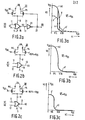
- Figure 1 shows a logic (NOR) gate circuit 10 which receives two input signals VI and VE at input terminals 11a, b and 12a, b respectively, and emits an output signal VO at the output terminal 13.
- the NOR gate is connected to a supply source (not shown) via supply source terminals D and S.
- the supply terminal D receives a supply voltage V DD (+5 V) and the terminal S receives a supply voltage V SS (0 V).
- the NOR gate 10 is composed of complementary insulated gate field effect transistors P1, P2, N1 and N2, preferably of MOS transistors, of which the transistors P1 and P2 are of the so-called P-type and the transistors N1 and N2 are of the N-type.
- the transistors N2 and P2 constitute a CMOS inverting circuit and receive at their gates the input signal.VI via the input terminals 11a, b.
- the gate circuit 10 will be able to respond to an input signal VI only when the second input signal VE (chip-enabling signal VE) is "low", as a result of which the transistor P1 becomes conducting and the transistor N1 is cut off.
- CMOS circuit has to be controlled by signals on TTL level (high level 2.0 V; low level 0.8 V) produced by TTL circuits, the circuit arrangement should be constructed very asymmetrically, which has the following disadvantages:
- the output signal of the inverting gate circuit is used to adapt the supply voltage to be applied to the gate circuit to the voltage levels of the input signals.
- Figure 2a shows an embodiment cfa circuit arrangement according to the invention.
- the supply voltage tapping point D is connected to main electrodes of the transistor means 30, the further main electrodes of which are connected to a supply source connection terminal DD.
- a first transistor N4 of the means 30 is of the N-type and has a gate electrode which is connected to the terminal DD.
- a second transistor P4 of the means 30 is of the P-type and its gate is connected to the output 22 of the inverting circuit 20.
- the means 30 are controlled via the inverting circuit 20 by the signal VO at the output 13 of the gate circuit 10, for which purpose the output 13 of the logic gate circuit 10 is connected to an input of a second CMOST inverting circuit 20.
- the transistor P4 is fully conducting and the supply voltage tapping point D of the gate circuit 10 is increased to the voltage V DD .
- the voltage VO will decrease from VDD to zero V, as is shown in Figure 3b, if the input signal VI at the input terminal 11 of the gate circuit 10 increases from zero V to V DD .
- the voltage tapping point D is then connected via the transistor N4 to the supply voltage V DD .
- the transistor N4 is connected as a load transistor. Since the transistor P4 is not in the conducting condition, the voltage at the tapping point D will no longer be increased to the voltage V DD.
- the voltage at the gate of the transistor P4 is continuously held at the potential V DD , as is shown in Figure 2c, the voltage at the tapping point D will be lower than the voltage at the tapping point D in Figure 2b. Therefore, by decreasing input voltage VI and V DD to zero V, the output voltage VO will increase from zero V to a value considerably lower than the voltage V DD (this value can be adjusted by the transistor N4).
- the voltage at the gate of the transistor P4 is not kept constant, however, because the voltage VO (see Figure 2a) decreases from V DD to V SS in dependence upon the output voltage VO at the output terminal 13. Initially, VO is equal to VDD and the transistor P4 is in the cut-off condition.
- the output voltage VO will initially vary (increase) according to the curve LE, as is shown in Figure 3c. However, as soon as the input voltage VI has fallen below V IH and decreases further to V IL , the output voltage VO will increase to such a level (1 V ⁇ VO ⁇ 2 V) that the output voltage VO at the output 22 decreases to such a level that the transistor P4 becomes conducting. This results in that the output voltage VO is increased to a slightly higher level, which of course leads to a further decrease of the output voltage VO of the inverter 20.
- FIG. 3a shows the curve L which follows the output voltage VO and which is composed of the low end LE and the high end HE of the curves of Figures 3c and 3b, respectively.
- Figure 3a indicates a further part L' of the curve of Figure 3a (by a broken line) to illustrate the influence of the selection of voltages which are applied to the voltage tapping point D.
- the gate circuit therefore has obtained a Schmitt trigger characteristic.
- FIG. 2d shows in detail the circuit arrangement of Figure 2a.
- the NOR gate 10 is identical to the NOR gate shown in Figure 1, although the P-type and N-type transistors of the gate 10 in Fig. 2d are constructed more symmetrically than the transistors in Figure 1 if the latter circuit is TTL-compatible.
- the inverting circuit 20 comprises two CMOS transistors P3 and N3, whose gates are connected to the input 21, which is connected to the output 13 of the NOR gate 10.
- the output 22 of the inverting circuit 20 is connected to the gate of the transistor P4 (P-type MOS transistor) of the transistor means 30.
- the transistor means 30 comprise a further transistor N4 (N-type MOS transistor), whose main electrodes are connected parallel to the main electrodes of the transistor P4.
- the gate of the transistor N4 is connected through the supply source connection terminal DD to the supply voltage V DD so that the transistor N4 acts as a load transistor.
- the invention is not limited to the embodiments described above, but can be used in principle in any complementary (insulated gate) field effect transistor circuit arrangement comprising inverting logic circuits, such as NAND, NOR ...
Landscapes
- Engineering & Computer Science (AREA)
- Computer Hardware Design (AREA)
- Physics & Mathematics (AREA)
- Computing Systems (AREA)
- General Engineering & Computer Science (AREA)
- Mathematical Physics (AREA)
- Power Engineering (AREA)
- Logic Circuits (AREA)
Applications Claiming Priority (2)
| Application Number | Priority Date | Filing Date | Title |
|---|---|---|---|
| NL8301711A NL8301711A (nl) | 1983-05-13 | 1983-05-13 | Complementaire igfet schakeling. |
| NL8301711 | 1983-05-13 |
Publications (1)
| Publication Number | Publication Date |
|---|---|
| EP0125733A1 true EP0125733A1 (fr) | 1984-11-21 |
Family
ID=19841852
Family Applications (1)
| Application Number | Title | Priority Date | Filing Date |
|---|---|---|---|
| EP84200673A Withdrawn EP0125733A1 (fr) | 1983-05-13 | 1984-05-10 | Circuit utilisant des transistors à effet de champ complémentaires à perte isolée |
Country Status (3)
| Country | Link |
|---|---|
| EP (1) | EP0125733A1 (fr) |
| JP (1) | JPS59212028A (fr) |
| NL (1) | NL8301711A (fr) |
Cited By (5)
| Publication number | Priority date | Publication date | Assignee | Title |
|---|---|---|---|---|
| EP0251383A2 (fr) * | 1986-06-25 | 1988-01-07 | Koninklijke Philips Electronics N.V. | Tampon d'entrée CMOS pour signaux TTL |
| FR2649265A1 (fr) * | 1989-06-30 | 1991-01-04 | Standard Microsyst Smc | Circuit amplificateur-separateur pour la conversion ttl-cmos |
| EP0546702A1 (fr) * | 1991-12-12 | 1993-06-16 | AT&T Corp. | Circuit tampon d'entrée CMOS à grande vitesse et faible consommation |
| EP0340282B1 (fr) * | 1987-10-14 | 1996-07-17 | Lsi Logic Corporation | Circuit d'attaque bimodal |
| US7119578B2 (en) * | 2003-11-24 | 2006-10-10 | International Business Machines Corp. | Single supply level converter |
Families Citing this family (1)
| Publication number | Priority date | Publication date | Assignee | Title |
|---|---|---|---|---|
| JP2692347B2 (ja) * | 1990-06-26 | 1997-12-17 | 松下電器産業株式会社 | 論理回路 |
Citations (11)
| Publication number | Priority date | Publication date | Assignee | Title |
|---|---|---|---|---|
| US3728556A (en) * | 1971-11-24 | 1973-04-17 | United Aircraft Corp | Regenerative fet converter circuitry |
| US3755690A (en) * | 1972-06-06 | 1973-08-28 | Standard Microsyst Smc | M.o.s. input circuit with t. t. l. compatability |
| US3904888A (en) * | 1974-05-17 | 1975-09-09 | Rca Corp | Circuits exhibiting hysteresis using transistors of complementary conductivity type |
| US3911289A (en) * | 1972-08-18 | 1975-10-07 | Matsushita Electric Ind Co Ltd | MOS type semiconductor IC device |
| US4032795A (en) * | 1976-04-14 | 1977-06-28 | Solitron Devices, Inc. | Input buffer |
| JPS54121051A (en) * | 1978-03-13 | 1979-09-19 | Nec Corp | Complementary mos field effect transistor circuit |
| JPS5648725A (en) * | 1979-09-28 | 1981-05-02 | Seiko Epson Corp | Mosfet circuit |
| FR2480531A1 (fr) * | 1980-04-15 | 1981-10-16 | Thomson Csf Mat Tel | Dispositif d'adaptation de niveau de signal d'entree, et circuit logique comportant un tel dispositif |
| JPS5781728A (en) * | 1981-09-14 | 1982-05-21 | Toshiba Corp | Integrated circuit device |
| JPS586620A (ja) * | 1981-07-03 | 1983-01-14 | Toshiba Corp | シユミツトトリガ回路 |
| US4437024A (en) * | 1981-10-22 | 1984-03-13 | Rca Corporation | Actively controlled input buffer |
-
1983
- 1983-05-13 NL NL8301711A patent/NL8301711A/nl not_active Application Discontinuation
-
1984
- 1984-05-10 EP EP84200673A patent/EP0125733A1/fr not_active Withdrawn
- 1984-05-11 JP JP59094401A patent/JPS59212028A/ja active Pending
Patent Citations (11)
| Publication number | Priority date | Publication date | Assignee | Title |
|---|---|---|---|---|
| US3728556A (en) * | 1971-11-24 | 1973-04-17 | United Aircraft Corp | Regenerative fet converter circuitry |
| US3755690A (en) * | 1972-06-06 | 1973-08-28 | Standard Microsyst Smc | M.o.s. input circuit with t. t. l. compatability |
| US3911289A (en) * | 1972-08-18 | 1975-10-07 | Matsushita Electric Ind Co Ltd | MOS type semiconductor IC device |
| US3904888A (en) * | 1974-05-17 | 1975-09-09 | Rca Corp | Circuits exhibiting hysteresis using transistors of complementary conductivity type |
| US4032795A (en) * | 1976-04-14 | 1977-06-28 | Solitron Devices, Inc. | Input buffer |
| JPS54121051A (en) * | 1978-03-13 | 1979-09-19 | Nec Corp | Complementary mos field effect transistor circuit |
| JPS5648725A (en) * | 1979-09-28 | 1981-05-02 | Seiko Epson Corp | Mosfet circuit |
| FR2480531A1 (fr) * | 1980-04-15 | 1981-10-16 | Thomson Csf Mat Tel | Dispositif d'adaptation de niveau de signal d'entree, et circuit logique comportant un tel dispositif |
| JPS586620A (ja) * | 1981-07-03 | 1983-01-14 | Toshiba Corp | シユミツトトリガ回路 |
| JPS5781728A (en) * | 1981-09-14 | 1982-05-21 | Toshiba Corp | Integrated circuit device |
| US4437024A (en) * | 1981-10-22 | 1984-03-13 | Rca Corporation | Actively controlled input buffer |
Non-Patent Citations (5)
| Title |
|---|
| ELECTRONICS, vol. 48, no. 15, 24th July 1975, pages 102-106, New York, US; S. HUME: "Consider 1,024-bit C-MOS RAMs for small static-memory systems" * |
| PATENT ABSTRACTS OF JAPAN, vol. 3, no. 143 (E-154), 27th November 1979, page 17 E 154; & JP-A-54 121 051 (NIPPON DENKI K.K.) 19-09-1979 * |
| PATENT ABSTRACTS OF JAPAN, vol. 5, no. 109 (E-65)[781], 15th July 1981; & JP-A-56 048 725 (SUWA SEIKOSHA K.K.) 02-05-1981 * |
| PATENT ABSTRACTS OF JAPAN, vol. 6, no. 164 (E-127)[1042], 27th August 1982; & JP-A-57 081 728 (TOKYO SHIBAURA DENKI K.K.) 21-05-1982 * |
| PATENT ABSTRACTS OF JAPAN, vol. 7, no. 80 (E-168)[1225], 2nd April 1983, page 7 E 168; & JP-A-58 006 620 (TOKYO SHIBAURA DENKI K.K.) 14-01-1983 * |
Cited By (9)
| Publication number | Priority date | Publication date | Assignee | Title |
|---|---|---|---|---|
| EP0251383A2 (fr) * | 1986-06-25 | 1988-01-07 | Koninklijke Philips Electronics N.V. | Tampon d'entrée CMOS pour signaux TTL |
| EP0251383A3 (fr) * | 1986-06-25 | 1988-07-13 | Koninklijke Philips Electronics N.V. | Tampon d'entrée CMOS pour signaux TTL |
| EP0340282B1 (fr) * | 1987-10-14 | 1996-07-17 | Lsi Logic Corporation | Circuit d'attaque bimodal |
| FR2649265A1 (fr) * | 1989-06-30 | 1991-01-04 | Standard Microsyst Smc | Circuit amplificateur-separateur pour la conversion ttl-cmos |
| EP0546702A1 (fr) * | 1991-12-12 | 1993-06-16 | AT&T Corp. | Circuit tampon d'entrée CMOS à grande vitesse et faible consommation |
| US5304867A (en) * | 1991-12-12 | 1994-04-19 | At&T Bell Laboratories | CMOS input buffer with high speed and low power |
| US7119578B2 (en) * | 2003-11-24 | 2006-10-10 | International Business Machines Corp. | Single supply level converter |
| CN1327510C (zh) * | 2003-11-24 | 2007-07-18 | 国际商业机器公司 | 单供电电平变换器 |
| US7336100B2 (en) | 2003-11-24 | 2008-02-26 | International Business Machines Corporation | Single supply level converter |
Also Published As
| Publication number | Publication date |
|---|---|
| NL8301711A (nl) | 1984-12-03 |
| JPS59212028A (ja) | 1984-11-30 |
Similar Documents
| Publication | Publication Date | Title |
|---|---|---|
| KR0136775B1 (ko) | 스위칭 유도 잡음을 감소시키는 출력 버퍼 | |
| JP2996301B2 (ja) | 負荷及び時間適応電流供給ドライブ回路 | |
| US6225846B1 (en) | Body voltage controlled semiconductor integrated circuit | |
| US4471242A (en) | TTL to CMOS Input buffer | |
| EP0107189A1 (fr) | Circuit trigger de Schmitt | |
| GB2184622A (en) | Output buffer having limited rate-of-change of output current | |
| EP1229649B1 (fr) | Circuit de sortie | |
| US7173473B2 (en) | Level-shifting circuitry having “high” output impedance during disable mode | |
| JPH06196992A (ja) | 半導体集積回路装置の出力回路 | |
| US3900746A (en) | Voltage level conversion circuit | |
| US6696858B2 (en) | Level-shifting circuit | |
| US4527081A (en) | Overshoot predriven semi-asynchronous driver | |
| US4808852A (en) | Input circuit having level shift | |
| US4894560A (en) | Dual-slope waveform generation circuit | |
| US4779015A (en) | Low voltage swing CMOS receiver circuit | |
| US5057720A (en) | Output buffering H-bridge circuit | |
| US5796281A (en) | Input buffer circuit with hysteresis for noise control | |
| US4237388A (en) | Inverter circuit | |
| US4933579A (en) | Output circuit for a semiconductor device for reducing rise time of an output signal | |
| EP0125733A1 (fr) | Circuit utilisant des transistors à effet de champ complémentaires à perte isolée | |
| US4488067A (en) | Tristate driver circuit with low standby power consumption | |
| US4717845A (en) | TTL compatible CMOS input circuit | |
| US5160857A (en) | Integratable transistor switch unit of the ntl logic family | |
| US5057713A (en) | Bipolar MOS logic circuit and semiconductor integrated circuit | |
| US4596939A (en) | Schmitt trigger input gate having delayed feedback for pulse width discrimination |
Legal Events
| Date | Code | Title | Description |
|---|---|---|---|
| PUAI | Public reference made under article 153(3) epc to a published international application that has entered the european phase |
Free format text: ORIGINAL CODE: 0009012 |
|
| AK | Designated contracting states |
Designated state(s): DE FR GB IT |
|
| STAA | Information on the status of an ep patent application or granted ep patent |
Free format text: STATUS: THE APPLICATION IS DEEMED TO BE WITHDRAWN |
|
| 18D | Application deemed to be withdrawn |
Effective date: 19850722 |
|
| RIN1 | Information on inventor provided before grant (corrected) |
Inventor name: FELLER, ERNST |