EP0124523B1 - Faseroptikschalter und diskret einstellbare verzögerungslinie - Google Patents
Faseroptikschalter und diskret einstellbare verzögerungslinie Download PDFInfo
- Publication number
- EP0124523B1 EP0124523B1 EP83900214A EP83900214A EP0124523B1 EP 0124523 B1 EP0124523 B1 EP 0124523B1 EP 83900214 A EP83900214 A EP 83900214A EP 83900214 A EP83900214 A EP 83900214A EP 0124523 B1 EP0124523 B1 EP 0124523B1
- Authority
- EP
- European Patent Office
- Prior art keywords
- fiber
- fibers
- plural
- coupling
- optical
- Prior art date
- Legal status (The legal status is an assumption and is not a legal conclusion. Google has not performed a legal analysis and makes no representation as to the accuracy of the status listed.)
- Expired - Lifetime
Links
Images


Classifications
-
- G—PHYSICS
- G02—OPTICS
- G02B—OPTICAL ELEMENTS, SYSTEMS OR APPARATUS
- G02B6/00—Light guides; Structural details of arrangements comprising light guides and other optical elements, e.g. couplings
- G02B6/24—Coupling light guides
- G02B6/26—Optical coupling means
- G02B6/28—Optical coupling means having data bus means, i.e. plural waveguides interconnected and providing an inherently bidirectional system by mixing and splitting signals
- G02B6/2804—Optical coupling means having data bus means, i.e. plural waveguides interconnected and providing an inherently bidirectional system by mixing and splitting signals forming multipart couplers without wavelength selective elements, e.g. "T" couplers, star couplers
- G02B6/2821—Optical coupling means having data bus means, i.e. plural waveguides interconnected and providing an inherently bidirectional system by mixing and splitting signals forming multipart couplers without wavelength selective elements, e.g. "T" couplers, star couplers using lateral coupling between contiguous fibres to split or combine optical signals
- G02B6/2826—Optical coupling means having data bus means, i.e. plural waveguides interconnected and providing an inherently bidirectional system by mixing and splitting signals forming multipart couplers without wavelength selective elements, e.g. "T" couplers, star couplers using lateral coupling between contiguous fibres to split or combine optical signals using mechanical machining means for shaping of the couplers, e.g. grinding or polishing
- G02B6/283—Optical coupling means having data bus means, i.e. plural waveguides interconnected and providing an inherently bidirectional system by mixing and splitting signals forming multipart couplers without wavelength selective elements, e.g. "T" couplers, star couplers using lateral coupling between contiguous fibres to split or combine optical signals using mechanical machining means for shaping of the couplers, e.g. grinding or polishing couplers being tunable or adjustable
-
- G—PHYSICS
- G02—OPTICS
- G02B—OPTICAL ELEMENTS, SYSTEMS OR APPARATUS
- G02B6/00—Light guides; Structural details of arrangements comprising light guides and other optical elements, e.g. couplings
- G02B6/24—Coupling light guides
- G02B6/26—Optical coupling means
- G02B6/28—Optical coupling means having data bus means, i.e. plural waveguides interconnected and providing an inherently bidirectional system by mixing and splitting signals
- G02B6/2804—Optical coupling means having data bus means, i.e. plural waveguides interconnected and providing an inherently bidirectional system by mixing and splitting signals forming multipart couplers without wavelength selective elements, e.g. "T" couplers, star couplers
- G02B6/2861—Optical coupling means having data bus means, i.e. plural waveguides interconnected and providing an inherently bidirectional system by mixing and splitting signals forming multipart couplers without wavelength selective elements, e.g. "T" couplers, star couplers using fibre optic delay lines and optical elements associated with them, e.g. for use in signal processing, e.g. filtering
Definitions
- the invention includes multiple optical fibers in a closely spaced side-by-side array on a substrate with an optical tap on each of the fibers.
- a second substrate with a tapped optical fiber is positioned in a face-to-face relationship with the first substrate. The second substrate is laterally adjusted so that the optical tap in the fiber on the second substrate may be selectively aligned with any one of the optical taps on the first substrate.
- the structure yields the optical equivalent of a single pole, multiple throw electrical switch which permits selective tapping of information into the fiber on the second substrate from any one of the fibers on the first substrate.
- the structure will selectively tap information from the fiber mounted on the second substrate into any one of the fibers mounted on the first substrate. If, in an alternative configuration, the first substrate mounts successive portions along the length of a single fiber, the apparatus forms a discretely variable fiber optic delay line.
- Fiber optic switches particularly for multi-mode fibers, are known in the art.
- switches are constructed by mounting multiple fibers on a first substrate such that cleaved or polished ends of the fibers are coplanar with one surface of the substrate.
- a second substrate mounts a fiber in a similar manner. The surfaces of the two substrates may be accurately transposed in order to align the butt end of the fiber in the second substrate with a selected one of the butt ends of the fibers in the first substrate, thus generating a switch. If such techniques were attempted with single-mode optical fibers, the degree of alignment required for low loss coupling would be extremely difficult to achieve.
- transversal filters capable of selectively filtering modulated light signals has been taught.
- construction of transversal filters by helically wrapping a single fiber optic element around a series of V-grooves in a silicon chip, with taps at each groove, is known in the art.
- the frequency versus attenuation characteristics of prior transversal filters was, of necessity, determined at the time of construction of the filter. There is, therefore, a need for an adjustable fiber optic delay line so that, for example, the frequency response of a transversal filter utilizing the delay line may be adjusted.
- a fiber optic discretely variable delay line comprising a first single mode optical fiber, a second single mode optical fiber, the second fiber having plural taps, spaced at predetermined intervals along the second fiber, each capable of coupling a lightwave from the second fiber to the first fiber, and means for selectively positioning the first fiber to provide optical coupling with a selected one of the plural taps of the second fiber, to control the transmission time of the lightwave through the second fiber, and provide a discretely variable delay for the lightwave.
- a method of making a tapped delay line with a discretely variable time delay comprising the step of providing first and second single mode optical fibers, the step of removing a portion of the cladding from plural selected locations along the first fiber to provide respective- plural evanescent field coupling regions, the step of removing a portion of the cladding from a selected location along the second fiber to provide an evanescent field coupling region, and the step of adjustably mounting the fibers for selective juxtaposition of the second fibers coupling region and any one of the plural first fiber coupling regions.
- a fiber optic frequency filter comprising a first single mode optical fiber, a portion of which includes plural taps, spaced at predetermined intervals along the first fiber portion, a second single mode optical fiber, first means for optically coupling the second fiber to a selected one of the plural taps of the first fiber at a first predetermined location on the second fiber, second means for optically coupling the first and second fibers at a first predetermined location on the first fiber, removed from the first fiber portion and at a second predetermined location on the second fiber, and means for adjusting the fiber coupling means to couple the fibers at another of the plural taps to vary the frequency response of the filter.
- a method of frequency filtering comprising the step of providing first and second optical fibers, a portion of said first fiber having plural taps, spaced at predetermined intervals along the first fiber, the step of relatively positioning the optical fibers to provide optical coupling between the first and second fibers at one of the plural taps, the step of optically coupling the first fiber to the second fiber at a predetermined location removed from the plural taps, the step of introducing a modulated lightwave into one of the signal mode fibers to provide an optical output signal in the other of the single mode fibers, the output single being comprised of light modulated at first and second frequencies, and the step of relatively positioning the first and second optical fibers to provide optical coupling at another of the plural taps selected to pass the portion of optical output signal at the first frequency, while attenuating the portion of the optical output signal at the second frequency.
- the structure of the preferred embodiment of this invention comprises a plurality of single-mode optical fibers mounted in a side-by-side array in parallel v-grooves in a plate or chip.
- these optical fibers are independent of one another.
- the fibers are successive lengths of a single optical fiber which is wrapped around the plate or chip so that successive portions are in adjacent v-grooves. A portion of the cladding on each optical fiber mounted on the plate or chip is removed along a lateral line normal to the length of the fiber in the v-grooves, thereby simultaneously creating a tap in each fiber.
- Light is selectively detected from one of the taps by superimposing, on the plate or chip, a second v-grooved plate or chip which supports a single optical fiber, the cladding of which has been similarly removed.
- a second v-grooved plate or chip which supports a single optical fiber, the cladding of which has been similarly removed.
- evanescent field coupling occurs between the fiber on the second plate or chip and a selected one of the fibers on the first plate or chip. This selection depends upon the relative position of the two plates.
- By adjusting the lateral position of the second plate with reference to that of the first light can be selectively coupled between the tapped area of the fiber in the second substrate and any one of the tapped fibers in the first substrate.
- the optical fibers on the first plate are preferably mounted so that the distances between successive fibers is identical.
- the level at which the plural fibers are mounted on the plate, at the location where they are to be tapped, is identical, since the taps are made by lapping a portion of the cladding from each of the fibers simultaneously.
- the taps can be identically formed.
- the plate is a silicon chip having etched parallel grooves. It is possible to etch silicon chips by using photolithographic methods and to thereby obtain a high degree of accuracy.
- the second plate is formed as a quartz block including a v-groove but may alternatively be formed as an etched silicon substrate.
- Single-mode optical fibers generally have a core diameter of a few microns and a cladding diameter in a range of one hundred microns along with an outer cover.
- the outer cover is removed and the cladding is secured to the v-groove to permit accurate location of the core and to thereby permit polishing of the fibers to within a few mircons of the core.
- the coupling technique provided by this switch is described as evanescent field coupling. It is, therefore, important that the amount of material removed from the fiber cladding be controlled so that the spacing between the core portions of abutted fiber optic strands be within a predetermined critical zone.
- each strand to receive a significant portion of the evanescent field energy from the other strand, so that coupling is achieved without significant energy loss.
- the amount of coupling between the two fibers is determined by the distance between the fiber cores. Additionally, the amount of coupling can be varied by moving one of the cores laterally with respect to the other so that the cores are somewhat out of alignment.
- the coupling . between fibers in an evanescent field coupler of the type described herein is far less sensitive to lateral misalignment than would be the case where the fibers are butt-coupled.
- the switch of the present invention provides adequate coupling even in the case where the optical fiber cores are misaligned by several microns, a situation which would destroy the effectiveness of the butt-coupled switch described earlier.
- the present invention provides a practical switch and, furthermore, provides a practical, discretely variable delay line not heretofore possible.
- an evanescent coupler 10 includes two strands 12a and 12b of a single-mode fiber optic material mounted in longitudinal arcuate grooves 13a and 13b, respectively, formed in optically flat, confronting surfaces 14a and 14b, respectively, of rectangular bases or blocks 16a and 16b, respectively.
- the block 16a with the strand 12a mounted in the groove 13 will be referred to as the coupler half 10a
- the block 16b with the strand 12B mounted in the groove 13b will be referred to as the coupler half 10b.
- Each of the strands 12a and 12b comprises a commercially available fiber of quartz glass which is doped to have a central core and an outer cladding. It will be seen below that the present invention is particularly advantageous for use with single-mode fibers, which typically have a core diameter on the order of 10 microns or less and a cladding diameter on the order of 125 microns, although the invention may also be employed with other types of fibers, such as multi-mode fibers. In the embodiment disclosed, single mode fibers are utilized, however, for clarity of illustration, the diameter of the strands 12 and their respective cores are exagerated. Furthermore, test results described herein are for couplers utilizing single mode fibers.
- the arcuate grooves 13a and 13b have a radius of curvature which is very large compared to the diameter of the fibers 12, and have a width slightly larger than the fiber diameter to permit the fibers 12, when mounted therein, to conform to a path defined by the bottom walls of the grooves 13.
- the depth of the grooves 13a and 13b varies from a minimum at the center of the blocks 16a and 16b, respectively, to a maximum at the edges of the blocks 16a and 16b, respectively.
- the grooves 13 are illustrated as being rectangular in cross-section, however, it will be understood that other suitable cross-sectional contours which will accommodate the fibers 12 may be used alternatively, such as a U-shaped cross-section or a V-shaped cross-section. Techniques for forming the grooves 13 and mounting the fibers 12 therein are discussed below.
- the depth of the grooves 13 which mount the strands 12 is less than the diameter of the strands 12, while at the edges of the blocks 16, the depth of the grooves 13 is preferably at least as great as the diameter of the strands 12.
- Fiber optic material was removed from each of the strands 12a and 12b to form the respective oval-shaped planar surfaces 18a, 18b, which are coplanar with the confronting surfaces 17a, 17b, respectively. These surfaces 18a, 18b will be referred to herein as the fiber "facing surfaces”. It will be understood that these facing surfaces provide a coupling area or region for the fibers 12a and 12b.
- the amount of fiber optic material removed increases gradually from zero towards the edges of the block 16 to a maximum towards the center of the block 16.
- This tapered removal of the fiber optic material enables the fibers to converge and diverge gradually, which is advantageous for avoiding backward reflection and excess loss of light energy.
- the coupler halves 10a and 10b are identical, and are assembled by placing the confronting surfaces 14a and 14b of the blocks 16a and 16b together, so that the facing surfaces 18a and 18b of the strands 12a and 12b are in facing relationship.
- index matching substance such as index matching oil, is provided between the confronting surfaces 14.
- This substance has a refractive index approximately equal to the refractive index of the cladding, and also functions to prevent the optically flat surfaces 14 from becoming permanently locked together.
- the oil is introduced between the blocks 16 by capillary action.
- An interaction or coupling region 32 is formed at the junction of the strands 12, in which light is transferred between the strands by evanescent field coupling. It has been found that, to insure proper evanescent field coupling, the amount of material removed from the fibers 12 must be carefully controlled so that the spacing between the core portions of the strands 12 is within a predetermined "critical zone".
- the evanescent fields extend into the cladding and decrease rapidly with distance outside their respective cores. Thus, sufficient material should be removed to permit each core to be positioned substantially within the evanescent field of the other. If too little material is removed, the cores will not be sufficiently close to permit the evanescent fields to cause the desired interaction of the guided modes, and thus, insufficient coupling will result.
- each stand receives a significant portion of the evanescent field energy from the other strand, and optimum coupling is achieved without significant energy loss.
- the critical zone is illustrated schematically in Figure 5 as including that area, designated by the reference numeral 33, in which the evanescent fields, designated by reference numerals 34a and 34b, of the fibers 12a and 12b, respectively, overlap with sufficient strength to provide coupling, i.e., each core is within the evanescent field of the other.
- mode perturbation occurs within the area 33 when the cores are brought too close together.
- the critical zone is defined as that area in which the evanescent field 34 overlap with sufficient strength to cause coupling without substantial mode perturbation induced power loss.
- the critical zone for a particular coupler is dependent upon a number of interrelated factors such as the parameters of the fiber itself and the geometry of the coupler. Further, for a single mode fiber having a step-index profile, the critical zone can be quite narrow. In a single mode fiber coupler of the type shown in Figures 1-4, for example, the required center-to-center spacing between the strands 12 at the center of the coupler is typically less than a few (e.g., 2-3) core diameters.
- the strands 12a and 12b are (1) identical to each other, (2) have the same radius of curvature at the interaction region 32, and (3) have an equal amount of fiber optic material removed thereform to form their respective facing surfaces 18a and 18b.
- the fibers 12 are symmetrical, through the interaction region 32, in the plane of the facing surfaces 18, so that the facing surfaces 18 are coextensive if superimposed. This insures that two fibers 12a and 12b will have the same propagation characteristics at the interaction region 32, and thereby avoids coupling attenuation associated with dissimilar propagation characteristics.
- the blocks or bases 12 may be fabricated of any suitable rigid material.
- the bases 12 comprise generally rectangular blocks of fused quartz glass approximately one inch long, one inch wide, and 0.4 inches thick.
- the fiber optic strands 12 are typically secured in the slots 13 by suitable cement 38, such as epoxy glue.
- suitable cement 38 such as epoxy glue.
- One advantage of the fused quartz blocks 16 is that they have a coefficient of thermal expansion similar to that of glass fibers, and this advantage is particularly important if the blocks 16 and fibers 12 are subjected to any heat treatment during the manufacturing process.
- Another suitable material for the block 16 is silicon, which also has excellent thermal properties for this application.
- the coupler 10 includes four ports, labeled A, B, C, and D in Figure 1.
- ports A and C which correspond to strands 12a and 12b, respectively, are on the lefthand side of the coupler 10
- the ports B and D which correspond to the strands 12a and 12b, respectively, are on the righthand side of the coupler 10.
- input light of a suitable wavelength e.g., 1.15 microns
- This light passes through the coupler and is output at port B and/or port D, depending upon the amount of power that is coupled between the strands 12.
- the term "normalized coupled power" is defined as the ratio of the coupled power to the total output power.
- the normalized coupled power would be equal to the ratio of the power at port D to the sum of the power output at ports B and D. This ratio is also referred to as the "coupling efficiency", and when so used is typically expressed as a percent.
- the term "normalized coupled power” it should be understood that the corresponding coupling efficiency is equal to the normalized coupled power times one-hundred.
- tests have shown that an evanescent coupler 10 may have a coupling efficiency of up to one-hundred percent. However, it will also be seen that the coupler 10 may be "tuned” to adjust the coupling efficiency to any desired value between zero and the maximum.
- an evanescent coupler 10 is highly directional, with substantially all of the power applied at one side of the coupler being delivered to the other side of the coupler.
- the coupler directivity is defined as the ratio of the power at port D to the power at port C, with the inut applied to port A. Tests have shown that the directionally coupled power (at port D) is greater than 60 dB above the contradirectionally coupled power (at port C).
- the coupler directivity is symmetrical. That is, the coupler operates with the same characteristics regardless of which side of the coupler is the input side and which side is the output side. Moreover, the coupler 10 achieves these results with very low throughput losses.
- the throughput loss is defined as the ratio of the total output power (ports B and D) to the input power (port A), subtracted from one (i.e., 1-(P B +Pp)/P A ).
- the coupler 10 operates on evanescent field coupling principles in which guided modes of the strands 12 interact, through their evanescent fields, to cause light to be transferred between the strands 12. As previously indicated, this transfer of light occurs at the interaction region 32. The amount of light transferred is dependent upon the proximity and orientation of the cores, as well as the effective length of the interaction region 32. The length of the region 32 is, in turn, dependent upon the radius of curvature of the fibers 12, and, to a limited extent, the core spacing, although it has been found that the effective length of the interaction region 32 is substantially independent of core spacing.
- the radius of curvature is on the order of 25 centimeters, and the effective interaction region is approximately one millimeter long at a signal wavelength of 633 nm.
- the light makes only one transfer between the strands 12 as it travels through the interaction region 32.
- a phemomenon referred to herein as "overcoupling” will occur, in which the light will transfer back to the strand from which it originated.
- the light may make multiple transfers back and forth between the two strands 12 and it travels through the region 32, the number of such transfers being dependent on the length of the interaction region 32, and the core spacing.
- FIG. 6 shows a schematic representation of the coupler 10 of Figure 1.
- the cores of fibers 12a and 12b are shown as gradually converging to a minimum spacing, labeled H, at the center of the coupler and diverging towards the edges of the coupler.
- the effective interaction length is labeled L and the radius of curvature of the strands 12a and 12b is labeled R.
- L is a function of the radius of curvature R, it is substantially independent of the minimum spacing H between the fibers 12.
- Figure 8 shows a sinusoidal curve 40 which illustrates that the coupled power Pc varies sinusoidally as a function of the interaction length L for a given fiber spacing H1.
- the coupled power is approximately fifty-percent when the interaction length is equal to L1, and increases to one-hundred-percent when the interaction length increases to L2.
- "overcoupling" results, in which light is transferred back to the strand from which it originated, and the coupled power PC begins to decrease towards zero.
- the coupled power then increases from zero to, for example, fifty percent at L3.
- the amount of coupling may be varied by changing the effective length of the interaction region.
- the effect of decreasing the spacing H between the fibers is to increase the strength of the coupling, and thus, increase the amount of light transferred over a given interaction length L, as shown by comparing the sinusoidal curve 42 of Figure 9 with the sinusoidal curve of Figure 8.
- the coupled power may be one-hundred percent at interaction length L1 in Figure 9, as compared to fifty percent for the same interaction length L1 in Figure 8.
- the curve 42 then begins to demonstrate overcoupling and the coupled power decreases to fifty percent at interaction length L2.
- the curve 42 indicates that the coupled power is again one-hundred percent.
- the amount of power coupled may be adjusted by changing the fiber core spacing.
- the relationship between the minimum fiber spacing H and the coupled power P c for a given interaction length L is illustrated in Figure 10 by the curve 44.
- L i.e., radius of curvature
- the normalized coupled power oscillates between 0 and 1 with increasing frequency or the core spacing H decreases.
- the reference points a, b, and c on the curve H were chosen somewhat arbitrarily to indicate normalized coupled power of 0.5, 1.0, and .25, respectively. It will be recognized that at point "a" fifty percent of the power is coupled from one to the other. At point “b” full coupling is achieved, and one-hundred percent of the optical power is transferred between the strands.
- Point "c" represents an overcoupled condition wherein the coupled power has decreased from full coupling to twenty-five percent.
- the term “tuning” is defined as translating the fibers 12 relative to each other to adjust the power coupled therebetween. Such translation of the fibers 12 is accomplished by sliding the planar facing surfaces 18 relative to each other, so that they are offset, rather than superimposed. That is, the fibers 12 are mutually displaced in the plane of the planar facing surfaces. Viewed another way, such translation occurs when respective planes in which each of the fibers lie, are displaced relative to each other.
- the facing surfaces 18 are offset laterally.
- laterally offset means sliding the facing surfaces 18 laterally from their superimposed position to increase the spacing between the fiber cores, while maintaining a substantially parallel relationship between the fibers 12.
- Such lateral offset of the facing surfaces 18 is illustrated schematically in Figure 11. The effect of such lateral offset is, of course, to change the spacing between the cores of the fibers 12.
- the curve 46 of Figure 12 graphically illustrates the effect of laterally offsetting the fiber facing surfaces 18 for a coupler having a minimum edge-to-edge core spacing H equal to "a" ( Figure 10).
- the normalized coupled power will be equal to 0.5, as required by the curve 44 of Figure 10.
- the facing surfaces of the fibers 12 are laterally offset in either direction to increase the spacing between the cores, the coupled power gradually decreases to zero.
- the curve 50 of Figure 14 shows coupled power as a function of relative fiber offset for a core spacing equal to "c" ( Figure 10), which, as will be recalled, represents an overcoupled condition. From this curve 50, it may be seen that, when the facing surfaces 18 of the fibers 12 are superimposed, the normalized coupled power is 0.25. As the core spacing is increased by sliding the facing surfaces 18 so that they are laterally offset, the normalized coupled power initially increases to 1.0 and then decreases toward zero when the core spacing is further increased.
- the two horizontal broken lines drawn through the center of Figure 14 provide the upper and lower boundaries of an 0.2 dB power loss band. It may be seen that the power loss curve 60 is within this band for lateral offsets up to about 12 microns in either direction. Further, it may be seen that, at a 12-micron lateral offset, the normalized coupled power is approximately 0.1. Thus, for coupled power between 0.1 and 1, the power loss is within about 0.2 dB of the minimum power loss. If the power loss band is expanded to 0.5 dB, the power loss band is within the 0.5-dB band for fiber offsets of up to 15 microns, which corresponds to a coupled power of less than 0.05 (i.e., 5 percent).
- this coupler exhibits substantially constant throughput losses, i.e., within a relatively narrow power loss band width, throughout substantially the entire operating range of the device. Further, it is significant that the throughput losses are very low, and relatively constant for coupled power between ten percent and one-hunded percent.
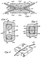
- FIG. 16 and 17 shows plural optical fibers 64 mounted on a chip 66 with individual v-grooves 68 to receive each optical fiber 64. Taps are formed by simultaneously polishing the fibers and the chip 66, so that each of the optical fibers 64 is tapped at a lateral line 70. Before a description of the manner of formation of the taps on the optical fibers 64, it is necessary to describe the construction of the chip 66 and the manner by which the optical fibers 64 are laid in the v-grooves 68 in the chip 66.
- each of these v-grooves 68 be identical in width and depth, since the fibers are to be coplanar because the taps in the fibers in these v-grooves will be constructed simultaneously. If the v-grooves are identical, the taps on the fibers will have uniform characteristics. Because of this need for great precision in the construction of the v-grooves, the preferred material for the chip 66 is silicon, which can be etched by photolithographic techniques, rather than some other material in which grooves are machined.
- the type of silicon used is commercially available 100 oriented silicon, because when the surface of this type of silicon is subjected to an etching solution, the surface dissolves at an angle theta, as shown in Figure 18. For 100 oriented silicon the angle theta is 54.74 degrees.
- the following photolithographic method may be used.
- the chip 66 is first heated so that a very thin oxide layer 72 will cover the chip 66, as shown in Figure 19.
- the chip 66 is then coated with a photosensitive coating 74 known as photoresist.
- a mask 80 is then placed over the chip, and the top of the chip is exposed to ultraviolet light.
- positive-acting photoresist is used, so the portions of the photoresist 74 under the opaque sections of the mask 80 will be left to perform the masking function.
- the next step is to etch away the photoresist 74 and oxide layer 72 which were under the non- opaque portions of the mask 80 by using a buffered hydrochloric acid solution.
- the remaining photoresist is then stripped by use of a special solvent, and the chip 66 will appear as it does in Figure 20, covered by a mask of the oxide layer 72.
- the silicon wafer 66 is then placed into an anisotropic etching solution, commonly potassium hydroxide solution.
- the portions of the chip not covered by the oxide layer 72 will then be dissolved by the etching solution at an angle of 54.74 degrees from the surface 76 of the chip 66.
- the etch will develop as a flat-bottom groove until the two angled planes intersect and a true v-groove is formed, as shown in Figure 18.
- This photolithographic technique is well-known in the art, and has been used extensively in the manufacture of semiconductors.
- optical fiber There are two widely-used types of single mode optical fiber, one manufactured by ITT which has a diameter of about 80 microns (400 microns including the plastic jacket), and a second brand of fiber manufactured by Corning which is 125 microns in diameter (135 microns with the lacquer jacket). Which of these or other fibers, is used depends on the wavelength of the light to be used; if visible light is to be used, the ITT fiber is acceptable since it is single mode at visible light wavelengths (longer than green); and if infrared light is to be used, the Corning fiber is acceptable since it is single mode at infrared wavelengths.
- the silicon chip 66 is mounted on a block of quartz 70 which has a curved upper surface 72. It has been found that a silicon chip 66 of standard thickness (0.25 millimeter) and about three-centimeter length can be bent without breaking around a twelve-inch radius. An adhesive substance such as wax is used to hold the silicon chip 66 on the quartz block 70 in the curved configuration shown in Figure 16.
- the portions of the optical fibers 64 which are to be mounted in the v-grooves 68 preferably have the protective jacket removed.
- the ITT fiber has a plastic jacket which may be removed by dipping it in sulfuric acid. The resiliency of the plastic jacket prevents precision in the lapping operation, so it should be removed.
- the Corning fiber has a lacquer jacket which may be removed by dipping it in acetone. Since the lacquer jacket is more solid than the plastic jacket, its removal is preferential rather than mandatory.
- the next step is to lap the upper surface of the optical fibers 64 at the lateral line 70.
- This lapping operation will remove a portion of the cladding 79, as best shown in Figure 17. It is important to note that not all of the cladding material 76 around the core 78 of the optical fiber 64 is to be removed. The distance between the core 78 and the lapped surface 82 depends on the characteristics of the coupler to be formed, in accordance with the previous description.
- the quartz block 70 advantageously includes plural. spacing elements 22 which are used to stabilize the chip 66 during polishing and to provide a bearing surface for the second half of the switch.
- the second half of the switch is preferably formed of a quartz block 91 including a groove 93 as earlier described for a standard coupler.
- the groove 83 has a relatively large radius of curvature, peaking at the center of the substrate 91.
- An optical fiber 95 is placed within the groove 93 and secured using epoxy or any other satisfactory adhesive. This fiber is then lapped at the highest point of the curve along with the surface of the quartz block 91 to yield a planar surface for the cladding, which is a few microns separated from the core of the fiber, and which is co-planar with the surface of the quartz block 91.
- the index matching oil is then placed on the polished flat surface 82 of the silicon substrate 66.
- the index matching oil advantageously has an index of refraction slightly lower than that of the cladding 79 of the fiber elements 64 and the fiber cores 78 themselves to prevent loss of light outside of the coupling area.
- the construction shown in Figure 16 provides an optical switch. Switching is accomplished by aligning the core of the upper fiber 95 with the desired lower fiber 64 core.
- an operator merely adjusts the position of the upper quartz block 91 in the lateral direction (arrow 97) relative the axis of the fiber 95 with respect to the lower substrate 66 so that the upper fiber 95 is in alignment with the desired lower fiber 64.
- Adjustable coupling with respect to each of the fibers 64 can be obtained by positioning the upper substrate 91 such that the fiber 95 is slightly offset from the selected fiber 64.
- coupling can be varied by orienting the upper fiber 95 at an angle with respect to the desired lower fiber 64.
- the distance from the top flat face 82 of the fiber cladding 79 and the fiber core 78 may be slightly different for different fibers 64. This would yield a different coupling ratio for the various fibers 64.
- the coupling ratio can be maintained constant at each switch position.
- Figure 21 shows a fixture for permitting accurate adjustment of the upper substrate 91 with respect to the lower substrate 66 to accomplish the prevously described switching function.
- the quartz block 70 is fixed in a lower trough created by a pair of walls 102 and 104 of a frame 106.
- the wall 104 is slightly lower in height than the edge of the block 70 of the switch.
- a pair of ledges 108 above the walls 102 and 104 are wide enough to permit at least half the width of the substrate 91 to slide over them.
- An upper wall 110 supports two spring members 112 which maintain the upper substrate 91 biased away from the wall 110.
- a pair of micrometers 114 and 116 are mounted in the frame 106.
- the micrometer 114 bears upon the upper substrate 91 of the switch against a spring 112 and is adjusted to change the optical coupling from one fiber 64 to a different fiber 64.
- the micrometer 114 is centrally located on the side of the substrate 91 to permit this lateral adjustment without rotation of the substrate 91.
- the micrometer 116 is offset on the upper substrate 91 so that it can be used to adjust the angular orientation of the upper substrate 91 with respect to the lower substrate 70.
- the upper substrate 91 of the optical delay line is made of quartz and has a v-groove 93 with a fiber 95 secured therein. This fiber is lapped to within a few microns of its core, just as the fiber in the switch.
- the lower portion is formed with a quartz base 70 and a v-groove silicon substrate 66.
- the major difference is that there is only a single fiber 121 which is wrapped in helical fashion around the base 70 of the delay line.
- the first loop of fiber 121 is placed in the first v-groove 68.
- the next loop is placed in the next v-groove 68, and so on until all the v-grooves 78 are filled.
- Figure 23 shows a graph of exemplary possible delays in the case of a 7-loop delay line of the type described above.
- the first graph shows the time at which an input light pulse is introduced into the fiber 121.
- the shortest delay is provided by aligning the upper fiber 95 with the tapped portion of the fiber 121 closest to the light source, and is illustrated in the next lower graph.
- the next three graphs depict the output of the delay line when the upper fiber 95 is aligned, respectively, with loops 3, 5 and 7 of the fiber 121. It can be seen that the difference between the delay at the first tap on the fiber 121 and the delay at the third tap on the fiber 121 is approximately 5 nanoseconds.
- FIG 24 shows schematically the use of the variable delay line of this invention in a tuneable filter.
- a modulated light source is shown as a laser diode input 123.
- Light from the diode 123 is coupled to the fiber 95 on the upper substrate 91 ( Figure 22) of the adjustable delay line.
- Each of the coupling points 125 along the length of the fiber 121 of the variable delay line provides a different delay as previously described.
- Fiber 95 can be adjusted to couple at any of the coupling points 125.
- the fibers 95 and 121 are polished so that the amount of coupling at each of these points 125 is 3DB.
- Fibers 95 and 121 extend through another 3DB directional coupler 124 which acts to recombine the two light signals for detection by a detector 129.
- the filter shown in Figure 24 has an impulse response consisting of two equal pulses separated in time by the relative delay nT-P where T is the delay of each loop between successive taps 125, n is the number of the loops between the coupling point 125 which is aligned with the fiber 95 and the coupler 127 and P is the difference in delay between the fibers connecting the coupler 127 to the coupling point on the fiber 95 and the last tap 125 of the fiber 121.
- the filter in Figure 24 will have this transfer characteristic provided the coherence length of the source 123 is short compared to the delay difference nT-P.
- Figures 25A-25C show the frequency response of the filter of Figure 24.
- the upper trace in these figures is the frequency response of the laser diode 123 and the detector 129.
- the lower trace in Figure 25A is the response for the minimum relative delay of 0.6 nanoseconds.
- the maximum delay in such discretely variable delay lines can be made very large since the attenuation and dispersion of optical fibers is low.
- the minimum delay between taps is limited to about 100 picoseconds by bending loss around the loop and by fabrication considerations.
Landscapes
- Physics & Mathematics (AREA)
- General Physics & Mathematics (AREA)
- Optics & Photonics (AREA)
- Engineering & Computer Science (AREA)
- Signal Processing (AREA)
- Theoretical Computer Science (AREA)
- Light Guides In General And Applications Therefor (AREA)
- Optical Couplings Of Light Guides (AREA)
- Networks Using Active Elements (AREA)
- Mechanical Light Control Or Optical Switches (AREA)
- Ultra Sonic Daignosis Equipment (AREA)
- Mechanical Coupling Of Light Guides (AREA)
- Keying Circuit Devices (AREA)
- Electronic Switches (AREA)
Claims (13)
Priority Applications (1)
| Application Number | Priority Date | Filing Date | Title |
|---|---|---|---|
| AT83900214T ATE50071T1 (de) | 1982-11-12 | 1982-11-12 | Faseroptikschalter und diskret einstellbare verzoegerungslinie. |
Applications Claiming Priority (1)
| Application Number | Priority Date | Filing Date | Title |
|---|---|---|---|
| PCT/US1982/001608 WO1984002005A1 (en) | 1982-11-12 | 1982-11-12 | Fiber optic switch and discretely variable delay line |
Publications (3)
| Publication Number | Publication Date |
|---|---|
| EP0124523A1 EP0124523A1 (de) | 1984-11-14 |
| EP0124523A4 EP0124523A4 (de) | 1985-06-26 |
| EP0124523B1 true EP0124523B1 (de) | 1990-01-31 |
Family
ID=22168373
Family Applications (1)
| Application Number | Title | Priority Date | Filing Date |
|---|---|---|---|
| EP83900214A Expired - Lifetime EP0124523B1 (de) | 1982-11-12 | 1982-11-12 | Faseroptikschalter und diskret einstellbare verzögerungslinie |
Country Status (13)
| Country | Link |
|---|---|
| US (1) | US4723827A (de) |
| EP (1) | EP0124523B1 (de) |
| JP (1) | JPS60500030A (de) |
| KR (1) | KR840006704A (de) |
| AT (1) | ATE50071T1 (de) |
| AU (1) | AU558937B2 (de) |
| BR (1) | BR8208104A (de) |
| CA (1) | CA1251072A (de) |
| DE (1) | DE3280098D1 (de) |
| IL (1) | IL69969A (de) |
| IT (1) | IT1168229B (de) |
| NO (1) | NO842831L (de) |
| WO (1) | WO1984002005A1 (de) |
Families Citing this family (48)
| Publication number | Priority date | Publication date | Assignee | Title |
|---|---|---|---|---|
| GB8706929D0 (en) * | 1987-03-24 | 1987-04-29 | British Telecomm | Optical coupling device |
| US4991922A (en) * | 1988-08-29 | 1991-02-12 | The Charles Stark Draper Laboratory, Inc. | Optical fiber coupler and method |
| US4934777A (en) * | 1989-03-21 | 1990-06-19 | Pco, Inc. | Cascaded recirculating transmission line without bending loss limitations |
| US5109449A (en) * | 1989-03-27 | 1992-04-28 | Hughes Aircraft Company | Variable optical fiber delay line |
| BE1005172A3 (nl) * | 1991-08-09 | 1993-05-11 | Bell Telephone Mfg | Konstruktie voor het optisch koppelen, substraat daarvoor en werkwijze voor het verwezenlijken van dergelijke konstruktie. |
| US7106917B2 (en) | 1998-11-13 | 2006-09-12 | Xponent Photonics Inc | Resonant optical modulators |
| US6516114B2 (en) * | 2000-06-27 | 2003-02-04 | Oluma, Inc. | Integration of fibers on substrates fabricated with grooves |
| US6501875B2 (en) * | 2000-06-27 | 2002-12-31 | Oluma, Inc. | Mach-Zehnder inteferometers and applications based on evanescent coupling through side-polished fiber coupling ports |
| US6625349B2 (en) * | 2000-06-27 | 2003-09-23 | Oluma, Inc. | Evanescent optical coupling between a waveguide formed on a substrate and a side-polished fiber |
| US6597833B1 (en) * | 2000-06-27 | 2003-07-22 | Oluma, Inc. | Wavelength-division multiplexers and demultiplexers based on mach-zehnder interferometers and evanescent coupling |
| US6621951B1 (en) * | 2000-06-27 | 2003-09-16 | Oluma, Inc. | Thin film structures in devices with a fiber on a substrate |
| US6490391B1 (en) * | 2000-07-12 | 2002-12-03 | Oluma, Inc. | Devices based on fibers engaged to substrates with grooves |
| US6621952B1 (en) * | 2000-08-10 | 2003-09-16 | Oluma, Inc. | In-fiber variable optical attenuators and modulators using index-changing liquid media |
| US6571035B1 (en) * | 2000-08-10 | 2003-05-27 | Oluma, Inc. | Fiber optical switches based on optical evanescent coupling between two fibers |
| US6542663B1 (en) * | 2000-09-07 | 2003-04-01 | Oluma, Inc. | Coupling control in side-polished fiber devices |
| US6658176B2 (en) * | 2000-09-29 | 2003-12-02 | Sarnoff Corporation | Optical switch using movable micromechanical cantilevers and evanescent coupling |
| WO2002050575A2 (en) * | 2000-12-21 | 2002-06-27 | Cquint Communications Corporation | Resonant optical modulators |
| KR100416688B1 (ko) * | 2001-11-08 | 2004-01-31 | 주식회사 한택 | 광소자가 집적된 광섬유 블럭 |
| US6640028B1 (en) | 2001-11-30 | 2003-10-28 | General Dynamics Advanced Technology Systems, Inc. | Bend-type fiber optic light injector |
| US6665469B1 (en) | 2002-01-02 | 2003-12-16 | General Dynamics Advanced Information Systems, Inc. | Light injector/extractor for multiple optical fibers |
| US6819831B1 (en) | 2002-03-04 | 2004-11-16 | Kenneth R. Schroll | Adjustable, reconfigurable, multi-port optical fiber coupler |
| US6968103B1 (en) * | 2002-10-10 | 2005-11-22 | General Dynamics Advanced Information Systems, Inc. | Optical fiber coupler and method for making same |
| US7146069B1 (en) | 2003-06-05 | 2006-12-05 | Calient Networks, Inc. | Optical system for selectable delay |
| KR20050109370A (ko) * | 2004-05-15 | 2005-11-21 | 엘지전자 주식회사 | 집적광학형 실시간 지연 장치 및 그 제조 방법 |
| US7802928B2 (en) * | 2008-01-04 | 2010-09-28 | Honeywell International Inc. | System and method for fiber based resonator coupling |
| US10018785B2 (en) * | 2013-06-14 | 2018-07-10 | Exfo Inc. | Optical fiber modal distribution conditioner |
| US11300746B2 (en) | 2017-06-28 | 2022-04-12 | Corning Research & Development Corporation | Fiber optic port module inserts, assemblies and methods of making the same |
| US11187859B2 (en) | 2017-06-28 | 2021-11-30 | Corning Research & Development Corporation | Fiber optic connectors and methods of making the same |
| US10359577B2 (en) | 2017-06-28 | 2019-07-23 | Corning Research & Development Corporation | Multiports and optical connectors with rotationally discrete locking and keying features |
| HRP20220283T1 (hr) | 2017-06-28 | 2022-05-13 | Corning Research & Development Corporation | Optički konektori s višestrukim vlaknima, kabelski sklopovi i postupci izrade istih |
| US11668890B2 (en) | 2017-06-28 | 2023-06-06 | Corning Research & Development Corporation | Multiports and other devices having optical connection ports with securing features and methods of making the same |
| CA3125271C (en) | 2018-12-28 | 2024-02-27 | Corning Research & Development Corporation | Multiport assemblies including mounting features or dust plugs |
| CA3139937A1 (en) | 2019-05-31 | 2020-12-03 | Thierry Luc Alain Dannoux | Multiports and other devices having optical connection ports with sliding actuators and methods of making the same |
| US11294133B2 (en) | 2019-07-31 | 2022-04-05 | Corning Research & Development Corporation | Fiber optic networks using multiports and cable assemblies with cable-to-connector orientation |
| US11487073B2 (en) | 2019-09-30 | 2022-11-01 | Corning Research & Development Corporation | Cable input devices having an integrated locking feature and assemblies using the cable input devices |
| EP3805827A1 (de) * | 2019-10-07 | 2021-04-14 | Corning Research & Development Corporation | Faseroptische anschlüsse und faseroptische netzwerke mit kopplern mit variablem verhältnis |
| US11650388B2 (en) | 2019-11-14 | 2023-05-16 | Corning Research & Development Corporation | Fiber optic networks having a self-supporting optical terminal and methods of installing the optical terminal |
| US11536921B2 (en) | 2020-02-11 | 2022-12-27 | Corning Research & Development Corporation | Fiber optic terminals having one or more loopback assemblies |
| US20230100044A1 (en) * | 2020-02-21 | 2023-03-30 | Nippon Telegraph And Telephone Corporation | Optical multiplexing/demultiplexing method, optical multiplexing/demultiplexing circuit, and manufacturing method thereof |
| JPWO2021166263A1 (de) * | 2020-02-21 | 2021-08-26 | ||
| US11604320B2 (en) | 2020-09-30 | 2023-03-14 | Corning Research & Development Corporation | Connector assemblies for telecommunication enclosures |
| US11686913B2 (en) | 2020-11-30 | 2023-06-27 | Corning Research & Development Corporation | Fiber optic cable assemblies and connector assemblies having a crimp ring and crimp body and methods of fabricating the same |
| US11994722B2 (en) | 2020-11-30 | 2024-05-28 | Corning Research & Development Corporation | Fiber optic adapter assemblies including an adapter housing and a locking housing |
| US11880076B2 (en) | 2020-11-30 | 2024-01-23 | Corning Research & Development Corporation | Fiber optic adapter assemblies including a conversion housing and a release housing |
| US11927810B2 (en) | 2020-11-30 | 2024-03-12 | Corning Research & Development Corporation | Fiber optic adapter assemblies including a conversion housing and a release member |
| US11947167B2 (en) | 2021-05-26 | 2024-04-02 | Corning Research & Development Corporation | Fiber optic terminals and tools and methods for adjusting a split ratio of a fiber optic terminal |
| WO2024111125A1 (ja) * | 2022-11-25 | 2024-05-30 | 日本電信電話株式会社 | 光ファイバ位置調整装置及び光ファイバ位置調整方法 |
| WO2024166205A1 (ja) * | 2023-02-07 | 2024-08-15 | 日本電信電話株式会社 | 光ファイバカプラ、光ファイバカプラの製造方法、及び光合分波方法 |
Family Cites Families (21)
| Publication number | Priority date | Publication date | Assignee | Title |
|---|---|---|---|---|
| US3957341A (en) * | 1974-09-03 | 1976-05-18 | The United States Of America As Represented By The Secretary Of The Navy | Passive frequency-selective optical coupler |
| JPS579041B2 (de) * | 1974-11-29 | 1982-02-19 | ||
| JPS54101334A (en) * | 1978-01-27 | 1979-08-09 | Nippon Telegr & Teleph Corp <Ntt> | Optical fiber coupling element and production of the same |
| JPS54118255A (en) * | 1978-03-06 | 1979-09-13 | Matsushita Electric Ind Co Ltd | Optical branching and mixing device and production of the same |
| JPS54151048A (en) * | 1978-05-19 | 1979-11-27 | Oki Electric Ind Co Ltd | Photo branching circuit |
| DE2849501A1 (de) * | 1978-11-15 | 1980-05-29 | Licentia Gmbh | Optische koppelanordnung |
| DE2853800A1 (de) * | 1978-12-13 | 1980-06-26 | Siemens Ag | Abtimmbarer richtkoppler fuer lichtwellenleiter |
| US4315666A (en) * | 1979-03-19 | 1982-02-16 | Hicks Jr John W | Coupled communications fibers |
| DE2930454A1 (de) * | 1979-07-24 | 1981-02-12 | Hertz Inst Heinrich | Verfahren zur herstellung von lichtleiter-richtkopplern |
| JPS56114903A (en) * | 1980-02-18 | 1981-09-09 | Nippon Telegr & Teleph Corp <Ntt> | Adjusting method for coupling degree of photocoupler |
| US4307933A (en) * | 1980-02-20 | 1981-12-29 | General Dynamics, Pomona Division | Optical fiber launch coupler |
| US4493528A (en) * | 1980-04-11 | 1985-01-15 | Board Of Trustees Of The Leland Stanford Junior University | Fiber optic directional coupler |
| JPS5727210A (en) * | 1980-07-25 | 1982-02-13 | Toshiba Corp | Narrow band filter |
| DE3279736D1 (en) * | 1981-09-10 | 1989-07-06 | Univ Leland Stanford Junior | Fiber coupler temperature tranducer |
| US4473270A (en) * | 1981-10-23 | 1984-09-25 | Leland Stanford Junior University | Splice-free fiber optic recirculating memory |
| US4556279A (en) * | 1981-11-09 | 1985-12-03 | Board Of Trustees Of The Leland Stanford Junior University | Passive fiber optic multiplexer |
| US4511207A (en) * | 1981-11-19 | 1985-04-16 | The Board Of Trustees Of The Leland Stanford Junior University | Fiber optic data distributor |
| US4558920A (en) * | 1981-11-19 | 1985-12-17 | Board Of Trustees Of The Leland Stanford Junior University | Tapped optical fiber delay line |
| US4479701A (en) * | 1981-12-01 | 1984-10-30 | Leland Stanford Junior University | Dual coupler fiber optic recirculating memory |
| US4588255A (en) * | 1982-06-21 | 1986-05-13 | The Board Of Trustees Of The Leland Stanford Junior University | Optical guided wave signal processor for matrix-vector multiplication and filtering |
| US4530603A (en) * | 1982-09-29 | 1985-07-23 | The Board Of Trustees Of Leland Stanford Jr. Univ. | Stabilized fiber optic sensor |
-
1982
- 1982-11-12 US US06/628,650 patent/US4723827A/en not_active Expired - Fee Related
- 1982-11-12 WO PCT/US1982/001608 patent/WO1984002005A1/en active IP Right Grant
- 1982-11-12 EP EP83900214A patent/EP0124523B1/de not_active Expired - Lifetime
- 1982-11-12 BR BR8208104A patent/BR8208104A/pt unknown
- 1982-11-12 AT AT83900214T patent/ATE50071T1/de not_active IP Right Cessation
- 1982-11-12 DE DE8383900214T patent/DE3280098D1/de not_active Expired - Lifetime
- 1982-11-12 AU AU11010/83A patent/AU558937B2/en not_active Ceased
- 1982-11-12 JP JP58500236A patent/JPS60500030A/ja active Pending
-
1983
- 1983-10-14 IL IL69969A patent/IL69969A/xx unknown
- 1983-11-10 CA CA000440879A patent/CA1251072A/en not_active Expired
- 1983-11-10 IT IT49312/83A patent/IT1168229B/it active
- 1983-11-11 KR KR1019830005363A patent/KR840006704A/ko not_active Application Discontinuation
-
1984
- 1984-07-11 NO NO842831A patent/NO842831L/no unknown
Non-Patent Citations (1)
| Title |
|---|
| Applied Optics, Volume 20, No.14, issued 15 July 1981, O. Parriaux et al.,"Distributed Coupling on Polished Single-Mode Optical Fibers,"pages 2420 to 2423. * |
Also Published As
| Publication number | Publication date |
|---|---|
| US4723827A (en) | 1988-02-09 |
| KR840006704A (ko) | 1984-12-01 |
| IT8349312A0 (it) | 1983-11-10 |
| JPS60500030A (ja) | 1985-01-10 |
| EP0124523A1 (de) | 1984-11-14 |
| AU558937B2 (en) | 1987-02-12 |
| AU1101083A (en) | 1984-06-04 |
| IL69969A (en) | 1986-12-31 |
| BR8208104A (pt) | 1984-10-02 |
| NO842831L (no) | 1984-07-11 |
| CA1251072A (en) | 1989-03-14 |
| ATE50071T1 (de) | 1990-02-15 |
| IT1168229B (it) | 1987-05-20 |
| EP0124523A4 (de) | 1985-06-26 |
| WO1984002005A1 (en) | 1984-05-24 |
| DE3280098D1 (de) | 1990-03-08 |
Similar Documents
| Publication | Publication Date | Title |
|---|---|---|
| EP0124523B1 (de) | Faseroptikschalter und diskret einstellbare verzögerungslinie | |
| EP0126065B1 (de) | Kontinuierlich einstellbare faseroptikverzögerungslinie | |
| US4558920A (en) | Tapped optical fiber delay line | |
| US4493528A (en) | Fiber optic directional coupler | |
| US4601541A (en) | Fiber optic directional coupler | |
| EP0074789B1 (de) | Richtungabhängige Kupplung für optische Fasern | |
| US4564262A (en) | Fiber optic directional coupler | |
| CA1199973A (en) | Fiber optic data distributor | |
| US4431260A (en) | Method of fabrication of fiber optic coupler | |
| US6501875B2 (en) | Mach-Zehnder inteferometers and applications based on evanescent coupling through side-polished fiber coupling ports | |
| US4737004A (en) | Expanded end optical fiber and associated coupling arrangements | |
| US6542663B1 (en) | Coupling control in side-polished fiber devices | |
| US4343532A (en) | Dual directional wavelength demultiplexer | |
| US6556746B1 (en) | Integrated fiber devices based on Mach-Zehnder interferometers and evanescent optical coupling | |
| US6625349B2 (en) | Evanescent optical coupling between a waveguide formed on a substrate and a side-polished fiber | |
| KR20050074583A (ko) | 도파관 사이의 자유공간 광 전파를 위한 광 컴포넌트 | |
| US6535685B1 (en) | Arcuate fiber routing using stepped grooves | |
| US6665473B2 (en) | Compact fiber coupler and method of manufacturing the same | |
| EP0163539A2 (de) | Halter für optische Fibern | |
| JPH0213913A (ja) | 光カップラー | |
| JPH07128543A (ja) | 光ファイバと光導波路の接続部構造 | |
| WO2002001262A2 (en) | Evanescent optical coupling between a waveguide formed on a substrate and a side-polished fiber |
Legal Events
| Date | Code | Title | Description |
|---|---|---|---|
| PUAI | Public reference made under article 153(3) epc to a published international application that has entered the european phase |
Free format text: ORIGINAL CODE: 0009012 |
|
| AK | Designated contracting states |
Kind code of ref document: A1 Designated state(s): AT BE CH DE FR GB LI LU NL SE |
|
| 17P | Request for examination filed |
Effective date: 19841113 |
|
| 17Q | First examination report despatched |
Effective date: 19861001 |
|
| D17Q | First examination report despatched (deleted) | ||
| GRAA | (expected) grant |
Free format text: ORIGINAL CODE: 0009210 |
|
| AK | Designated contracting states |
Kind code of ref document: B1 Designated state(s): AT BE CH DE FR GB LI LU NL SE |
|
| PG25 | Lapsed in a contracting state [announced via postgrant information from national office to epo] |
Ref country code: SE Effective date: 19900131 Ref country code: NL Effective date: 19900131 Ref country code: LI Effective date: 19900131 Ref country code: CH Effective date: 19900131 Ref country code: BE Effective date: 19900131 Ref country code: AT Effective date: 19900131 |
|
| REF | Corresponds to: |
Ref document number: 50071 Country of ref document: AT Date of ref document: 19900215 Kind code of ref document: T |
|
| REF | Corresponds to: |
Ref document number: 3280098 Country of ref document: DE Date of ref document: 19900308 |
|
| REG | Reference to a national code |
Ref country code: CH Ref legal event code: PL |
|
| ET | Fr: translation filed | ||
| NLV1 | Nl: lapsed or annulled due to failure to fulfill the requirements of art. 29p and 29m of the patents act | ||
| PGFP | Annual fee paid to national office [announced via postgrant information from national office to epo] |
Ref country code: GB Payment date: 19901109 Year of fee payment: 9 |
|
| PLBE | No opposition filed within time limit |
Free format text: ORIGINAL CODE: 0009261 |
|
| STAA | Information on the status of an ep patent application or granted ep patent |
Free format text: STATUS: NO OPPOSITION FILED WITHIN TIME LIMIT |
|
| PGFP | Annual fee paid to national office [announced via postgrant information from national office to epo] |
Ref country code: FR Payment date: 19901129 Year of fee payment: 9 |
|
| PG25 | Lapsed in a contracting state [announced via postgrant information from national office to epo] |
Ref country code: LU Free format text: LAPSE BECAUSE OF NON-PAYMENT OF DUE FEES Effective date: 19901130 |
|
| PGFP | Annual fee paid to national office [announced via postgrant information from national office to epo] |
Ref country code: DE Payment date: 19901227 Year of fee payment: 9 |
|
| 26N | No opposition filed | ||
| PG25 | Lapsed in a contracting state [announced via postgrant information from national office to epo] |
Ref country code: GB Effective date: 19911112 |
|
| GBPC | Gb: european patent ceased through non-payment of renewal fee | ||
| PG25 | Lapsed in a contracting state [announced via postgrant information from national office to epo] |
Ref country code: FR Effective date: 19920731 |
|
| PG25 | Lapsed in a contracting state [announced via postgrant information from national office to epo] |
Ref country code: DE Effective date: 19920801 |
|
| REG | Reference to a national code |
Ref country code: FR Ref legal event code: ST |