EP0114548A2 - Elektrolumineszierende Diode mit Oberflächenemission - Google Patents
Elektrolumineszierende Diode mit Oberflächenemission Download PDFInfo
- Publication number
- EP0114548A2 EP0114548A2 EP83402409A EP83402409A EP0114548A2 EP 0114548 A2 EP0114548 A2 EP 0114548A2 EP 83402409 A EP83402409 A EP 83402409A EP 83402409 A EP83402409 A EP 83402409A EP 0114548 A2 EP0114548 A2 EP 0114548A2
- Authority
- EP
- European Patent Office
- Prior art keywords
- layer
- substrate
- emitting
- light
- active layer
- Prior art date
- Legal status (The legal status is an assumption and is not a legal conclusion. Google has not performed a legal analysis and makes no representation as to the accuracy of the status listed.)
- Granted
Links
Images
Classifications
-
- H—ELECTRICITY
- H01—ELECTRIC ELEMENTS
- H01L—SEMICONDUCTOR DEVICES NOT COVERED BY CLASS H10
- H01L33/00—Semiconductor devices with at least one potential-jump barrier or surface barrier specially adapted for light emission; Processes or apparatus specially adapted for the manufacture or treatment thereof or of parts thereof; Details thereof
- H01L33/02—Semiconductor devices with at least one potential-jump barrier or surface barrier specially adapted for light emission; Processes or apparatus specially adapted for the manufacture or treatment thereof or of parts thereof; Details thereof characterised by the semiconductor bodies
- H01L33/08—Semiconductor devices with at least one potential-jump barrier or surface barrier specially adapted for light emission; Processes or apparatus specially adapted for the manufacture or treatment thereof or of parts thereof; Details thereof characterised by the semiconductor bodies with a plurality of light emitting regions, e.g. laterally discontinuous light emitting layer or photoluminescent region integrated within the semiconductor body
Definitions
- the present invention relates to a surface emission light emitting diode, the structure of which is adapted to suppress the radiation re-emitted by the substrate.
- a light emitting diode according to the invention comprises a re-emitting layer of a material close to that of the emitting layer, the re-emitting layer absorbing the energy directed towards the substrate to re-emit it at a wavelength close to that of the emitting layer .
- a light-emitting diode is a component essentially formed by an active layer and at least one confinement layer; the whole is carried by a substrate and may further comprise other layers, of smoothing, of contacting, etc., which will not be detailed in the rest of this text, since they do not intervene in the study of the invention.
- a light-emitting diode uses the spontaneous emission resulting from the radiative recombination of electron-hole pairs created by the injection of carriers in a direct polarized junction. Spontaneous radiation is isotropic.
- the optical spectrum associated with the emission comprises one or two more or less distinct peaks depending on the nature of the active layer.
- One of the peaks comes from the substrate which absorbs the energy emitted by the active layer and re-emits it at a wavelength different from that of the active layer.
- the substrate is transparent at the wavelength emitted, it does not re-emit since it does not absorb, but about half of the emitted light is lost: that which comes out from the rear face of the diode, c i.e. through the substrate.
- the invention provides for adding to the structure of the light-emitting diode a layer, placed on the rear path of the emitted light, of a nature very close to that of the active layer, but d band gap energy lower than that of the confinement layers and of the active layer: this additional layer absorbs the radiation emitted at a wavelength X by the active layer, and re-emits it by photoluminescence at a very similar wavelength X + ⁇ .
- the optical power emitted is increased by the photoluminescent emission, and the line width of the optical spectrum is slightly increased, but the parasitic emission peak of the substrate is considerably reduced, or even canceled in certain cases.
- the invention relates to a surface-emitting light-emitting diode, comprising at least one active layer situated between a substrate and a window layer, the active layer emitting, under polarization, an isotropic light radiation of which a part is emitted at through the window layer and a part is emitted in the direction of the substrate, this diode being characterized in that a layer, made of a material whose prohibited band height is close to but less than the prohibited band height of the material of the active layer, absorbs the radiation emitted towards the substrate and re-emits it by photoluminescence, isotropically, at a wavelength ( ⁇ + ⁇ ) very close to the wavelength (X) of the active layer.
- a light-emitting diode can be homojunction, single or double heterojunction, and it can be made of various materials such as those of the families GaAs, AlGaAs, InP, InGaAs, InGaAsP, ... etc.
- GaAs - AlGaAs diode whose GaAs substrate is opaque to radiation, around 840 nanometers, and that a diode whose InP substrate is transparent to radiation, around 1,300 nanometers.
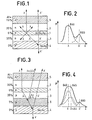
- Figure 1 shows a sectional view of a light emitting diode according to the prior art.
- This is essentially constituted by a layer 1, called active, between two confinement layers 2 and 3, and forming with them, at the two interfaces, two heterojunctions.
- this diode is completed by at least one substrate 4, which serves both as a mechanical support for the thin layers deposited from the substrate, and as the first electrical contact, and in addition by a surface layer 5 said window layer, intended for making a second electrical contact and transparent to the radiation emitted.
- the active layer 1 is made of Al x Ga 1-x As, of p-type doping, comprising 6% of aluminum.
- the two confinement layers 2 and 3 are both made of Al x ' Ga 1-x' As, comprising 35% aluminum, the confinement layer 2 located between the active layer 1 and the emissive surface of the diode being doping. n-type, while the confinement layer 3 located between the active layer 1 and the substrate 4 is p-type doping. Since the substrate 4 is made of p-type GaAs, it therefore contains 0% aluminum. Finally the contact-making layer 5, which constitutes the radiation exit window and the emissive surface of the diode, as opposed to the opaque surface of the substrate 4, is made of Al x " Ga 1x" As, of n-doping type and comprising 15% of aluminum.
- the amount of aluminum contained in a layer regulates the band gap of said layer and therefore imposes the proper emission wavelength of the layer.
- a light emitting diode operating in spontaneous emission regime the radiation of each emissive point is isotropically in space, which is shown in Figure 1 in the form of radiation which, from an element of active layer 1, spreads in all directions in space.
- the confinement layers 2 and 3 and the window layer 5 having aluminum concentrations higher than those of the active layer 1, which comprises only 6% thereof, are transparent to the radiation of this active layer. Consequently, from a volume element of the active layer 1, the radiation of wavelength ⁇ leaves partly through the window layer 5, is partly lost laterally with respect to the structure of the light-emitting diode, and partially strikes the GaAs substrate opaque at this wavelength
- the part of the radiation arriving at the substrate 4 is absorbed by the latter and the loss of energy associated with this absorption allows the reemission by the GaAs substrate, by photoluminescence, at a wavelength specific to the substrate, that is to say ie in the case of example chosen close to 880 nanometers.
- Part of the emission of the substrate, at its own wavelength ⁇ ' passes through the diode without being absorbed either by the active layer or by the confinement layers and therefore exits by the window layer 5 so that, during from the spectral analysis of the electroluminescent component, the wavelength a 'specific to the substrate is taken into account alongside the wavelength X specific to the active layer.
- FIG. 2 represents the optical power of the light-emitting diode, plotted on the ordinate, with respect to the wavelengths plotted on the abscissa. It shows that for a GaAs-AlGaAs type diode, there is a power peak close to 840 nanometers, and a smaller power peak close to 880 nanometers, which corresponds to the power emitted by photoluminescence from the substrate. The envelope of these two peaks gives the spectral analysis of the component.
- the parasitic peak at 880 nanometers can represent up to 40% of the optical power of the main peak at 840 nanometers.
- This spectral duality can compromise the use of the light-emitting diode in a certain number of applications, in particular those in which wavelength multiplexing is used: in these uses, it is necessary that the width of the lines is the most as low as possible and that it be defined as best as possible.
- the parasitic emission phenomenon increases the width of the spectra of the diodes obtained according to the known art: it is therefore necessary to eliminate the parasitic emission.
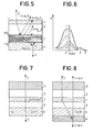
- FIG. 3 represents a sectional view of a light-emitting diode according to the invention, in the case of an opaque substrate.
- the diode according to the invention comprises, placed between the substrate 4 and the confinement layer 3 which is closest to the substrate, an additional layer 6 in Al y Ga 1-y As, of p-type conductivity and containing 5% aluminum.
- the percentage of aluminum in the re-emitting layer 6 must be as close as possible to the percentage of aluminum in the emitting layer 1, but very slightly lower than this, so that the band prohibited from the re-emitting layer is very close to the forbidden band of the emitting layer 1 and in any case less than the forbidden band of the confinement layer 3.
- a volume element of the emitting layer 1 emits light at wavelength ⁇ in the direction of the window layer 5 but also, inter alia, in the direction of the substrate 4: the radiation which is directed towards the substrate is, for a sufficient layer thickness, absorbed by the re-emitting layer 6 and re-emitted by photoluminescence.
- photoluminescent radiation of wavelength ⁇ + ⁇ very close to the wavelength ⁇ of the emitting layer 1 propagates partly towards the window layer 5 and partly towards the substrate .
- the part of this X + A radiation A which is absorbed by the substrate 4 is in turn re-emitted isotropically at the parasitic wavelength ⁇ '.
- FIG. 4 represents the optical power curve of a diode according to the invention, as a function of the wavelength.
- the main optical power peak is slightly widened because it is now made up of the sum of two peaks: the one corresponding to the emission of active layer 1, i.e. in this case the peak at 840 nanometers, and that which corresponds to the re-emission by photoluminescence of the re-emitting layer 6, that is to say in the present case of the order of 845 nanometers.
- the envelope or more exactly the sum of these two energy peaks, makes it possible to obtain a main power peak which is greater than that of the single active layer, at the cost of a slight flattening at the top of the peak since this is very slightly enlarged by the light re-emitted by photoluminescence.
- the presence of the re-emitting layer 6 provides an advantage in that it serves as a smoothing layer on the substrate and that it makes it possible to better adapt the growth of the first GaAI As confinement layer on the GaAs substrate, thus minimizing any stresses, and blocking, during the epitaxy, the migration of defects from the substrate to the layers.
- FIG. 5 represents a sectional view of a light-emitting diode according to the invention, in the case of a variant which still makes it possible to accentuate this advantage. Only the lower part, that is to say the part of the diode between the active layer and the substrate is shown to simplify the figure.
- the re-emitting layer is no longer as in the case of FIG. 3 consisting of a single, layer 6 of homogeneous material, but it is constituted by a set 7 of thinner layers, each layer having an aluminum content, or more generally a band gap, which varies continuously from the substrate towards the active layer 1.
- the first layer in contact with the substrate contains 1% of aluminum, the second layer 2%, and so on until the last layer which comprises 5% of aluminum, if the active layer 1 contains 6 %.
- the radiation emitted by a volume element of the active layer 1, at a wavelength ⁇ , towards the GaAs substrate 4 is absorbed by the last of the layers constituting the re-emitting layer 7, that is to say the layer which is in contact with the confinement layer 3.
- the radiation absorbed in this re-emitting layer is then re-emitted by photoluminescence at a wavelength X ⁇ 1 ⁇ , corresponding to the level of aluminum in said layer.
- the radiation of wavelength ⁇ + ⁇ 1 ⁇ which is itself isotropically emitted in all directions, is in turn absorbed by the next layer and re-emitted at a wavelength X + p 2 X and so on until the first layer, in contact with the substrate, which re-emits at a wavelength ⁇ + ⁇ n X.
- the substrate itself receives a certain radiation which in fact is a mixture of the radiations of the active layer and of the emitting layers 7 but only re-emits a very small part at a parasitic wavelength ⁇ '.
- FIG. 6 shows the energy spectrum of a light-emitting diode according to this first variant of the invention.
- the main energy peak is very slightly widened because it is no longer obtained by the only association of an energy peak corresponding to the active layer 1 and a single energy peak corresponding to the retransmitting layer 6, but it is obtained by association of the energy peak of the emitting layer 1 with a plurality of small energy peaks of the retransmitting sublayers 7.
- the peak d stray energy at 880 nanometers has practically disappeared.
- FIG. 7 represents a sectional view of a light-emitting diode according to the known art, in the second case, according to which the substrate is transparent at the wavelength emitted.
- This type of diode essentially consists of an active layer 1 in Ga x In 1-x As y P 1-y for example, limited by a double heterojunction between two confinement layers 2 and 3 which are both in InP, the together being supported by a substrate 4 in InP also.
- the light emitted by the active layer when it is polarized exits through the window 5, on the upper face of the light-emitting diode, but also exits through the substrate 4 made of InP since it is transparent.
- the wavelength emitted is close to 1,300 nanometers. Between 1,200 and 65,000 nanometers, x and y in the compound Ga x In 1-x As y P 1-y are linked by the relation: with 0.5 ⁇ y ⁇ 1 and 0.22 ⁇ x ⁇ 0.47.
- An emissive diode at 1,300 nanometers, of the kind represented in FIG. 7, can be adapted and receive a structure according to the invention in accordance with the structure exposed in FIG. 3 and its variant of FIG. 5.
- it it is necessary to have between the substrate and the confinement layer 3 - that which is located between the active layer 1 and the substrate 4 - a re-emitting layer which can be either uniform in its thickness and without doping gradient such as layer 6 of the Figure 3, or which may be constituted by a series of thin layers having a doping gradient as shown in 7 in Figure 5.
- the re-emitting layer has a band gap slightly lower than that of the active layer.
- the re-emitting layer 8 In the case where the re-emitting layer 8 is located behind the substrate, the light emitted by a volume element of the active layer passes through the confinement layer 3 and the substrate 4 before being absorbed by the re-emitting layer 8. The latter transforms the absorbed energy and re-emits it in the form of radiation with a wavelength very close to ⁇ + ⁇ , but, since the re-emitting layer is located outside the structure, the radiation re-emitted by photoluminescence is directed in party towards window layer 5, which is one of the objectives originally sought, but also in part towards the rear part of the light-emitting diode.
- the invention has been described on the basis of the two most common cases at present, at 840 and at 1300 nanometers, which also correspond to two interesting cases where the substrate is either opaque or transparent. Nevertheless, the invention applies to all light-emitting diodes, whatever the materials of which it is made, binary or ternary alloy of families III.V. The invention also applies to all light-emitting diodes whatever their structure: in order to simplify the description, the structure of the diodes has been deliberately simplified by removing a certain number of auxiliary layers which have their use but which did not intervene in the description of the invention. The invention also applies to the case of diodes which comprise only one homojunction, or a single heterojunction and not a double heterojunction.
- the general principle of the invention is to replace the part situated on the side of the substrate in a diode, and which either lets light escape through the rear face or absorbs it completely, by what one could compare with a re-emitter, the re-emitting layer, characteristic of the invention, absorbing the light emitted towards the substrate, and re-emitting it towards the window at a wavelength very close to that of the active layer. More generally, the invention is specified by the claims below.
Applications Claiming Priority (2)
| Application Number | Priority Date | Filing Date | Title |
|---|---|---|---|
| FR8221402A FR2538171B1 (fr) | 1982-12-21 | 1982-12-21 | Diode electroluminescente a emission de surface |
| FR8221402 | 1982-12-21 |
Publications (3)
| Publication Number | Publication Date |
|---|---|
| EP0114548A2 true EP0114548A2 (de) | 1984-08-01 |
| EP0114548A3 EP0114548A3 (en) | 1984-12-05 |
| EP0114548B1 EP0114548B1 (de) | 1987-09-30 |
Family
ID=9280328
Family Applications (1)
| Application Number | Title | Priority Date | Filing Date |
|---|---|---|---|
| EP83402409A Expired EP0114548B1 (de) | 1982-12-21 | 1983-12-13 | Elektrolumineszierende Diode mit Oberflächenemission |
Country Status (5)
| Country | Link |
|---|---|
| US (1) | US4570172A (de) |
| EP (1) | EP0114548B1 (de) |
| JP (1) | JPS59121887A (de) |
| DE (1) | DE3373956D1 (de) |
| FR (1) | FR2538171B1 (de) |
Cited By (4)
| Publication number | Priority date | Publication date | Assignee | Title |
|---|---|---|---|---|
| EP0350242A2 (de) * | 1988-07-05 | 1990-01-10 | Hewlett-Packard Company | AlGaAs-Elektrolumineszierende Diode mit doppelten Heteroübergang und mit p-Typ nach oben |
| EP0486052A1 (de) * | 1990-11-16 | 1992-05-20 | Daido Tokushuko Kabushiki Kaisha | Lichtemittierende Diode zur simultanen Ausstrahlung von Lichtern verschiedener Wellenlängen |
| US5260589A (en) * | 1990-11-02 | 1993-11-09 | Norikatsu Yamauchi | Semiconductor device having reflecting layers made of varying unit semiconductors |
| DE19902750A1 (de) * | 1999-01-25 | 2000-08-03 | Osram Opto Semiconductors Gmbh | Halbleiterbauelement zur Erzeugung von mischfarbiger elektromagnetischer Strahlung |
Families Citing this family (30)
| Publication number | Priority date | Publication date | Assignee | Title |
|---|---|---|---|---|
| JPS61166186A (ja) * | 1985-01-18 | 1986-07-26 | Oki Electric Ind Co Ltd | 半導体光素子 |
| US5115286A (en) * | 1988-08-26 | 1992-05-19 | Hewlett-Packard Company | Electro-optical device with inverted transparent substrate and method for making same |
| US5008718A (en) * | 1989-12-18 | 1991-04-16 | Fletcher Robert M | Light-emitting diode with an electrically conductive window |
| JPH0760904B2 (ja) * | 1990-03-19 | 1995-06-28 | イーストマン・コダックジャパン株式会社 | 発光素子 |
| JPH04258182A (ja) * | 1991-02-12 | 1992-09-14 | Mitsubishi Electric Corp | 半導体発光装置 |
| SE468410B (sv) * | 1991-05-08 | 1993-01-11 | Asea Brown Boveri | Ytlysande lysdiod |
| KR940008562B1 (ko) * | 1991-07-20 | 1994-09-24 | 삼성전자 주식회사 | 화합물 반도체 장치 및 그 제조방법 |
| US5481122A (en) * | 1994-07-25 | 1996-01-02 | Industrial Technology Research Institute | Surface light emitting diode with electrically conductive window layer |
| EP1439586B1 (de) * | 1996-06-26 | 2014-03-12 | OSRAM Opto Semiconductors GmbH | Licht abstrahlendes Halbleiterbauelement mit Lumineszenzkonversionselement |
| FR2758888B1 (fr) * | 1997-01-27 | 1999-04-23 | Thomson Csf | Procede de modelisation fine du fouillis de sol recu par un radar |
| US6064076A (en) * | 1998-05-20 | 2000-05-16 | Visual Photonics Epitaxy Co., Ltd. | Light-emitting diode having a transparent substrate |
| TW406442B (en) * | 1998-07-09 | 2000-09-21 | Sumitomo Electric Industries | White colored LED and intermediate colored LED |
| TW413956B (en) * | 1998-07-28 | 2000-12-01 | Sumitomo Electric Industries | Fluorescent substrate LED |
| US6258699B1 (en) | 1999-05-10 | 2001-07-10 | Visual Photonics Epitaxy Co., Ltd. | Light emitting diode with a permanent subtrate of transparent glass or quartz and the method for manufacturing the same |
| US6287882B1 (en) | 1999-10-04 | 2001-09-11 | Visual Photonics Epitaxy Co., Ltd. | Light emitting diode with a metal-coated reflective permanent substrate and the method for manufacturing the same |
| JP4044261B2 (ja) * | 2000-03-10 | 2008-02-06 | 株式会社東芝 | 半導体発光素子及びその製造方法 |
| US6545298B2 (en) * | 2000-10-26 | 2003-04-08 | The Fox Group, Inc. | Compound semiconductor rectifier device structure |
| JP3791765B2 (ja) * | 2001-06-08 | 2006-06-28 | 豊田合成株式会社 | Iii族窒化物系化合物半導体発光素子 |
| US20040227141A1 (en) * | 2003-01-30 | 2004-11-18 | Epistar Corporation | Light emitting device having a high resistivity cushion layer |
| JP4916459B2 (ja) * | 2003-06-05 | 2012-04-11 | パナソニック株式会社 | 半導体発光素子の製造方法 |
| US7402831B2 (en) * | 2004-12-09 | 2008-07-22 | 3M Innovative Properties Company | Adapting short-wavelength LED's for polychromatic, broadband, or “white” emission |
| US7719015B2 (en) * | 2004-12-09 | 2010-05-18 | 3M Innovative Properties Company | Type II broadband or polychromatic LED's |
| US7745814B2 (en) * | 2004-12-09 | 2010-06-29 | 3M Innovative Properties Company | Polychromatic LED's and related semiconductor devices |
| US7335924B2 (en) * | 2005-07-12 | 2008-02-26 | Visual Photonics Epitaxy Co., Ltd. | High-brightness light emitting diode having reflective layer |
| US7384808B2 (en) * | 2005-07-12 | 2008-06-10 | Visual Photonics Epitaxy Co., Ltd. | Fabrication method of high-brightness light emitting diode having reflective layer |
| US7391059B2 (en) | 2005-10-17 | 2008-06-24 | Luminus Devices, Inc. | Isotropic collimation devices and related methods |
| US7388233B2 (en) * | 2005-10-17 | 2008-06-17 | Luminus Devices, Inc. | Patchwork patterned devices and related methods |
| US20070085098A1 (en) * | 2005-10-17 | 2007-04-19 | Luminus Devices, Inc. | Patterned devices and related methods |
| US7348603B2 (en) * | 2005-10-17 | 2008-03-25 | Luminus Devices, Inc. | Anisotropic collimation devices and related methods |
| TWI420693B (zh) * | 2008-07-17 | 2013-12-21 | Advanced Optoelectronic Tech | 發光二極體及其製程 |
Citations (4)
| Publication number | Priority date | Publication date | Assignee | Title |
|---|---|---|---|---|
| US3946417A (en) * | 1972-06-22 | 1976-03-23 | Ibm Corporation | Minimizing cross-talk in L.E.D. arrays |
| FR2390017A1 (de) * | 1977-05-06 | 1978-12-01 | Mitsubishi Monsanto Chem | |
| GB2087145A (en) * | 1980-11-04 | 1982-05-19 | Rca Corp | Light emitting device |
| GB2092370A (en) * | 1981-02-03 | 1982-08-11 | Stanley Electric Co Ltd | An epitaxial wafer of compound semiconductor with light absorbing layer |
Family Cites Families (6)
| Publication number | Priority date | Publication date | Assignee | Title |
|---|---|---|---|---|
| GB1385634A (en) * | 1973-08-21 | 1975-02-26 | Standard Telephones Cables Ltd | Gaa1as lasers |
| DE2737345C2 (de) * | 1976-08-20 | 1991-07-25 | Canon K.K., Tokio/Tokyo | Halbleiterlaser-Vorrichtung mit einem Peltier-Element |
| JPS6038036B2 (ja) * | 1979-04-23 | 1985-08-29 | 松下電器産業株式会社 | 電場発光素子 |
| US4280107A (en) * | 1979-08-08 | 1981-07-21 | Xerox Corporation | Apertured and unapertured reflector structures for electroluminescent devices |
| JPS57109387A (en) * | 1980-12-26 | 1982-07-07 | Fujitsu Ltd | Light emitting element |
| US4438446A (en) * | 1981-05-29 | 1984-03-20 | Bell Telephone Laboratories, Incorporated | Double barrier double heterostructure laser |
-
1982
- 1982-12-21 FR FR8221402A patent/FR2538171B1/fr not_active Expired
-
1983
- 1983-12-13 EP EP83402409A patent/EP0114548B1/de not_active Expired
- 1983-12-13 DE DE8383402409T patent/DE3373956D1/de not_active Expired
- 1983-12-19 US US06/563,247 patent/US4570172A/en not_active Expired - Fee Related
- 1983-12-20 JP JP58240787A patent/JPS59121887A/ja active Pending
Patent Citations (4)
| Publication number | Priority date | Publication date | Assignee | Title |
|---|---|---|---|---|
| US3946417A (en) * | 1972-06-22 | 1976-03-23 | Ibm Corporation | Minimizing cross-talk in L.E.D. arrays |
| FR2390017A1 (de) * | 1977-05-06 | 1978-12-01 | Mitsubishi Monsanto Chem | |
| GB2087145A (en) * | 1980-11-04 | 1982-05-19 | Rca Corp | Light emitting device |
| GB2092370A (en) * | 1981-02-03 | 1982-08-11 | Stanley Electric Co Ltd | An epitaxial wafer of compound semiconductor with light absorbing layer |
Cited By (6)
| Publication number | Priority date | Publication date | Assignee | Title |
|---|---|---|---|---|
| EP0350242A2 (de) * | 1988-07-05 | 1990-01-10 | Hewlett-Packard Company | AlGaAs-Elektrolumineszierende Diode mit doppelten Heteroübergang und mit p-Typ nach oben |
| EP0350242A3 (en) * | 1988-07-05 | 1990-11-22 | Hewlett-Packard Company | P-side up double heterojunction algaas light emitting diode |
| US5260589A (en) * | 1990-11-02 | 1993-11-09 | Norikatsu Yamauchi | Semiconductor device having reflecting layers made of varying unit semiconductors |
| EP0486052A1 (de) * | 1990-11-16 | 1992-05-20 | Daido Tokushuko Kabushiki Kaisha | Lichtemittierende Diode zur simultanen Ausstrahlung von Lichtern verschiedener Wellenlängen |
| DE19902750A1 (de) * | 1999-01-25 | 2000-08-03 | Osram Opto Semiconductors Gmbh | Halbleiterbauelement zur Erzeugung von mischfarbiger elektromagnetischer Strahlung |
| US6900466B2 (en) | 1999-01-25 | 2005-05-31 | Osram Gmbh | Semiconductor component for generating polychromatic electromagnetic radiation |
Also Published As
| Publication number | Publication date |
|---|---|
| FR2538171B1 (fr) | 1986-02-28 |
| JPS59121887A (ja) | 1984-07-14 |
| US4570172A (en) | 1986-02-11 |
| DE3373956D1 (en) | 1987-11-05 |
| EP0114548B1 (de) | 1987-09-30 |
| FR2538171A1 (fr) | 1984-06-22 |
| EP0114548A3 (en) | 1984-12-05 |
Similar Documents
| Publication | Publication Date | Title |
|---|---|---|
| EP0114548B1 (de) | Elektrolumineszierende Diode mit Oberflächenemission | |
| EP1482559B1 (de) | Infrarotdetektor mit unabhängigem, leitfähigem 3D-Gate | |
| EP0869593A1 (de) | Oberflächenemittierender Halbleiterlaser | |
| EP0545808B1 (de) | Optoelektronische Vorrichtung mit sehr niedrigem Serienwiderstand | |
| FR2555370A1 (fr) | Dispositif semi-conducteur servant a engendrer du rayonnement electromagnetique | |
| EP0566494B1 (de) | Elektronenstrahl gepumpter Laserresonator mit asymmetrischer Halbleiter-Heterostruktur | |
| EP3012876B1 (de) | Herstellungsverfahren einer rauscharmen fotodiode | |
| FR2764120A1 (fr) | PHOTODETECTEUR SiGe A RENDEMENT ELEVE | |
| EP0091859A2 (de) | Verfahren zur Herstellung eines Halbleiterlasers mit mehreren unabhängigen Wellenlängen | |
| EP3503222A1 (de) | Verfahren zur herstellung einer optoelektronischen vorrichtung durch aufbringen einer konvertierungsstruktur auf eine emissionsstruktur | |
| EP2504895B1 (de) | Lasersystem, heterostruktur und aktive zone mit gekoppelten sub-quantentöpfen, erzeugung einer laserstrahlung von 1.55 mikrometern | |
| EP0001728A1 (de) | Licht Sende-und Empfangsdiode, insbesondere zur optischen Nachrichtenübertragung | |
| EP0437385B1 (de) | Halbleiterstruktur für optoelektronische Vorrichtung | |
| EP3399559B1 (de) | Leuchtdiode mit wellenlängen-konversionsschichten und deren herstellungsverfahren | |
| EP0082787B1 (de) | Photodiode mit getrennten Absorptions- und Avalanchezonen | |
| EP1169760B1 (de) | Halbleiterlaser für den infraroten wellenlängenbereich | |
| EP0001952B1 (de) | Diode zur Ausstrahlung und zum Empfang von Lichtstrahlen mit derselben bestimmten Wellenlänge | |
| EP0182430A1 (de) | Leuchtdiodenanordnung und ihr Herstellungsverfahren | |
| FR2855654A1 (fr) | Detecteur d'ondes electromagnetiques avec surface de couplage optique comprenant des motifs lamellaires | |
| EP4016762B1 (de) | Laser mit einem verteilten bragg-spiegel und sein herstellungsverfahren | |
| EP0546889B1 (de) | Stromzuführungssystem für eine integrierte Halbleiterlaser-Schaltung | |
| EP4016763B1 (de) | Laser mit einem verteilten bragg-spiegel und sein herstellungsverfahren | |
| FR2485823A1 (fr) | Laser semi-conducteur | |
| FR2721439A1 (fr) | Eléments semi-conducteurs optiques et procédés de fabrication de ceux-ci. | |
| WO2023275320A1 (fr) | Composant optoelectronique insensibles aux dislocations |
Legal Events
| Date | Code | Title | Description |
|---|---|---|---|
| PUAI | Public reference made under article 153(3) epc to a published international application that has entered the european phase |
Free format text: ORIGINAL CODE: 0009012 |
|
| AK | Designated contracting states |
Designated state(s): DE GB NL SE |
|
| PUAL | Search report despatched |
Free format text: ORIGINAL CODE: 0009013 |
|
| AK | Designated contracting states |
Designated state(s): DE GB NL SE |
|
| 17P | Request for examination filed |
Effective date: 19841213 |
|
| 17Q | First examination report despatched |
Effective date: 19860521 |
|
| GRAA | (expected) grant |
Free format text: ORIGINAL CODE: 0009210 |
|
| AK | Designated contracting states |
Kind code of ref document: B1 Designated state(s): DE GB NL SE |
|
| REF | Corresponds to: |
Ref document number: 3373956 Country of ref document: DE Date of ref document: 19871105 |
|
| GBT | Gb: translation of ep patent filed (gb section 77(6)(a)/1977) | ||
| PLBE | No opposition filed within time limit |
Free format text: ORIGINAL CODE: 0009261 |
|
| STAA | Information on the status of an ep patent application or granted ep patent |
Free format text: STATUS: NO OPPOSITION FILED WITHIN TIME LIMIT |
|
| 26N | No opposition filed | ||
| PGFP | Annual fee paid to national office [announced via postgrant information from national office to epo] |
Ref country code: DE Payment date: 19921112 Year of fee payment: 10 |
|
| PGFP | Annual fee paid to national office [announced via postgrant information from national office to epo] |
Ref country code: SE Payment date: 19921113 Year of fee payment: 10 |
|
| PGFP | Annual fee paid to national office [announced via postgrant information from national office to epo] |
Ref country code: GB Payment date: 19921118 Year of fee payment: 10 |
|
| PGFP | Annual fee paid to national office [announced via postgrant information from national office to epo] |
Ref country code: NL Payment date: 19921231 Year of fee payment: 10 |
|
| PG25 | Lapsed in a contracting state [announced via postgrant information from national office to epo] |
Ref country code: GB Effective date: 19931213 |
|
| PG25 | Lapsed in a contracting state [announced via postgrant information from national office to epo] |
Ref country code: SE Effective date: 19931214 |
|
| PG25 | Lapsed in a contracting state [announced via postgrant information from national office to epo] |
Ref country code: NL Effective date: 19940701 |
|
| GBPC | Gb: european patent ceased through non-payment of renewal fee |
Effective date: 19931213 |
|
| NLV4 | Nl: lapsed or anulled due to non-payment of the annual fee | ||
| PG25 | Lapsed in a contracting state [announced via postgrant information from national office to epo] |
Ref country code: DE Effective date: 19940901 |
|
| EUG | Se: european patent has lapsed |
Ref document number: 83402409.3 Effective date: 19940710 |