EP0114548A2 - Electroluminescent diode having a surface emission - Google Patents
Electroluminescent diode having a surface emission Download PDFInfo
- Publication number
- EP0114548A2 EP0114548A2 EP83402409A EP83402409A EP0114548A2 EP 0114548 A2 EP0114548 A2 EP 0114548A2 EP 83402409 A EP83402409 A EP 83402409A EP 83402409 A EP83402409 A EP 83402409A EP 0114548 A2 EP0114548 A2 EP 0114548A2
- Authority
- EP
- European Patent Office
- Prior art keywords
- layer
- substrate
- emitting
- light
- active layer
- Prior art date
- Legal status (The legal status is an assumption and is not a legal conclusion. Google has not performed a legal analysis and makes no representation as to the accuracy of the status listed.)
- Granted
Links
Images
Classifications
-
- H—ELECTRICITY
- H01—ELECTRIC ELEMENTS
- H01L—SEMICONDUCTOR DEVICES NOT COVERED BY CLASS H10
- H01L33/00—Semiconductor devices with at least one potential-jump barrier or surface barrier specially adapted for light emission; Processes or apparatus specially adapted for the manufacture or treatment thereof or of parts thereof; Details thereof
- H01L33/02—Semiconductor devices with at least one potential-jump barrier or surface barrier specially adapted for light emission; Processes or apparatus specially adapted for the manufacture or treatment thereof or of parts thereof; Details thereof characterised by the semiconductor bodies
- H01L33/08—Semiconductor devices with at least one potential-jump barrier or surface barrier specially adapted for light emission; Processes or apparatus specially adapted for the manufacture or treatment thereof or of parts thereof; Details thereof characterised by the semiconductor bodies with a plurality of light emitting regions, e.g. laterally discontinuous light emitting layer or photoluminescent region integrated within the semiconductor body
Definitions
- the present invention relates to a surface emission light emitting diode, the structure of which is adapted to suppress the radiation re-emitted by the substrate.
- a light emitting diode according to the invention comprises a re-emitting layer of a material close to that of the emitting layer, the re-emitting layer absorbing the energy directed towards the substrate to re-emit it at a wavelength close to that of the emitting layer .
- a light-emitting diode is a component essentially formed by an active layer and at least one confinement layer; the whole is carried by a substrate and may further comprise other layers, of smoothing, of contacting, etc., which will not be detailed in the rest of this text, since they do not intervene in the study of the invention.
- a light-emitting diode uses the spontaneous emission resulting from the radiative recombination of electron-hole pairs created by the injection of carriers in a direct polarized junction. Spontaneous radiation is isotropic.
- the optical spectrum associated with the emission comprises one or two more or less distinct peaks depending on the nature of the active layer.
- One of the peaks comes from the substrate which absorbs the energy emitted by the active layer and re-emits it at a wavelength different from that of the active layer.
- the substrate is transparent at the wavelength emitted, it does not re-emit since it does not absorb, but about half of the emitted light is lost: that which comes out from the rear face of the diode, c i.e. through the substrate.
- the invention provides for adding to the structure of the light-emitting diode a layer, placed on the rear path of the emitted light, of a nature very close to that of the active layer, but d band gap energy lower than that of the confinement layers and of the active layer: this additional layer absorbs the radiation emitted at a wavelength X by the active layer, and re-emits it by photoluminescence at a very similar wavelength X + ⁇ .
- the optical power emitted is increased by the photoluminescent emission, and the line width of the optical spectrum is slightly increased, but the parasitic emission peak of the substrate is considerably reduced, or even canceled in certain cases.
- the invention relates to a surface-emitting light-emitting diode, comprising at least one active layer situated between a substrate and a window layer, the active layer emitting, under polarization, an isotropic light radiation of which a part is emitted at through the window layer and a part is emitted in the direction of the substrate, this diode being characterized in that a layer, made of a material whose prohibited band height is close to but less than the prohibited band height of the material of the active layer, absorbs the radiation emitted towards the substrate and re-emits it by photoluminescence, isotropically, at a wavelength ( ⁇ + ⁇ ) very close to the wavelength (X) of the active layer.
- a light-emitting diode can be homojunction, single or double heterojunction, and it can be made of various materials such as those of the families GaAs, AlGaAs, InP, InGaAs, InGaAsP, ... etc.
- GaAs - AlGaAs diode whose GaAs substrate is opaque to radiation, around 840 nanometers, and that a diode whose InP substrate is transparent to radiation, around 1,300 nanometers.
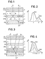
- Figure 1 shows a sectional view of a light emitting diode according to the prior art.
- This is essentially constituted by a layer 1, called active, between two confinement layers 2 and 3, and forming with them, at the two interfaces, two heterojunctions.
- this diode is completed by at least one substrate 4, which serves both as a mechanical support for the thin layers deposited from the substrate, and as the first electrical contact, and in addition by a surface layer 5 said window layer, intended for making a second electrical contact and transparent to the radiation emitted.
- the active layer 1 is made of Al x Ga 1-x As, of p-type doping, comprising 6% of aluminum.
- the two confinement layers 2 and 3 are both made of Al x ' Ga 1-x' As, comprising 35% aluminum, the confinement layer 2 located between the active layer 1 and the emissive surface of the diode being doping. n-type, while the confinement layer 3 located between the active layer 1 and the substrate 4 is p-type doping. Since the substrate 4 is made of p-type GaAs, it therefore contains 0% aluminum. Finally the contact-making layer 5, which constitutes the radiation exit window and the emissive surface of the diode, as opposed to the opaque surface of the substrate 4, is made of Al x " Ga 1x" As, of n-doping type and comprising 15% of aluminum.
- the amount of aluminum contained in a layer regulates the band gap of said layer and therefore imposes the proper emission wavelength of the layer.
- a light emitting diode operating in spontaneous emission regime the radiation of each emissive point is isotropically in space, which is shown in Figure 1 in the form of radiation which, from an element of active layer 1, spreads in all directions in space.
- the confinement layers 2 and 3 and the window layer 5 having aluminum concentrations higher than those of the active layer 1, which comprises only 6% thereof, are transparent to the radiation of this active layer. Consequently, from a volume element of the active layer 1, the radiation of wavelength ⁇ leaves partly through the window layer 5, is partly lost laterally with respect to the structure of the light-emitting diode, and partially strikes the GaAs substrate opaque at this wavelength
- the part of the radiation arriving at the substrate 4 is absorbed by the latter and the loss of energy associated with this absorption allows the reemission by the GaAs substrate, by photoluminescence, at a wavelength specific to the substrate, that is to say ie in the case of example chosen close to 880 nanometers.
- Part of the emission of the substrate, at its own wavelength ⁇ ' passes through the diode without being absorbed either by the active layer or by the confinement layers and therefore exits by the window layer 5 so that, during from the spectral analysis of the electroluminescent component, the wavelength a 'specific to the substrate is taken into account alongside the wavelength X specific to the active layer.
- FIG. 2 represents the optical power of the light-emitting diode, plotted on the ordinate, with respect to the wavelengths plotted on the abscissa. It shows that for a GaAs-AlGaAs type diode, there is a power peak close to 840 nanometers, and a smaller power peak close to 880 nanometers, which corresponds to the power emitted by photoluminescence from the substrate. The envelope of these two peaks gives the spectral analysis of the component.
- the parasitic peak at 880 nanometers can represent up to 40% of the optical power of the main peak at 840 nanometers.
- This spectral duality can compromise the use of the light-emitting diode in a certain number of applications, in particular those in which wavelength multiplexing is used: in these uses, it is necessary that the width of the lines is the most as low as possible and that it be defined as best as possible.
- the parasitic emission phenomenon increases the width of the spectra of the diodes obtained according to the known art: it is therefore necessary to eliminate the parasitic emission.
- FIG. 3 represents a sectional view of a light-emitting diode according to the invention, in the case of an opaque substrate.
- the diode according to the invention comprises, placed between the substrate 4 and the confinement layer 3 which is closest to the substrate, an additional layer 6 in Al y Ga 1-y As, of p-type conductivity and containing 5% aluminum.
- the percentage of aluminum in the re-emitting layer 6 must be as close as possible to the percentage of aluminum in the emitting layer 1, but very slightly lower than this, so that the band prohibited from the re-emitting layer is very close to the forbidden band of the emitting layer 1 and in any case less than the forbidden band of the confinement layer 3.
- a volume element of the emitting layer 1 emits light at wavelength ⁇ in the direction of the window layer 5 but also, inter alia, in the direction of the substrate 4: the radiation which is directed towards the substrate is, for a sufficient layer thickness, absorbed by the re-emitting layer 6 and re-emitted by photoluminescence.
- photoluminescent radiation of wavelength ⁇ + ⁇ very close to the wavelength ⁇ of the emitting layer 1 propagates partly towards the window layer 5 and partly towards the substrate .
- the part of this X + A radiation A which is absorbed by the substrate 4 is in turn re-emitted isotropically at the parasitic wavelength ⁇ '.
- FIG. 4 represents the optical power curve of a diode according to the invention, as a function of the wavelength.
- the main optical power peak is slightly widened because it is now made up of the sum of two peaks: the one corresponding to the emission of active layer 1, i.e. in this case the peak at 840 nanometers, and that which corresponds to the re-emission by photoluminescence of the re-emitting layer 6, that is to say in the present case of the order of 845 nanometers.
- the envelope or more exactly the sum of these two energy peaks, makes it possible to obtain a main power peak which is greater than that of the single active layer, at the cost of a slight flattening at the top of the peak since this is very slightly enlarged by the light re-emitted by photoluminescence.
- the presence of the re-emitting layer 6 provides an advantage in that it serves as a smoothing layer on the substrate and that it makes it possible to better adapt the growth of the first GaAI As confinement layer on the GaAs substrate, thus minimizing any stresses, and blocking, during the epitaxy, the migration of defects from the substrate to the layers.
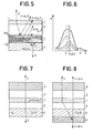
- FIG. 5 represents a sectional view of a light-emitting diode according to the invention, in the case of a variant which still makes it possible to accentuate this advantage. Only the lower part, that is to say the part of the diode between the active layer and the substrate is shown to simplify the figure.
- the re-emitting layer is no longer as in the case of FIG. 3 consisting of a single, layer 6 of homogeneous material, but it is constituted by a set 7 of thinner layers, each layer having an aluminum content, or more generally a band gap, which varies continuously from the substrate towards the active layer 1.
- the first layer in contact with the substrate contains 1% of aluminum, the second layer 2%, and so on until the last layer which comprises 5% of aluminum, if the active layer 1 contains 6 %.
- the radiation emitted by a volume element of the active layer 1, at a wavelength ⁇ , towards the GaAs substrate 4 is absorbed by the last of the layers constituting the re-emitting layer 7, that is to say the layer which is in contact with the confinement layer 3.
- the radiation absorbed in this re-emitting layer is then re-emitted by photoluminescence at a wavelength X ⁇ 1 ⁇ , corresponding to the level of aluminum in said layer.
- the radiation of wavelength ⁇ + ⁇ 1 ⁇ which is itself isotropically emitted in all directions, is in turn absorbed by the next layer and re-emitted at a wavelength X + p 2 X and so on until the first layer, in contact with the substrate, which re-emits at a wavelength ⁇ + ⁇ n X.
- the substrate itself receives a certain radiation which in fact is a mixture of the radiations of the active layer and of the emitting layers 7 but only re-emits a very small part at a parasitic wavelength ⁇ '.
- FIG. 6 shows the energy spectrum of a light-emitting diode according to this first variant of the invention.
- the main energy peak is very slightly widened because it is no longer obtained by the only association of an energy peak corresponding to the active layer 1 and a single energy peak corresponding to the retransmitting layer 6, but it is obtained by association of the energy peak of the emitting layer 1 with a plurality of small energy peaks of the retransmitting sublayers 7.
- the peak d stray energy at 880 nanometers has practically disappeared.
- FIG. 7 represents a sectional view of a light-emitting diode according to the known art, in the second case, according to which the substrate is transparent at the wavelength emitted.
- This type of diode essentially consists of an active layer 1 in Ga x In 1-x As y P 1-y for example, limited by a double heterojunction between two confinement layers 2 and 3 which are both in InP, the together being supported by a substrate 4 in InP also.
- the light emitted by the active layer when it is polarized exits through the window 5, on the upper face of the light-emitting diode, but also exits through the substrate 4 made of InP since it is transparent.
- the wavelength emitted is close to 1,300 nanometers. Between 1,200 and 65,000 nanometers, x and y in the compound Ga x In 1-x As y P 1-y are linked by the relation: with 0.5 ⁇ y ⁇ 1 and 0.22 ⁇ x ⁇ 0.47.
- An emissive diode at 1,300 nanometers, of the kind represented in FIG. 7, can be adapted and receive a structure according to the invention in accordance with the structure exposed in FIG. 3 and its variant of FIG. 5.
- it it is necessary to have between the substrate and the confinement layer 3 - that which is located between the active layer 1 and the substrate 4 - a re-emitting layer which can be either uniform in its thickness and without doping gradient such as layer 6 of the Figure 3, or which may be constituted by a series of thin layers having a doping gradient as shown in 7 in Figure 5.
- the re-emitting layer has a band gap slightly lower than that of the active layer.
- the re-emitting layer 8 In the case where the re-emitting layer 8 is located behind the substrate, the light emitted by a volume element of the active layer passes through the confinement layer 3 and the substrate 4 before being absorbed by the re-emitting layer 8. The latter transforms the absorbed energy and re-emits it in the form of radiation with a wavelength very close to ⁇ + ⁇ , but, since the re-emitting layer is located outside the structure, the radiation re-emitted by photoluminescence is directed in party towards window layer 5, which is one of the objectives originally sought, but also in part towards the rear part of the light-emitting diode.
- the invention has been described on the basis of the two most common cases at present, at 840 and at 1300 nanometers, which also correspond to two interesting cases where the substrate is either opaque or transparent. Nevertheless, the invention applies to all light-emitting diodes, whatever the materials of which it is made, binary or ternary alloy of families III.V. The invention also applies to all light-emitting diodes whatever their structure: in order to simplify the description, the structure of the diodes has been deliberately simplified by removing a certain number of auxiliary layers which have their use but which did not intervene in the description of the invention. The invention also applies to the case of diodes which comprise only one homojunction, or a single heterojunction and not a double heterojunction.
- the general principle of the invention is to replace the part situated on the side of the substrate in a diode, and which either lets light escape through the rear face or absorbs it completely, by what one could compare with a re-emitter, the re-emitting layer, characteristic of the invention, absorbing the light emitted towards the substrate, and re-emitting it towards the window at a wavelength very close to that of the active layer. More generally, the invention is specified by the claims below.
Abstract
L'invention concerne une diode électroluminescente (DEL) dont l'émission lumineuse se fait à travers la surface d'une couche fenêtre. Une DEL comporte au moins une couche active (1) comprise entre un sustrat (4) et une couche fenêtre (5). Sous polarisation, la couche active émet un rayonnement lumineux, de longueur d'onde λ, isotrope. La DEL selon l'invention comporte une couche réémettrice (6) qui absorbe la partie du rayonnement qui est émis en direction du substrat (4) et le réémet, de façon isotrope, avec une longueur d'onde (λ + Δ λ) très proche de celle (λ) de la couche active (1). Pour cela, la couche, réémettrice (6) est en matériau dont la hauteur de bande interdite est très proche mais inférieure à celle de la couche active. Si le substrat (4) est transparent, il peut se trouver entre la couche émettrice (1) et la couche réémettrice (8). Application à l'optoélectronique.The invention relates to a light-emitting diode (LED), the light emission of which is through the surface of a window layer. An LED comprises at least one active layer (1) comprised between a substrate (4) and a window layer (5). Under polarization, the active layer emits light radiation, of wavelength λ, isotropic. The LED according to the invention comprises a re-emitting layer (6) which absorbs the part of the radiation which is emitted in the direction of the substrate (4) and re-emits it, isotropically, with a wavelength (λ + Δ λ) very close to that (λ) of the active layer (1). For this, the re-emitting layer (6) is made of a material whose prohibited band height is very close to but less than that of the active layer. If the substrate (4) is transparent, it may be between the emitting layer (1) and the reemitting layer (8). Application to optoelectronics.
Description
La présente invention concerne une diode électroluminescente à émission de surface, dont la structure est adaptée en vue de supprimer le rayonnement réémis par le substrat. Une diode électroluminescente selon l'invention comporte une couche réémettrice d'un matériau proche de celui de la couche émettrice, la couche réémettrice absorbant l'énergie dirigée vers le substrat pour la réémettre à une longueur d'onde proche de celle de la couche émettrice.The present invention relates to a surface emission light emitting diode, the structure of which is adapted to suppress the radiation re-emitted by the substrate. A light emitting diode according to the invention comprises a re-emitting layer of a material close to that of the emitting layer, the re-emitting layer absorbing the energy directed towards the substrate to re-emit it at a wavelength close to that of the emitting layer .
Une diode électroluminescente est un composant essentiellement formé par une couche active et au moins une couche de confinement ; l'ensemble est porté par un substrat et peut comprendre en outre d'autres couches, de lissage, de prise de contact ... etc., qui ne seront pas détaillées dans la suite de ce texte, car elles n'interviennent pas dans l'étude de l'invention. Une diode électroluminescente utilise l'émission spontanée issue de la recombinaison radiative de paires électron-trou créée par l'injection de porteurs dans une jonction polarisée en direct. Le rayonnement spontané est isotrope.A light-emitting diode is a component essentially formed by an active layer and at least one confinement layer; the whole is carried by a substrate and may further comprise other layers, of smoothing, of contacting, etc., which will not be detailed in the rest of this text, since they do not intervene in the study of the invention. A light-emitting diode uses the spontaneous emission resulting from the radiative recombination of electron-hole pairs created by the injection of carriers in a direct polarized junction. Spontaneous radiation is isotropic.
Deux cas se présentent.Two cases arise.
Dans une diode électroluminescente à émission de surface, dont le substrat est opaque à la longueur d'onde émise, le spectre optique associé à l'émission comporte un ou deux pics plus ou moins distincts suivant la nature de la couche active. L'un des pics provient du substrat qui absorbe l'énergie émise par la couche active et la réémet à une longueur d'onde différente de celle de la couche active.In a surface-emitting light-emitting diode, the substrate of which is opaque to the emitted wavelength, the optical spectrum associated with the emission comprises one or two more or less distinct peaks depending on the nature of the active layer. One of the peaks comes from the substrate which absorbs the energy emitted by the active layer and re-emits it at a wavelength different from that of the active layer.
Si par contre le substrat est transparent à la longueur d'onde émise, il ne réémet pas puisqu'il n'absorbe pas, mais une moitié environ de la lumière émise est perdue : celle qui sort par la face arrière de la diode, c'est-à-dire à travers le substrat.If, on the other hand, the substrate is transparent at the wavelength emitted, it does not re-emit since it does not absorb, but about half of the emitted light is lost: that which comes out from the rear face of the diode, c i.e. through the substrate.
Du fait de la répartition quasi lambertienne du faisceau émis, le rendement d'une diode électroluminescente est assez médiocre, surtout en couplage avec une fibre optique. Afin d'augmenter le rendement d'une diode électroluminescente et d'obtenir un spectre plus pur, l'invention prévoit d'ajouter à la structure de la diode électroluminescente une couche, placée sur le parcours arrière de la lumière émise, de nature très voisine de celle de la couche active, mais d'énergie de bande interdite inférieure à celles des couches de confinement et de la couche active : cette couche supplémentaire absorbe le rayonnement émis à une longueur d'onde X par la couche active, et la réémet par photoluminescence à une longueur d'onde très voisine X + Δλ. Ainsi la puissance optique émise est augmentée par l'émission photoluminescente, et la largeur de raie du spectre optique est légèrement augmentée, mais le pic parasite d'émission du substrat est considérablement diminué, voire annulé dans certains cas. 'Due to the quasi-Lambertian distribution of the emitted beam, the efficiency of a light-emitting diode is quite poor, especially when coupled with an optical fiber. In order to increase the efficiency of a diode to obtain a purer spectrum, the invention provides for adding to the structure of the light-emitting diode a layer, placed on the rear path of the emitted light, of a nature very close to that of the active layer, but d band gap energy lower than that of the confinement layers and of the active layer: this additional layer absorbs the radiation emitted at a wavelength X by the active layer, and re-emits it by photoluminescence at a very similar wavelength X + Δλ. Thus the optical power emitted is increased by the photoluminescent emission, and the line width of the optical spectrum is slightly increased, but the parasitic emission peak of the substrate is considerably reduced, or even canceled in certain cases. ''
De façon plus précise, l'invention concerne une diode électroluminescente à émission de surface, comportant au moins une couche active située entre un substrat et une couche fenêtre, la couche active émettant, sous polarisation, un rayonnement lumineux isotrope dont une partie est émise à travers la couche fenêtre et une partie est émise en direction du substrat, cette diode étant caractérisée en ce qu'une couche, constituée d'un matériau dont la hauteur de bande interdite est voisine mais inférieure à la hauteur de bande interdite du matériau de la couche active, absorbe le rayonnement émis en direction du substrat et le réémet par photoluminescence, de façon isotrope, à une longueur d'onde ( λ+ Δλ) très voisine de la longueur d'onde ( X ) de la couche active.More specifically, the invention relates to a surface-emitting light-emitting diode, comprising at least one active layer situated between a substrate and a window layer, the active layer emitting, under polarization, an isotropic light radiation of which a part is emitted at through the window layer and a part is emitted in the direction of the substrate, this diode being characterized in that a layer, made of a material whose prohibited band height is close to but less than the prohibited band height of the material of the active layer, absorbs the radiation emitted towards the substrate and re-emits it by photoluminescence, isotropically, at a wavelength (λ + Δλ) very close to the wavelength (X) of the active layer.
L'invention sera mieux comprise par la description qui suit de deux exemples de réalisation, concernant les deux cas où le substrat est opaque et où le substrat est transparent à la longueur d'onde émise, cette description s'appuyant sur les figures jointes en annexe et qui représentent :
- - figure 1 : vue en coupe d'une diode électroluminescente selon l'art connu, dans le cas d'un substrat opaque,
- - figure 2 : spectre d'énergie de la diode électroluminescente précédente,
- - figure 3 : vue en coupe d'une diode électroluminescente selon l'invention, dans le cas d'un substrat opaque,
- - figure 4 : spectre d'énergie de la diode électroluminescente de la figure 3,
- - figure 5 : vue en coupe d'une diode électroluminescente selon l'invention dans une première variante,
- - figure 6 : spectre d'énergie de la diode électroluminescente de la figure 5,
- - figure 7 : vue en coupe d'une diode électroluminescente selon l'art :onnu, dans le cas d'un substrat transparent
- - figure 8 : vue en coupe d'une diode électroluminescente selon l'invention dans le cas d'un substrat transparent.
- FIG. 1: sectional view of a light-emitting diode according to the prior art, in the case of an opaque substrate,
- FIG. 2: energy spectrum of the preceding light-emitting diode,
- FIG. 3: sectional view of a light-emitting diode according to the invention, in the case of an opaque substrate,
- FIG. 4: energy spectrum of the light-emitting diode of FIG. 3,
- FIG. 5: sectional view of a light-emitting diode according to the invention in a first variant,
- FIG. 6: energy spectrum of the light-emitting diode of FIG. 5,
- - Figure 7: sectional view of a light emitting diode according to the art: unnu, in the case of a transparent substrate
- - Figure 8: sectional view of a light emitting diode according to the invention in the case of a transparent substrate.
Il existe un grand nombre de types de diodes électroluminescentes, qui varient selon leurs structures ou selon leurs matériaux constitutifs. Une diode électroluminescente peut être à homojonction, à simple ou à double hétérojonction, et elle peut être réalisée en divers matériaux tels que ceux des familles GaAs, AlGaAs, InP, InGaAs, InGaAsP,... etc. Afin d'être plus précis dans l'exposé de l'invention, celle-ci s'appuiera sur deux cas : celui d'une diode GaAs - AlGaAs dont le substrat en GaAs est opaque au rayonnement, voisin de 840 nanomètres, et celui d'une diode dont le substrat en InP est transparent au rayonnement, voisin de 1 300 nanomètres.There are a large number of types of light-emitting diodes, which vary according to their structures or according to their constituent materials. A light-emitting diode can be homojunction, single or double heterojunction, and it can be made of various materials such as those of the families GaAs, AlGaAs, InP, InGaAs, InGaAsP, ... etc. In order to be more precise in the description of the invention, it will be based on two cases: that of a GaAs - AlGaAs diode whose GaAs substrate is opaque to radiation, around 840 nanometers, and that a diode whose InP substrate is transparent to radiation, around 1,300 nanometers.
La figure 1 représente une vue en coupe d'une diode électroluminescente selon l'art connu. Celle-ci est essentiellement constituée par une couche 1, dite active, comprise entre deux couches de confinement 2 et 3, et formant avec elles, aux deux interfaces, deux hétérojonctions. Dans les cas les plus simples, cette diode est complétée par au moins un substrat 4, qui sert à la fois de support mécanique aux fines couches déposées à partir du substrat, et de premier contact électrique, et en outre par une couche de surface 5 dite couche fenêtre, destinée à la prise d'un second contact électrique et transparente au rayonnement émis. La couche active 1 est en AlxGa1-xAs, de dopage de type p, comportant 6 % d'aluminium. Les deux couches de confinement 2 et 3 sont toutes deux en Alx'Ga1-x'As, comportant 35 % d'aluminium, la couche de confinement 2 située entre la couche active 1 et la surface émissive de la diode étant de dopage de type n, tandis que la couche de confinement 3 située entre la couche active 1 et le substrat 4 est de dopage de type p. Le substrat 4 étant en GaAs de type p , il comporte donc 0 % d'aluminium. Enfin la couche 5 de prise de contact, qui constitue la fenêtre de sortie du rayonnement et la surface émissive de la diode, par opposition avec la surface opaque du substrat 4, est en Alx"Ga1x"As, de type de dopage n et comportant 15 % d'aluminium.Figure 1 shows a sectional view of a light emitting diode according to the prior art. This is essentially constituted by a
Le taux d'aluminium contenu dans une couche règle la hauteur de bande interdite de ladite couche et par conséquent impose la longueur d'onde d'émission propre de la couche. Une diode électroluminescente fonctionnant en régime d'émission spontanée, le rayonnement de chaque point émissif s'effectue de manière isotrope dans l'espace, ce qui est représenté sur la figure 1 sous forme d'un rayonnement qui, à partir d'un élément de la couche active 1, se propage dans toutes les directions de l'espace. Les couches de confinement 2 et 3 et la couche fenêtre 5 ayant des concentrations en aluminium supérieures à celles de la couche active 1, qui n'en comporte que 6 %, sont transparentes au rayonnement de cette couche active. Par conséquent, à partir d'un élément de volume de la couche active 1, le rayonnement de longeur d'onde λ sort en partie par la couche fenêtre 5, est en partie perdu latéralement par rapport à la structure de la diode électroluminescente, et vient en partie frapper le substrat en GaAs opaque à cette longueur d'ondeThe amount of aluminum contained in a layer regulates the band gap of said layer and therefore imposes the proper emission wavelength of the layer. A light emitting diode operating in spontaneous emission regime, the radiation of each emissive point is isotropically in space, which is shown in Figure 1 in the form of radiation which, from an element of
La partie du rayonnement arrivant jusqu'au substrat 4 est absorbée par ce dernier et la perte d'énergie associée à cette absorption permet la réémission par le substrat GaAs, par photoluminescence, à une longueur d'onde propre au substrat, c'est-à-dire dans le cas d'exemple choisi voisine de 880 nanomètres. Une partie de l'émission du substrat, à sa longueur d'onde propre λ', traverse la diode sans être absorbée ni par la couche active ni par les couches de confinement et sort donc par la couche fenêtre 5 ce qui fait que, lors de l'analyse spectrale du composant électroluminescent, la longueur d'onde a' propre au substrat est pris en compte à côté de la longueur d'onde X propre à la couche active.The part of the radiation arriving at the
La figure 2 représente la puissance optique de la diode électroluminescente, portée en ordonnées, par rapport aux longueurs d'onde portées en abcisse. Elle met en évidence que pour une diode du type GaAs-AlGaAs, il y a un pic de puissance voisin de 840 nanomètres, et un plus petit pic de puissance voisin de 880 nanomètres, qui correspond à la puissance émise par photoluminescence par le substrat. L'enveloppe de ces deux pics donne l'analyse spectrale du composant. Le pic parasite à 880 nanomètres peut représenter jusque 40 % de la puissance optique du pic principal à 840 nanomètres. Cette dualité spectrale peut compromettre l'utilisation de la diode électroluminescente dans un certain nombre d'applications, en particulier celles dans lesquelles est utilisé le multiplexage en longueur d'onde : dans ces utilisations, il est nécessaire que la largeur des raies soit la plus faible possible et que celle-ci soit définie le mieux possible. Or, en règle générale, le phénomène d'émission parasite augmente la largeur des spectres des diodes obtenues selon l'art connu : il faut donc supprimer l'émission parasite.FIG. 2 represents the optical power of the light-emitting diode, plotted on the ordinate, with respect to the wavelengths plotted on the abscissa. It shows that for a GaAs-AlGaAs type diode, there is a power peak close to 840 nanometers, and a smaller power peak close to 880 nanometers, which corresponds to the power emitted by photoluminescence from the substrate. The envelope of these two peaks gives the spectral analysis of the component. The parasitic peak at 880 nanometers can represent up to 40% of the optical power of the main peak at 840 nanometers. This spectral duality can compromise the use of the light-emitting diode in a certain number of applications, in particular those in which wavelength multiplexing is used: in these uses, it is necessary that the width of the lines is the most as low as possible and that it be defined as best as possible. However, as a general rule, the parasitic emission phenomenon increases the width of the spectra of the diodes obtained according to the known art: it is therefore necessary to eliminate the parasitic emission.
La figure 3 représente une vue en coupe d'une diode électroluminescente selon l'invention, dans le cas d'un substrat opaque. Par rapport à la coupe de diode électroluminescente selon l'art connu de la figure 1, la diode selon l'invention comporte, placée entre le substrat 4 et la couche de confinement 3 qui est la plus proche du substrat, une couche supplémentaire 6 en AlyGa1-yAs, de conductivité de type p et contenant 5 % d'aluminium. De façon plus générale, le pourcentage d'aluminium dans la couche réémettrice 6 doit être le plus proche possible du pourcentage d'aluminium de la couche émettrice 1, mais très légèrement inférieur à celui-ci, de façon à ce que la bande interdite de la couche réémettrice soit très proche de la bande interdite de la couche émettrice 1 et en tout cas inférieur à la bande interdite de la couche de confinement 3.FIG. 3 represents a sectional view of a light-emitting diode according to the invention, in the case of an opaque substrate. Compared to the light-emitting diode section according to the known art of FIG. 1, the diode according to the invention comprises, placed between the
Dans une structure selon l'invention, un élément de volume de la couche émettrice 1 émet de la lumière à longueur d'onde λ en direction de la couche fenêtre 5 mais également, entre autres, en direction du substrat 4 : le rayonnement qui se dirige vers le substrat est, pour une épaisseur de couche suffisante, absorbé par la couche réémettrice 6 et réémis par photoluminescence. Ainsi, à partir de la couche réémettrice 6, un rayonnement photoluminescent de longueur d'onde À + Δλ très proche de la longueur d'onde λ de la couche émettrice 1 se propage en partie vers la couche fenêtre 5 et en partie vers le substrat. La partie de ce rayonnement X + A À qui est absorbée par le substrat 4 est à son tour réémise de façon isotrope à la longueur d'onde parasite λ' .In a structure according to the invention, a volume element of the
La figure 4 représente la courbe de puissance optique d'une diode selon l'invention, en fonction de la longueur d'onde. Par rapport à la courbe de la figure 2, qui représentait la puissance optique d'une diode selon l'art connu, le pic de puissance optique principal est très légèrement élargi car il est désormais constitué par la somme de deux pics : celui qui correspond à l'émission de la couche active 1, c'est-à-dire dans le cas présent le pic à 840 nanomètres, et celui qui correspond à la réémission par photoluminescence de la couche réémettrice 6, c'est-à-dire dans le cas présent de l'ordre de 845 nanomètres. L'enveloppe, ou plus exactement la somme de ces deux pics d'énergie, permet d'obtenir un pic de puissance principal qui est plus important que celui de la seule couche active, au prix d'un léger aplatissement au sommet du pic puisque celui-ci est très légèrement élargi par la lumière réémise par photoluminescence.FIG. 4 represents the optical power curve of a diode according to the invention, as a function of the wavelength. Compared to the curve of FIG. 2, which represented the optical power of a diode according to the known art, the main optical power peak is slightly widened because it is now made up of the sum of two peaks: the one corresponding to the emission of
Par ailleurs, et sur un plan totalement indépendant de la photoluminescence, la présence de la couche réémettrice 6 apporte un avantage en ce sens qu'elle sert de couche de lissage sur le substrat et qu'elle permet de mieux adapter la croissance de la première couche de confinement en GaAI As sur le substrat de GaAs, minimisant ainsi les contraintes éventuelles, et bloquant, au cours de l'épitaxie, la migration des défauts du substrat vers les couches.Furthermore, and on a plane completely independent of photoluminescence, the presence of the
La figure 5 représente une vue en coupe d'une diode électroluminescente selon l'invention, dans le cas d'une variante qui permet encore d'accentuer cet avantage. Seule la partie inférieure, c'est-à-dire la partie de la diode comprise entre la couche active et le substrat est représentée pour simplifier la figure.FIG. 5 represents a sectional view of a light-emitting diode according to the invention, in the case of a variant which still makes it possible to accentuate this advantage. Only the lower part, that is to say the part of the diode between the active layer and the substrate is shown to simplify the figure.
Selon cette variante à l'invention, la couche réémettrice n'est plus comme dans le cas de la figure 3 constituée par une unique ,couche 6 de matériau homogène, mais elle est constituée par un ensemble 7 de couches plus fines, chaque couche ayant une teneur en aluminium, ou de façon plus générale une bande interdite, qui varie de façon continue depuis le substrat en direction de la couche active 1. Pour être plus concret, et toujours dans le cas où le substrat est GaAs opaque à 840 nanomètres, la première couche située au contact du substrat comporte 1 % d'aluminium, la seconde couche 2 %, et ainsi de suite jusqu'à la dernière couche qui comporte 5 % d'aluminium, si la couche active 1 en comporte quant à elle 6 %.According to this variant of the invention, the re-emitting layer is no longer as in the case of FIG. 3 consisting of a single,
Selon cette structure de diode, le rayonnement émis par un élément de volume de la couche active 1, à une longueur d'onde λ , en direction du substrat 4 de GaAs est absorbé par la dernière des couches constituant la couche réémettrice 7, c'est-à-dire la couche qui est en contact avec la couche de confinement 3. Le rayonnement absorbé dans cette couche réémettrice est alors réémis par photoluminescence à une longueur d'onde X Δ1 λ, correspondante au taux d'aluminium dans ladite couche. Le rayonnement de longueur d'onde λ+ Δ1 λ, qui est lui-même émis de façon isotrope dans toutes les directions, est à son tour absorbé par la couche suivante et réémis à une longueur d'onde X + p 2 X et ainsi de suite jusqu'à la première couche, en contact avec le substrat, laquelle réémet à une longueur d'onde λ + Δn X . Le substrat lui-même reçoit un certain rayonnement qui en fait est un mélange des rayonnements de la couche active et des couches émettrices 7 mais ne réémet qu'une très faible partie à une longueur d'onde parasite λ'.According to this diode structure, the radiation emitted by a volume element of the
La figure 6 montre le spectre d'énergie d'une diode électroluminescente selon cette première variante de l'invention. Par comparaison avec le spectre de la figure 4, le pic d'énergie principal est très légèrement élargi du fait qu'il n'est plus obtenu par la seule association d'un pic d'énergie correspondant à la couche active 1 et un seul pic d'énergie correspondant à la couche réémettrice 6, mais qu'il est obtenu par association du pic d'énergie de la couche émettrice 1 avec une pluralité de petits pics d'énergie des sous-couches réémettrices 7. Par contre le pic d'énergie parasite à 880 nanomètres a pratiquement disparu.FIG. 6 shows the energy spectrum of a light-emitting diode according to this first variant of the invention. By comparison with the spectrum of FIG. 4, the main energy peak is very slightly widened because it is no longer obtained by the only association of an energy peak corresponding to the
La figure 7 représente une vue en coupe d'une diode électroluminescente selon l'art connu, dans le second cas, selon lequel le substrat est transparent à la longueur d'onde émise.FIG. 7 represents a sectional view of a light-emitting diode according to the known art, in the second case, according to which the substrate is transparent at the wavelength emitted.
Ce type de diode est essentiellement constitué par une couche active 1 en GaxIn1-xAsyP1-y par exemple, limitée par une double hétérojonction entre deux couches de confinement 2 et 3 qui sont toutes deux en InP, l'ensemble étant supporté par un substrat 4 en InP également. La lumière émise par la couche active lorsqu'elle est polarisée sort à travers la fenêtre 5, sur la face supérieure de la diode électroluminescente, mais sort également à travers le substrat 4 en InP puisque celui-ci est transparent. Dans le cas où la diode est une association entre les couches de InP et de InGaAsP, ou d'autres matériaux voisins, la longueur d'onde émise est voisine de 1 300 nanomètres. Entre 1200 et 65000 nanomètres, x et y dans le composé GaxIn1-x Asy P1-y sont liés par la relation :
Une diode émissive à 1 300 nanomètres, du genre de celle représentée en figure 7, peut être adaptée et recevoir une structure selon l'invention conforme à la structure exposée en figure 3 et à sa variante de la figure 5. Dans ce cas, il faut disposer entre le substrat et la couche de confinement 3 - celle qui se trouve située entre la couche active 1 et le substrat 4 - une couche réémettrice qui peut être soit uniforme dans son épaisseur et sans gradient de dopage telle que la couche 6 de la figure 3, ou qui peut être constituée par une suite de fines couches présentant un gradient de dopage telle que représentée en 7 sur la figure 5. L'important est que la couche réémettrice ait une bande interdite légèrement inférieure à celle de la couche active.An emissive diode at 1,300 nanometers, of the kind represented in FIG. 7, can be adapted and receive a structure according to the invention in accordance with the structure exposed in FIG. 3 and its variant of FIG. 5. In this case, it it is necessary to have between the substrate and the confinement layer 3 - that which is located between the
Cependant, et uniquement dans le cas où le substrat est transparent à ia longueur d'onde émise, un second cas de figure peut être intéressant. C'est celui qui est représenté en figure 8.However, and only in the case where the substrate is transparent to the emitted wavelength, a second scenario can be interesting. This is the one shown in Figure 8.
La différence existant entre la structure de la figure 8 et la structure de la figure 3 est que la couche réémettrice est située, en 8 sur la figure 8 derrière le substrat, vu depuis la couche active, tandis que dans la structure de la figure 3 la couche réémettrice 6 était située devant le substrat, vu depuis la couche émettrice.The difference between the structure of Figure 8 and the structure of Figure 3 is that the re-emitting layer is located, at 8 in Figure 8 behind the substrate, seen from the active layer, while in the structure of Figure 3 the
Dans le cas où la couche réémettrice 8 est située derrière le substrat, la lumière émise par un élément de volume de la couche active traverse la couche de confinement 3 et le substrat 4 avant d'être absorbée par la couche réémettrice 8. Celle-ci transforme l'énergie absorbée et la réémet sous la forme d'un rayonnement de longueur d'onde très voisin λ + Δλ, mais, comme la couche réémettrice est située à l'extérieur de la structure, le rayonnement réémis par photoluminescence est dirigé en partie vers la couche fenêtre 5, ce qui est l'un des objectifs recherché à l'origine, mais également en partie vers la partie arrière de la diode électroluminescente. Le fait qu'un rayonnement sorte par la partie arrière de la diode électroluminescente est, dans certain cas, recherché, afin de pouvoir contrôler la lumière émise par une diode, et assurer par exemple une contre-réaction en fonction de cette lumière émise.In the case where the
L'invention a été décrite en s'appuyant sur les deux cas les plus courants actuellement, à 840 et à 1 300 nanomètres, qui correspondent également à deux cas intéressants où le substrat est soit opaque soit transparent. Néanmoins, l'invention s'applique à toutes diodes électroluminescentes, quels que soient les matériaux dont elle est constituée, alliage binaire ou ternaire des familles III.V. L'invention s'applique également à toutes diodes électroluminescentes quelle que soit leur structure : afin de simplifier l'exposé, la structure des diodes a été volontairement simplifiée en supprimant un certain nombre de couches auxilliaires qui ont leur usage mais qui n'intervenaient pas dans l'exposé de l'invention. L'invention s'applique également au cas de diodes qui ne comportent qu'une homojonction, ou une simple hétérojonction et non pas une double hétérojonction . Le principe général de l'invention est de remplacer la partie située du côté du substrat dans une diode, et qui soit laisse s'échapper de la lumière par la face arrière soit l'absorbe totalement, par ce qu'on pourrait comparer avec un réémetteur, la couche réémettrice, caractéristique de l'invention, absorbant la lumière émise vers le substrat, et la réémettant vers la fenêtre à une longueur d'onde très proche de celle de la couche active. De façon plus générale l'invention est précisée par les revendications ci-après.The invention has been described on the basis of the two most common cases at present, at 840 and at 1300 nanometers, which also correspond to two interesting cases where the substrate is either opaque or transparent. Nevertheless, the invention applies to all light-emitting diodes, whatever the materials of which it is made, binary or ternary alloy of families III.V. The invention also applies to all light-emitting diodes whatever their structure: in order to simplify the description, the structure of the diodes has been deliberately simplified by removing a certain number of auxiliary layers which have their use but which did not intervene in the description of the invention. The invention also applies to the case of diodes which comprise only one homojunction, or a single heterojunction and not a double heterojunction. The general principle of the invention is to replace the part situated on the side of the substrate in a diode, and which either lets light escape through the rear face or absorbs it completely, by what one could compare with a re-emitter, the re-emitting layer, characteristic of the invention, absorbing the light emitted towards the substrate, and re-emitting it towards the window at a wavelength very close to that of the active layer. More generally, the invention is specified by the claims below.
Claims (7)
Applications Claiming Priority (2)
| Application Number | Priority Date | Filing Date | Title |
|---|---|---|---|
| FR8221402 | 1982-12-21 | ||
| FR8221402A FR2538171B1 (en) | 1982-12-21 | 1982-12-21 | SURFACE EMITTING LIGHT EMITTING DIODE |
Publications (3)
| Publication Number | Publication Date |
|---|---|
| EP0114548A2 true EP0114548A2 (en) | 1984-08-01 |
| EP0114548A3 EP0114548A3 (en) | 1984-12-05 |
| EP0114548B1 EP0114548B1 (en) | 1987-09-30 |
Family
ID=9280328
Family Applications (1)
| Application Number | Title | Priority Date | Filing Date |
|---|---|---|---|
| EP83402409A Expired EP0114548B1 (en) | 1982-12-21 | 1983-12-13 | Electroluminescent diode having a surface emission |
Country Status (5)
| Country | Link |
|---|---|
| US (1) | US4570172A (en) |
| EP (1) | EP0114548B1 (en) |
| JP (1) | JPS59121887A (en) |
| DE (1) | DE3373956D1 (en) |
| FR (1) | FR2538171B1 (en) |
Cited By (4)
| Publication number | Priority date | Publication date | Assignee | Title |
|---|---|---|---|---|
| EP0350242A2 (en) * | 1988-07-05 | 1990-01-10 | Hewlett-Packard Company | P-side up double heterojunction AlGaAs light emitting diode |
| EP0486052A1 (en) * | 1990-11-16 | 1992-05-20 | Daido Tokushuko Kabushiki Kaisha | Light-emitting diode for concurrently emitting lights having different wavelengths |
| US5260589A (en) * | 1990-11-02 | 1993-11-09 | Norikatsu Yamauchi | Semiconductor device having reflecting layers made of varying unit semiconductors |
| DE19902750A1 (en) * | 1999-01-25 | 2000-08-03 | Osram Opto Semiconductors Gmbh | Semiconductor component for generating mixed-colored electromagnetic radiation |
Families Citing this family (30)
| Publication number | Priority date | Publication date | Assignee | Title |
|---|---|---|---|---|
| JPS61166186A (en) * | 1985-01-18 | 1986-07-26 | Oki Electric Ind Co Ltd | Semiconductor light element |
| US5115286A (en) * | 1988-08-26 | 1992-05-19 | Hewlett-Packard Company | Electro-optical device with inverted transparent substrate and method for making same |
| US5008718A (en) * | 1989-12-18 | 1991-04-16 | Fletcher Robert M | Light-emitting diode with an electrically conductive window |
| JPH0760904B2 (en) * | 1990-03-19 | 1995-06-28 | イーストマン・コダックジャパン株式会社 | Light emitting element |
| JPH04258182A (en) * | 1991-02-12 | 1992-09-14 | Mitsubishi Electric Corp | Semiconductor light emitting device |
| SE468410B (en) * | 1991-05-08 | 1993-01-11 | Asea Brown Boveri | EXPLANATORY LED |
| KR940008562B1 (en) * | 1991-07-20 | 1994-09-24 | 삼성전자 주식회사 | Compound semiconducator device and manufacturing method thereof |
| US5481122A (en) * | 1994-07-25 | 1996-01-02 | Industrial Technology Research Institute | Surface light emitting diode with electrically conductive window layer |
| JP3773541B2 (en) * | 1996-06-26 | 2006-05-10 | シーメンス アクチエンゲゼルシヤフト | Semiconductor light emitting device having luminescence conversion element |
| FR2758888B1 (en) * | 1997-01-27 | 1999-04-23 | Thomson Csf | PROCESS FOR FINE MODELING OF CLOUD GROUND RECEIVED BY RADAR |
| US6064076A (en) * | 1998-05-20 | 2000-05-16 | Visual Photonics Epitaxy Co., Ltd. | Light-emitting diode having a transparent substrate |
| TW406442B (en) * | 1998-07-09 | 2000-09-21 | Sumitomo Electric Industries | White colored LED and intermediate colored LED |
| TW413956B (en) * | 1998-07-28 | 2000-12-01 | Sumitomo Electric Industries | Fluorescent substrate LED |
| US6258699B1 (en) | 1999-05-10 | 2001-07-10 | Visual Photonics Epitaxy Co., Ltd. | Light emitting diode with a permanent subtrate of transparent glass or quartz and the method for manufacturing the same |
| US6287882B1 (en) | 1999-10-04 | 2001-09-11 | Visual Photonics Epitaxy Co., Ltd. | Light emitting diode with a metal-coated reflective permanent substrate and the method for manufacturing the same |
| JP4044261B2 (en) * | 2000-03-10 | 2008-02-06 | 株式会社東芝 | Semiconductor light emitting device and manufacturing method thereof |
| US6545298B2 (en) * | 2000-10-26 | 2003-04-08 | The Fox Group, Inc. | Compound semiconductor rectifier device structure |
| JP3791765B2 (en) * | 2001-06-08 | 2006-06-28 | 豊田合成株式会社 | Group III nitride compound semiconductor light emitting device |
| US20040227141A1 (en) * | 2003-01-30 | 2004-11-18 | Epistar Corporation | Light emitting device having a high resistivity cushion layer |
| JP4916459B2 (en) * | 2003-06-05 | 2012-04-11 | パナソニック株式会社 | Manufacturing method of semiconductor light emitting device |
| US7402831B2 (en) * | 2004-12-09 | 2008-07-22 | 3M Innovative Properties Company | Adapting short-wavelength LED's for polychromatic, broadband, or “white” emission |
| US7719015B2 (en) * | 2004-12-09 | 2010-05-18 | 3M Innovative Properties Company | Type II broadband or polychromatic LED's |
| US7745814B2 (en) * | 2004-12-09 | 2010-06-29 | 3M Innovative Properties Company | Polychromatic LED's and related semiconductor devices |
| US7384808B2 (en) * | 2005-07-12 | 2008-06-10 | Visual Photonics Epitaxy Co., Ltd. | Fabrication method of high-brightness light emitting diode having reflective layer |
| US7335924B2 (en) * | 2005-07-12 | 2008-02-26 | Visual Photonics Epitaxy Co., Ltd. | High-brightness light emitting diode having reflective layer |
| US7348603B2 (en) * | 2005-10-17 | 2008-03-25 | Luminus Devices, Inc. | Anisotropic collimation devices and related methods |
| US7391059B2 (en) | 2005-10-17 | 2008-06-24 | Luminus Devices, Inc. | Isotropic collimation devices and related methods |
| US20070085098A1 (en) * | 2005-10-17 | 2007-04-19 | Luminus Devices, Inc. | Patterned devices and related methods |
| US7388233B2 (en) * | 2005-10-17 | 2008-06-17 | Luminus Devices, Inc. | Patchwork patterned devices and related methods |
| TWI420693B (en) * | 2008-07-17 | 2013-12-21 | Advanced Optoelectronic Tech | Light emitting device and fabrication thereof |
Citations (4)
| Publication number | Priority date | Publication date | Assignee | Title |
|---|---|---|---|---|
| US3946417A (en) * | 1972-06-22 | 1976-03-23 | Ibm Corporation | Minimizing cross-talk in L.E.D. arrays |
| FR2390017A1 (en) * | 1977-05-06 | 1978-12-01 | Mitsubishi Monsanto Chem | |
| GB2087145A (en) * | 1980-11-04 | 1982-05-19 | Rca Corp | Light emitting device |
| GB2092370A (en) * | 1981-02-03 | 1982-08-11 | Stanley Electric Co Ltd | An epitaxial wafer of compound semiconductor with light absorbing layer |
Family Cites Families (6)
| Publication number | Priority date | Publication date | Assignee | Title |
|---|---|---|---|---|
| GB1385634A (en) * | 1973-08-21 | 1975-02-26 | Standard Telephones Cables Ltd | Gaa1as lasers |
| DE2737345C2 (en) * | 1976-08-20 | 1991-07-25 | Canon K.K., Tokio/Tokyo | Semiconductor laser device with a Peltier element |
| JPS6038036B2 (en) * | 1979-04-23 | 1985-08-29 | 松下電器産業株式会社 | electroluminescent device |
| US4280107A (en) * | 1979-08-08 | 1981-07-21 | Xerox Corporation | Apertured and unapertured reflector structures for electroluminescent devices |
| JPS57109387A (en) * | 1980-12-26 | 1982-07-07 | Fujitsu Ltd | Light emitting element |
| US4438446A (en) * | 1981-05-29 | 1984-03-20 | Bell Telephone Laboratories, Incorporated | Double barrier double heterostructure laser |
-
1982
- 1982-12-21 FR FR8221402A patent/FR2538171B1/en not_active Expired
-
1983
- 1983-12-13 EP EP83402409A patent/EP0114548B1/en not_active Expired
- 1983-12-13 DE DE8383402409T patent/DE3373956D1/en not_active Expired
- 1983-12-19 US US06/563,247 patent/US4570172A/en not_active Expired - Fee Related
- 1983-12-20 JP JP58240787A patent/JPS59121887A/en active Pending
Patent Citations (4)
| Publication number | Priority date | Publication date | Assignee | Title |
|---|---|---|---|---|
| US3946417A (en) * | 1972-06-22 | 1976-03-23 | Ibm Corporation | Minimizing cross-talk in L.E.D. arrays |
| FR2390017A1 (en) * | 1977-05-06 | 1978-12-01 | Mitsubishi Monsanto Chem | |
| GB2087145A (en) * | 1980-11-04 | 1982-05-19 | Rca Corp | Light emitting device |
| GB2092370A (en) * | 1981-02-03 | 1982-08-11 | Stanley Electric Co Ltd | An epitaxial wafer of compound semiconductor with light absorbing layer |
Cited By (6)
| Publication number | Priority date | Publication date | Assignee | Title |
|---|---|---|---|---|
| EP0350242A2 (en) * | 1988-07-05 | 1990-01-10 | Hewlett-Packard Company | P-side up double heterojunction AlGaAs light emitting diode |
| EP0350242A3 (en) * | 1988-07-05 | 1990-11-22 | Hewlett-Packard Company | P-side up double heterojunction algaas light emitting diode |
| US5260589A (en) * | 1990-11-02 | 1993-11-09 | Norikatsu Yamauchi | Semiconductor device having reflecting layers made of varying unit semiconductors |
| EP0486052A1 (en) * | 1990-11-16 | 1992-05-20 | Daido Tokushuko Kabushiki Kaisha | Light-emitting diode for concurrently emitting lights having different wavelengths |
| DE19902750A1 (en) * | 1999-01-25 | 2000-08-03 | Osram Opto Semiconductors Gmbh | Semiconductor component for generating mixed-colored electromagnetic radiation |
| US6900466B2 (en) | 1999-01-25 | 2005-05-31 | Osram Gmbh | Semiconductor component for generating polychromatic electromagnetic radiation |
Also Published As
| Publication number | Publication date |
|---|---|
| US4570172A (en) | 1986-02-11 |
| FR2538171A1 (en) | 1984-06-22 |
| EP0114548B1 (en) | 1987-09-30 |
| EP0114548A3 (en) | 1984-12-05 |
| FR2538171B1 (en) | 1986-02-28 |
| DE3373956D1 (en) | 1987-11-05 |
| JPS59121887A (en) | 1984-07-14 |
Similar Documents
| Publication | Publication Date | Title |
|---|---|---|
| EP0114548B1 (en) | Electroluminescent diode having a surface emission | |
| EP1482559B1 (en) | Infrared detector with independent, conductive, tridimensional gate | |
| EP0869593A1 (en) | Surface emitting semiconductor laser | |
| EP0545808B1 (en) | Optoelectronic device with very low series resistance | |
| FR2555370A1 (en) | SEMICONDUCTOR DEVICE FOR GENERATING ELECTROMAGNETIC RADIATION | |
| EP0566494B1 (en) | Electron beam pumped asymmetric laser cavity with semiconductor heterostructure | |
| EP3012876B1 (en) | Method for manufacturing a low-noise photodiode | |
| FR2764120A1 (en) | HIGH-PERFORMANCE PHOTOGRAPHIC SENSOR | |
| EP0091859A2 (en) | Method for the production of a semiconductor laser having several independent wavelengths | |
| EP3503222A1 (en) | Method for manufacturing an optoelectronic device by transferring a conversion structure onto an emission structure | |
| EP2504895B1 (en) | Laser emission system, heterostructure and active zone comprising coupled sub-quantumwells, use for a laser emiission at 1.55 micrometers | |
| EP0001728A1 (en) | Light emitting and receiving diode, in particular for optical telecommunication | |
| EP0437385B1 (en) | Semiconductor structure for optoelectronic devices | |
| EP3399559B1 (en) | Light-emitting diode comprising wavelength conversion layers and method of manufacturing the same | |
| EP0082787B1 (en) | Photodiode with separated absorption and avalanche regions | |
| EP1169760B1 (en) | Infrared semiconductor laser | |
| EP0001952B1 (en) | Diode emitting and receiving light rays of the same predetermined wavelength | |
| EP0182430A1 (en) | Light-emitting diodes array and method for its production | |
| EP4016762B1 (en) | Laser comprising a distributed bragg reflector and method for manufacturing same | |
| EP0546889B1 (en) | Power supply system for an integrated semiconductor laser circuit | |
| EP4016763B1 (en) | Laser comprising a distributed bragg reflector and method for manufacturing same | |
| FR2485823A1 (en) | SEMICONDUCTOR LASER | |
| FR2721439A1 (en) | Optical semiconductor elements and methods of manufacturing thereof | |
| WO2023275320A1 (en) | Optoelectronic component that is insensitive to dislocations | |
| FR2890491A1 (en) | LIGHT EMITTING DEVICE WITH FILTER LAYER |
Legal Events
| Date | Code | Title | Description |
|---|---|---|---|
| PUAI | Public reference made under article 153(3) epc to a published international application that has entered the european phase |
Free format text: ORIGINAL CODE: 0009012 |
|
| AK | Designated contracting states |
Designated state(s): DE GB NL SE |
|
| PUAL | Search report despatched |
Free format text: ORIGINAL CODE: 0009013 |
|
| AK | Designated contracting states |
Designated state(s): DE GB NL SE |
|
| 17P | Request for examination filed |
Effective date: 19841213 |
|
| 17Q | First examination report despatched |
Effective date: 19860521 |
|
| GRAA | (expected) grant |
Free format text: ORIGINAL CODE: 0009210 |
|
| AK | Designated contracting states |
Kind code of ref document: B1 Designated state(s): DE GB NL SE |
|
| REF | Corresponds to: |
Ref document number: 3373956 Country of ref document: DE Date of ref document: 19871105 |
|
| GBT | Gb: translation of ep patent filed (gb section 77(6)(a)/1977) | ||
| PLBE | No opposition filed within time limit |
Free format text: ORIGINAL CODE: 0009261 |
|
| STAA | Information on the status of an ep patent application or granted ep patent |
Free format text: STATUS: NO OPPOSITION FILED WITHIN TIME LIMIT |
|
| 26N | No opposition filed | ||
| PGFP | Annual fee paid to national office [announced via postgrant information from national office to epo] |
Ref country code: DE Payment date: 19921112 Year of fee payment: 10 |
|
| PGFP | Annual fee paid to national office [announced via postgrant information from national office to epo] |
Ref country code: SE Payment date: 19921113 Year of fee payment: 10 |
|
| PGFP | Annual fee paid to national office [announced via postgrant information from national office to epo] |
Ref country code: GB Payment date: 19921118 Year of fee payment: 10 |
|
| PGFP | Annual fee paid to national office [announced via postgrant information from national office to epo] |
Ref country code: NL Payment date: 19921231 Year of fee payment: 10 |
|
| PG25 | Lapsed in a contracting state [announced via postgrant information from national office to epo] |
Ref country code: GB Effective date: 19931213 |
|
| PG25 | Lapsed in a contracting state [announced via postgrant information from national office to epo] |
Ref country code: SE Effective date: 19931214 |
|
| PG25 | Lapsed in a contracting state [announced via postgrant information from national office to epo] |
Ref country code: NL Effective date: 19940701 |
|
| GBPC | Gb: european patent ceased through non-payment of renewal fee |
Effective date: 19931213 |
|
| NLV4 | Nl: lapsed or anulled due to non-payment of the annual fee | ||
| PG25 | Lapsed in a contracting state [announced via postgrant information from national office to epo] |
Ref country code: DE Effective date: 19940901 |
|
| EUG | Se: european patent has lapsed |
Ref document number: 83402409.3 Effective date: 19940710 |