EP0001952B1 - Diode emitting and receiving light rays of the same predetermined wavelength - Google Patents
Diode emitting and receiving light rays of the same predetermined wavelength Download PDFInfo
- Publication number
- EP0001952B1 EP0001952B1 EP78400155A EP78400155A EP0001952B1 EP 0001952 B1 EP0001952 B1 EP 0001952B1 EP 78400155 A EP78400155 A EP 78400155A EP 78400155 A EP78400155 A EP 78400155A EP 0001952 B1 EP0001952 B1 EP 0001952B1
- Authority
- EP
- European Patent Office
- Prior art keywords
- layer
- diode
- accordance
- layers
- type
- Prior art date
- Legal status (The legal status is an assumption and is not a legal conclusion. Google has not performed a legal analysis and makes no representation as to the accuracy of the status listed.)
- Expired
Links
- 239000000758 substrate Substances 0.000 claims description 8
- 229910045601 alloy Inorganic materials 0.000 claims description 4
- 239000000956 alloy Substances 0.000 claims description 4
- 229910052751 metal Inorganic materials 0.000 claims description 2
- 239000002184 metal Substances 0.000 claims description 2
- 239000004065 semiconductor Substances 0.000 claims description 2
- 230000017525 heat dissipation Effects 0.000 claims 1
- 229910002059 quaternary alloy Inorganic materials 0.000 claims 1
- 229910002058 ternary alloy Inorganic materials 0.000 claims 1
- 230000010287 polarization Effects 0.000 description 5
- 230000005855 radiation Effects 0.000 description 4
- 230000004888 barrier function Effects 0.000 description 3
- JBRZTFJDHDCESZ-UHFFFAOYSA-N AsGa Chemical compound [As]#[Ga] JBRZTFJDHDCESZ-UHFFFAOYSA-N 0.000 description 2
- 229910001218 Gallium arsenide Inorganic materials 0.000 description 2
- 230000005540 biological transmission Effects 0.000 description 2
- 239000000969 carrier Substances 0.000 description 2
- 230000008094 contradictory effect Effects 0.000 description 2
- 239000000203 mixture Substances 0.000 description 2
- 238000005036 potential barrier Methods 0.000 description 2
- 241001080024 Telles Species 0.000 description 1
- 230000003667 anti-reflective effect Effects 0.000 description 1
- 239000012141 concentrate Substances 0.000 description 1
- 239000013078 crystal Substances 0.000 description 1
- 230000008021 deposition Effects 0.000 description 1
- 238000009792 diffusion process Methods 0.000 description 1
- 238000005401 electroluminescence Methods 0.000 description 1
- 239000000835 fiber Substances 0.000 description 1
- 239000000463 material Substances 0.000 description 1
- 239000013307 optical fiber Substances 0.000 description 1
- 230000035945 sensitivity Effects 0.000 description 1
- 239000000126 substance Substances 0.000 description 1
Images


Classifications
-
- H—ELECTRICITY
- H04—ELECTRIC COMMUNICATION TECHNIQUE
- H04B—TRANSMISSION
- H04B10/00—Transmission systems employing electromagnetic waves other than radio-waves, e.g. infrared, visible or ultraviolet light, or employing corpuscular radiation, e.g. quantum communication
- H04B10/40—Transceivers
- H04B10/43—Transceivers using a single component as both light source and receiver, e.g. using a photoemitter as a photoreceiver
-
- H—ELECTRICITY
- H01—ELECTRIC ELEMENTS
- H01L—SEMICONDUCTOR DEVICES NOT COVERED BY CLASS H10
- H01L31/00—Semiconductor devices sensitive to infrared radiation, light, electromagnetic radiation of shorter wavelength or corpuscular radiation and specially adapted either for the conversion of the energy of such radiation into electrical energy or for the control of electrical energy by such radiation; Processes or apparatus specially adapted for the manufacture or treatment thereof or of parts thereof; Details thereof
- H01L31/08—Semiconductor devices sensitive to infrared radiation, light, electromagnetic radiation of shorter wavelength or corpuscular radiation and specially adapted either for the conversion of the energy of such radiation into electrical energy or for the control of electrical energy by such radiation; Processes or apparatus specially adapted for the manufacture or treatment thereof or of parts thereof; Details thereof in which radiation controls flow of current through the device, e.g. photoresistors
- H01L31/10—Semiconductor devices sensitive to infrared radiation, light, electromagnetic radiation of shorter wavelength or corpuscular radiation and specially adapted either for the conversion of the energy of such radiation into electrical energy or for the control of electrical energy by such radiation; Processes or apparatus specially adapted for the manufacture or treatment thereof or of parts thereof; Details thereof in which radiation controls flow of current through the device, e.g. photoresistors characterised by at least one potential-jump barrier or surface barrier, e.g. phototransistors
- H01L31/101—Devices sensitive to infrared, visible or ultraviolet radiation
- H01L31/102—Devices sensitive to infrared, visible or ultraviolet radiation characterised by only one potential barrier or surface barrier
- H01L31/109—Devices sensitive to infrared, visible or ultraviolet radiation characterised by only one potential barrier or surface barrier the potential barrier being of the PN heterojunction type
-
- H—ELECTRICITY
- H01—ELECTRIC ELEMENTS
- H01L—SEMICONDUCTOR DEVICES NOT COVERED BY CLASS H10
- H01L31/00—Semiconductor devices sensitive to infrared radiation, light, electromagnetic radiation of shorter wavelength or corpuscular radiation and specially adapted either for the conversion of the energy of such radiation into electrical energy or for the control of electrical energy by such radiation; Processes or apparatus specially adapted for the manufacture or treatment thereof or of parts thereof; Details thereof
- H01L31/12—Semiconductor devices sensitive to infrared radiation, light, electromagnetic radiation of shorter wavelength or corpuscular radiation and specially adapted either for the conversion of the energy of such radiation into electrical energy or for the control of electrical energy by such radiation; Processes or apparatus specially adapted for the manufacture or treatment thereof or of parts thereof; Details thereof structurally associated with, e.g. formed in or on a common substrate with, one or more electric light sources, e.g. electroluminescent light sources, and electrically or optically coupled thereto
- H01L31/125—Composite devices with photosensitive elements and electroluminescent elements within one single body
-
- H—ELECTRICITY
- H01—ELECTRIC ELEMENTS
- H01L—SEMICONDUCTOR DEVICES NOT COVERED BY CLASS H10
- H01L33/00—Semiconductor devices with at least one potential-jump barrier or surface barrier specially adapted for light emission; Processes or apparatus specially adapted for the manufacture or treatment thereof or of parts thereof; Details thereof
- H01L33/0004—Devices characterised by their operation
- H01L33/002—Devices characterised by their operation having heterojunctions or graded gap
- H01L33/0025—Devices characterised by their operation having heterojunctions or graded gap comprising only AIIIBV compounds
Definitions
- the present invention relates to a diode emitting and receiving light rays of the same predetermined wavelength.
- the emissive zone must have a low thickness so as not to absorb the photons which it generates. It must be heavily doped to have a sufficiently short response time.
- the receiving zone must have a thickness large enough to absorb the photons, and consequently create an electric current and have a weak enough doping to be at least partly in charge of space when the reverse bias voltage is applied.
- these two layers must be prohibited bands of different width.
- the emitting and receiving diode according to the invention is mainly characterized by the superposition of a first emitting layer of a first type of conductivity and of a second receiving layer of a second type of conductivity opposite to the first, the bandwidth the prohibited layer is less than that of the transmitting layer, a third layer of prohibited bandwidth greater than those of the first and second layers being interposed therebetween.
- the substrate and the layer 2 are made of Gallium Arsenide GaAs, the layers 1, 3 and 4 of alloy Ca 1-x , Al x , As.
- Layer 4 has a very large forbidden bandwidth, of the order of 1.8 eV, a thickness of the order of 1 ⁇ m, layer 1, a smaller forbidden bandwidth of the order of 1 , 5 eV, layer 3 with a thickness of around 0.3 ⁇ m has a much larger band gap of 1.8 eV, for example, layer 2 with thickness of the order of 2 ⁇ m at smallest prohibited bandwidth, 1.4 eV and finally the substrate, a prohibited bandwidth of the order of 1.4 eV, and a thickness of 10 to 200 ⁇ m.
- Figure 2 shows when there is no external polarization, the energy levels Ec and Ev of the conduction bands and valence bands of the various regions.
- zone 3 inserted between zones 1 and 2 defines a potential barrier with zone 1.
- the energy levels occupied in the valence bands of regions 1 and 4 correspond to P-type doping.
- the energy levels occupied in the conduction band of zones 3 and 2 correspond to N-type doping. These energy levels being occupied only on either side of the junction, no electric current will not pass.
- zone 1 there are in zone 1, both in the valence and conduction bands, respectively holes and excess electrons. By recombining, these holes and these electrons give rise to the phenomenon of electroluminescence by the creation of photons.
- the holes cannot cross the barrier formed by the valence band in zone 3, and the electrons the barrier formed by the conduction band in zone 4.
- the radiation frequency is proportional to the width of the band prohibited in zone 1.
- the thickness of zone 1, of the order of 1 ⁇ m and its doping of the order of 10 11 at / cm 3 are chosen in an optimal manner, so that the yield in photo- emission and modulation speed of the diode are as high as possible.
- zone 4 is connected to the pole - of a polarization source, the substrate to its pole +. It follows that the potential barriers are accentuated in the vicinity of the junction, and that zones 3 and especially 2 are in charge of space.
- This zone can therefore have a sufficient thickness, 2 ⁇ m for example to absorb the photons, and a weak doping 10 15 at / cm 3 for example, to be easily loaded with space.
- the role of zone 3 is to form the barriers necessary to separate the two functions: transmission and reception. Its thickness 0.3 ⁇ m for example may be small. It is essentially its forbidden bandwidth which must be large and its doping sufficiently low for the space charge to extend in layer 2.
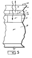
- FIG. 5 represents a diode according to the invention, in which all the types of conductivity are reversed. Furthermore, the design is identical.
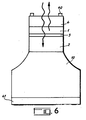
- FIG. 6 represents an exemplary embodiment in the form of a "mesa", the zone 4 exposed to light radiation comprises an annular contact 40.
- the substrate 10 comprises on its free surface a contact 41.
- FIG. 7 Another embodiment is shown in Figure 7.
- the substrate 10 is transparent and its free face is exposed to radiation.
- the arrangement of layers 1, 2, 3 and 4 is reversed compared to the previous figures.
- Layer 2 is welded onto a metal support 42, which serves both as a heat radiator and as a contact: this arrangement promotes the evacuation of heat.
- the diode is of the so-called “mesa diode” welded upside down "type.
- an N-type layer 5, with a small prohibited band, is interposed between zones 2 and 3, it can serve as an avalanche multiplication layer of the electrons generated in layer 2.
- the avalanche phenomenon could occur in layer 3. But in case this doping becomes too high, it can be difficult to put layers 2 and 3 in charge of space.
- the presence of layer 5 in Figure 8 solves this problem.
- the prohibited bandwidth is an increasing function of the value x.
- the layers 1, 2, 3 and 4 will for example have x values respectively of 0.07, for the layer 1, close to 0 for the layer 2, of 0.3 for the layers 3 and 4.
- an anti-reflective treatment that is to say by the deposition on the free surface of the diode (zone 4 or substrate) of a dielectric layer of quarter-wave thickness of known type. , a sensitivity close to 100 A per watt.
- the response time to reception can be short since all carriers are created in the area in charge of space; therefore no natural diffusion process takes place.
- the transit time of the carriers created in the area in charge of space, with a thickness of the order of 2 .mu.m can be less than 100 ps.
- materials other than alloys of the Ga, AI, As type can be used, for example structures based on ternary or quaternary mixtures taken from groups 3 and 5 of the Mendeleef classification.
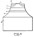
- FIG. 9 represents a structure combining the solutions described in this application and in the French patent application filed on October 18, 1977 under No. 77 31 274 by the applicant and to which the European patent application filed under the number 78400120.8 corresponds. and published under the number 1728.
- annular zone 45 made insulating is provided which makes it possible to concentrate the emission of the current lines in the central part of the diode.
- the invention can also be extended to semiconductor laser structures, FIG. 10.
- the assembly is a single crystal cleaved on two faces.
- Fiber 100 is coupled as shown, layers 2 and 1 receiving and emitting light radiation through the wafer.
Description
La présente invention a pour objet une diode émettrice et réceptrice de rayons lumineux de même longueur d'onde prédetérminée.The present invention relates to a diode emitting and receiving light rays of the same predetermined wavelength.
On sait, que notamment dans le domaine des télécommunications par fibres optiques, on utilise des diodes électroluminescentes ou émettrices, qui, quand elles sont polarisées en direct, émettent des rayons lumineux.. Ces rayons transportent une information. A la réception, une diode polarisée en inverse, délivre un courant électrique qui est fonction de l'intensité des rayons lumineux.It is known that in particular in the field of telecommunications by optical fibers, light-emitting or emitting diodes are used, which, when they are polarized directly, emit light rays. These rays transport information. On reception, a reverse polarized diode delivers an electric current which is a function of the intensity of the light rays.
On a déjà préconisé d'utiliser la même diode pour assurer les deux fonctions en alternat, notamment dans la publication FR-A-2 275 308 de la demande de brevet français 74.20 716 déposée le 14 Juin 1974 par la demanderesse. Ce problème est difficile à résoudre, les qualités exigées dans les deux fonctions étant contradictoires en certains points, si l'on désire des rendements optimaux en émission et en réception.It has already been recommended to use the same diode to perform the two alternating functions, in particular in the publication FR-A-2 275 308 of French patent application 74.20 716 filed on June 14, 1974 by the applicant. This problem is difficult to solve, the qualities required in the two functions being contradictory in certain points, if one wishes optimal yields in transmission and reception.
En effet, la zone émissive doit avoir une épaisseur faible pour ne pas absorber les photons qu'elle engendre. Elle doit être fortement dopée pour avoir un temps de réponse suffisamment faible. Par contre, la zone réceptrice doit avoir une épaisseur assez grande pour absorber les photons, et créer en conséquence un courant électrique et avoir un assez faible dopage pour être au moins en partie en charge d'espace quand la tension de polarisation inverse est appliquée. De plus, ces deux couches doivent être de bandes interdites de largeur différente. Ces conditions, on le voit sont contradictoires. La diode émettrice et réceptrice de lumière selon l'invention permet de résoudre ce problème. La diode émettrice et réceptrice selon l'invention se caractérise principalement par la superposition d'une première couche émettrice d'un premier type de conductivité et d'une deuxième couche réceptrice d'un second type de conductivité opposé au premier, la largeur de bande interdite de la couche réceptrice étant inférieure à celle de la couche émettrice, une troisième couche de largeur de bande interdite supérieure à celles des première et deuxième couches étant interposée entre celles-ci.Indeed, the emissive zone must have a low thickness so as not to absorb the photons which it generates. It must be heavily doped to have a sufficiently short response time. On the other hand, the receiving zone must have a thickness large enough to absorb the photons, and consequently create an electric current and have a weak enough doping to be at least partly in charge of space when the reverse bias voltage is applied. In addition, these two layers must be prohibited bands of different width. These conditions, we see, are contradictory. The light emitting and receiving diode according to the invention solves this problem. The emitting and receiving diode according to the invention is mainly characterized by the superposition of a first emitting layer of a first type of conductivity and of a second receiving layer of a second type of conductivity opposite to the first, the bandwidth the prohibited layer is less than that of the transmitting layer, a third layer of prohibited bandwidth greater than those of the first and second layers being interposed therebetween.
L'invention sera mieux comprise au moyen de la description ci-après en se référant aux dessins annexés parmi lesquels:
- La figure 1 représente très schématiquement un premier exemple de diode selon l'invention.
- La figure 2 représente les niveaux d'énergie au repos dans une telle diode.
- La figure 3 représente les niveaux d'énergie de la même diode en polarisation directe.
- La figure 4 représente les niveaux d'énergie de la même diode en régime de polarisation inverse.
- Les figures 5, 6, 7, 8, 9 et 10 représentent en coupe respectivement des exemples de réalisation de l'invention.
- FIG. 1 very schematically represents a first example of a diode according to the invention.
- FIG. 2 represents the energy levels at rest in such a diode.
- Figure 3 shows the energy levels of the same diode in forward bias.
- FIG. 4 represents the energy levels of the same diode in reverse polarization regime.
- Figures 5, 6, 7, 8, 9 and 10 show in section respectively embodiments of the invention.
Sur la figure 1, sur un substrat 10 de type N+, on a déposé quatre couches de composition chimiques, et par conséquent de largeur de bandes interdites différentes, à savoir dans l'ordre, les couches 2 de type N-, 3 de type N-ou N, 1 de type P+ et 4 de type P+ également. La couche 4 d'épaisseur de l'ordre de 1 ,um est exposée aux rayons lumineux que la diode doit détecter quand elle est polarisée en inverse, et c'est de cette face que sont émis les rayons lumineux, sensiblement de même longueur d'onde, quand elle est polarisée en direct. A titre d'exemple non limitatif, le substrat et la couche 2 sont faits en Arséniure de Gallium GaAs, les couches 1, 3 et 4 d'alliage Ca1-x, Alx, As.In FIG. 1, on an N + type substrate 10, four layers of chemical composition have been deposited, and therefore of different band gap widths, namely in order,
La couche 4 a une largeur de bande interdite très grande, de l'ordre de 1,8 eV, une épaisseur de l'ordre de 1 ,um, la couche 1, une largeur de bande interdite plus faible de l'ordre de 1,5 eV, la couche 3 d'épaisseur de l'ordre de 0,3 µm a une largeur de bande interdite beaucoup plus grande 1,8 eV, par exemple, la couche 2 d'épaifsseurde l'ordre de 2 um a la largeur de bande interdite la plus faible, 1,4 eV et enfin le substrat une largeur de bande interdite de l'ordre de 1,4 eV, et une épaisseur de 10 à 200 µm.
La figure 2 représente quand il n'y a pas de polarisation extérieure, les niveaux d'énergie Ec et Ev des bandes de conduction et des bandes de valence des diverses régions.Figure 2 shows when there is no external polarization, the energy levels Ec and Ev of the conduction bands and valence bands of the various regions.
Sur cette figure, la ligne en traits interrompus Ef représente le niveau de Fermi. On voit clairement que la zone 3 insérée entre les zones 1 et 2 définit une barrière de potentiel avec la zone 1. Les niveaux d'énergie occupés dans les bandes de valence des régions 1 et 4 correspondent à un dopage de type P.In this figure, the dashed line E f represents the Fermi level. We can clearly see that
De même, les niveaux d'energie occupés dans la bande de conduction des zones 3 et 2 correspondent à un dopage de type N. Ces niveaux d'énergie n'étant occupés que de part et d'autre de la jonction, aucun courant électrique ne passera.Similarly, the energy levels occupied in the conduction band of
Sur la figure 3, on a représenté les niveaux d'énergie de la même manière avec une polarisation directe.In FIG. 3, the energy levels are represented in the same way with a direct polarization.
Sur cette figure, on voit clairement qu'il y a dans la zone 1, à la fois dans les bandes de valence et de conduction, respectivement des trous et des électrons en excès. En se recombinant, ces trous et ces électrons donnent naissance au phénomène d'électroluminescence par le création de photons. Les trous ne peuvent franchir la barrière formée par la bande de valence dans la zone 3, et les électrons la barrière formée par la bande de conduction dans la zone 4. La fréquence de rayonnement est proportionnelle à la largeur de la bande interdite dans la zone 1. L'épaisseur de la zone 1, de l'ordre de 1 ,um et son dopage de l'ordre de 1011 at/cm3, sont choisis de façon optimale, pour que le rendement en photo-émission et la vitesse de modulation de la diode soient les plus grandes possible.In this figure, it is clearly seen that there are in
Sur la figure 4, les niveaux d'énergie Ey et Ec sont représentés dans le cas d'une forte polarisation inverse; la zone 4 est reliée au pôle - d'une source de polarisation, le substrat à son pôle +. Il en résulte que les barrières de potentiel sont accentuées au voisinage de la jonction, et que les zones 3 et surtout 2 sont en charge d'espace. Un photon traversant les zones 4, 1 et 3 sans être absorbé en raison de leurs largeurs de bande interdite respectives relativement grandes, est absorbé dans la zone 2 de bande interdite plus faible. Il donne naissance à un trou qui va vers le pôle - et à un électron qui va vers le pôle +. C'est donc la zone 2 qui est essentiellement le siège de la photodétection. Cette zone peut donc avoir une épaisseur suffisante, 2 ,um par exemple pour absorber les photons, et un dopage faible 1015 at/cm3 par exemple, pour être facilement mise en charge d'espace. Le rôle de la zone 3 est de former les barrières nécessaires pour séparer les deux fonctions: émission et réception. Son épaisseur 0,3 µm par exemple peut être faible. C'est essentiellement sa largeur de bande interdite qui doit être grande et son dopage suffisament faible pour que la charge d'espace s'étende dans la couche 2.In FIG. 4, the energy levels E y and E c are represented in the case of a strong reverse polarization;
La figure 5 représente une diode selon l'invention, dans laquelle tous les types de conductivité sont inversés. Par ailleurs, la conception en est identique.FIG. 5 represents a diode according to the invention, in which all the types of conductivity are reversed. Furthermore, the design is identical.
La figure 6 représente un exemple de réalisation en forme de "mésa", la zone 4 exposée au rayonnement lumineux comporte un contact annulaire 40. Le substrat 10 comporte sur sa surface libre un contact 41.FIG. 6 represents an exemplary embodiment in the form of a "mesa", the
Un autre exemple de réalisation est représenté sur la figure 7. Le substrat 10 est transparent et sa face libre est exposée aux radiations. La disposition des couches 1, 2, 3 et 4 est inversée par rapport aux figures précédentes. La couche 2 est soudée sur un support métallique 42, qui sert à la fois de radiateur de chaleur et de contact: cette disposition favorise l'évacuation de la chaleur. La diode est du type dit "diode" mésa "soudée à l'envers".Another embodiment is shown in Figure 7. The
Sur la figure 8, une couche 5 de type N, à petite bande interdite, est interposée entre les zones 2 et 3, elle peut servir de couche de multiplication par avalanche des électrons engendrés dans la couche 2. En dopant plus fortement la couche 3 que la couche 2, le phénomène d'avalanche pourra se produire dans la couche 3. Mais au cas où ce dopage devient trop élevé, il peut être difficile de mettre les couches 2 et 3 en charge d'espace. La présence de la couche 5 de la figure 8 permet de résoudre ce problème.In FIG. 8, an N-type layer 5, with a small prohibited band, is interposed between
Il y a lieu de remarquer que dans le cas d'alliage du type Ga1-x, AIX, As, la largeur de bande interdite est fonction croissante de la valeur x. Dans les exemples décrits plus haut, les couches 1, 2, 3 et 4 auront par exemple des valeurs x respectivement de 0,07, pour la couche 1, voisine de 0 pour la couche 2, de 0,3 pour les couches 3 et 4. On peut espérer, par un traitement antiréfléchissant, c'est-à-dire par le dépôt sur la surface libre de la diode (zone 4 ou substrat) d'une couche diélectrique d'épaisseur quart-d'onde de type connu, une sensibilité voisine de 100 A par watt.It should be noted that in the case of an alloy of the Ga 1-x , AI X , As type, the prohibited bandwidth is an increasing function of the value x. In the examples described above, the
Le temps de réponse à la réception peut être faible puisque tous les porteurs sont crées dans la zone en charge d'espace; donc aucun processus de diffusion naturelle n'intervient. Enfin, le temps de transit des porteurs crées dans la zone en charge d'espace, d'épaisseur de l'ordre de 2 ,um peut être inférieur à 100 ps.The response time to reception can be short since all carriers are created in the area in charge of space; therefore no natural diffusion process takes place. Finally, the transit time of the carriers created in the area in charge of space, with a thickness of the order of 2 .mu.m can be less than 100 ps.
Bien entendu, toutes les valeurs indiquées sont données à titre d'exemple. De plus, d'autres matériaux que les alliages de type Ga, AI, As peuvent être utilisés, par exemple des structures à base de mélanges ternaires ou quaternaires pris dans les groupes 3 et 5 de la classification de Mendeleïef.Of course, all the values indicated are given by way of example. In addition, materials other than alloys of the Ga, AI, As type can be used, for example structures based on ternary or quaternary mixtures taken from
Enfin la figure 9 représente une structure combinant les solutions décrites dans cette demande et dans la demande de brevet français déposée le 18 Octobre 1977 sous le No. 77 31 274 par la demanderesse et à laquelle correspond la demande de brevet européen déposée sous le numéro 78400120.8 et publiée sous le numero 1728. Sur la couche 4, une zone 45 annulaire et rendue isolante est prévue qui permet de concentrer à l'émission les lignes de courant dans la partie centrale de la diode.Finally, FIG. 9 represents a structure combining the solutions described in this application and in the French patent application filed on October 18, 1977 under No. 77 31 274 by the applicant and to which the European patent application filed under the number 78400120.8 corresponds. and published under the number 1728. On
L'invention peut également être étendue à des structures laser semi-conducteur, Fig. 10. Dans ce cas, l'ensemble est un monocristal clivé sur deux faces. La fibre 100 est couplée de la façon indiquée, les couches 2 et 1 recevant et émettant la radiation lumineuse par la tranche.The invention can also be extended to semiconductor laser structures, FIG. 10. In this case, the assembly is a single crystal cleaved on two faces.
Claims (11)
Applications Claiming Priority (2)
| Application Number | Priority Date | Filing Date | Title |
|---|---|---|---|
| FR7733354 | 1977-11-07 | ||
| FR7733354A FR2408222A1 (en) | 1977-11-07 | 1977-11-07 | EMITTING AND RECEIVING DIODE OF LIGHT RAYS OF THE SAME PREDETERMINED WAVELENGTH AND OPTICAL TELECOMMUNICATION DEVICE USING SUCH A DIODE |
Publications (3)
| Publication Number | Publication Date |
|---|---|
| EP0001952A2 EP0001952A2 (en) | 1979-05-16 |
| EP0001952A3 EP0001952A3 (en) | 1979-05-30 |
| EP0001952B1 true EP0001952B1 (en) | 1980-12-10 |
Family
ID=9197316
Family Applications (1)
| Application Number | Title | Priority Date | Filing Date |
|---|---|---|---|
| EP78400155A Expired EP0001952B1 (en) | 1977-11-07 | 1978-10-27 | Diode emitting and receiving light rays of the same predetermined wavelength |
Country Status (6)
| Country | Link |
|---|---|
| US (1) | US4217597A (en) |
| EP (1) | EP0001952B1 (en) |
| JP (1) | JPS5475288A (en) |
| CA (1) | CA1121490A (en) |
| DE (1) | DE2860308D1 (en) |
| FR (1) | FR2408222A1 (en) |
Families Citing this family (4)
| Publication number | Priority date | Publication date | Assignee | Title |
|---|---|---|---|---|
| DE3046140A1 (en) * | 1980-12-06 | 1982-07-15 | Licentia Patent-Verwaltungs-Gmbh, 6000 Frankfurt | "SIGNAL TRANSFER METHOD, A SEMICONDUCTOR COMPONENT AND AN ELECTRO-OPTICAL COMPONENT FOR CARRYING OUT THE PROCESS" |
| EP0096509A3 (en) * | 1982-06-09 | 1986-02-26 | National Research Development Corporation | Electroluminescent devices |
| JPS60230329A (en) * | 1984-04-27 | 1985-11-15 | オプテツクス株式会社 | Infrared ray type photoelectric switch |
| FR2724769B1 (en) * | 1994-09-16 | 1996-12-06 | Thomson Csf | METHOD FOR PRODUCING LASER DIODES WITH SURFACE EMISSION |
Family Cites Families (6)
| Publication number | Priority date | Publication date | Assignee | Title |
|---|---|---|---|---|
| FR2175571B1 (en) * | 1972-03-14 | 1978-08-25 | Radiotechnique Compelec | |
| US3946334A (en) * | 1973-11-14 | 1976-03-23 | Nippon Electric Company, Limited | Injection semiconductor laser device |
| FR2273371B1 (en) * | 1974-05-28 | 1978-03-31 | Thomson Csf | |
| FR2275078A1 (en) * | 1974-06-14 | 1976-01-09 | Thomson Csf | Two-directional optical telecommunication device - comprising, sepd. by fibre optics, diodes which alternately emit and receive light |
| JPS51146196A (en) * | 1975-06-11 | 1976-12-15 | Hitachi Ltd | Diode laser |
| JPS53116792A (en) * | 1977-03-23 | 1978-10-12 | Toshiba Corp | Semiconductor light emitting-photo detecting composite device |
-
1977
- 1977-11-07 FR FR7733354A patent/FR2408222A1/en active Granted
-
1978
- 1978-10-27 DE DE7878400155T patent/DE2860308D1/en not_active Expired
- 1978-10-27 EP EP78400155A patent/EP0001952B1/en not_active Expired
- 1978-10-31 CA CA000315358A patent/CA1121490A/en not_active Expired
- 1978-11-02 US US05/957,196 patent/US4217597A/en not_active Expired - Lifetime
- 1978-11-07 JP JP13720678A patent/JPS5475288A/en active Granted
Also Published As
| Publication number | Publication date |
|---|---|
| JPS6244714B2 (en) | 1987-09-22 |
| EP0001952A2 (en) | 1979-05-16 |
| DE2860308D1 (en) | 1981-02-19 |
| EP0001952A3 (en) | 1979-05-30 |
| CA1121490A (en) | 1982-04-06 |
| US4217597A (en) | 1980-08-12 |
| FR2408222A1 (en) | 1979-06-01 |
| FR2408222B1 (en) | 1980-04-25 |
| JPS5475288A (en) | 1979-06-15 |
Similar Documents
| Publication | Publication Date | Title |
|---|---|---|
| US4202000A (en) | Diode capable of alternately functioning as an emitter and detector of light of the same wavelength | |
| EP0545808B1 (en) | Optoelectronic device with very low series resistance | |
| FR2538171A1 (en) | SURFACE EMITTING ELECTROLUMINESCENT DIODE | |
| EP3084843B1 (en) | Quantum detection element with low noise and method for manufacturing such a photodetection element | |
| EP0001728B1 (en) | Light emitting and receiving diode, in particular for optical telecommunication | |
| JP2004104085A (en) | Avalanche phototransistor | |
| FR2757684A1 (en) | INFRARED DETECTOR WITH QUANTUM STRUCTURE, NOT COOLED | |
| EP0001952B1 (en) | Diode emitting and receiving light rays of the same predetermined wavelength | |
| EP0069608B1 (en) | Short wavelength semiconductor laser | |
| JP4861388B2 (en) | Avalanche photodiode | |
| US5053837A (en) | Ingaas/inp type pin photodiodes | |
| JPS5984589A (en) | Semiconductor photodetector | |
| EP0454566B1 (en) | Electron-pumped compact semiconductor laser | |
| JP2001267620A (en) | Semiconductor photodetector | |
| JPH038117B2 (en) | ||
| US6081020A (en) | Linear PIN photodiode | |
| EP0308335B1 (en) | Ingaas/inp type pin photodiodes | |
| EP0664588A1 (en) | Semiconductor structure with virtual diffraction lattice | |
| CA1182200A (en) | High sensitivity photon feedback photodetectors | |
| EP0082787A2 (en) | Photodiode with separated absorption and avalanche regions | |
| RU2261501C2 (en) | Semiconductor source of infrared radiation | |
| JPH06350134A (en) | Inassb light-emitting diode and its usage method | |
| US20040017600A1 (en) | Electroabsorption modulator, modulator laser device and method for producing an electroabsorption modulator | |
| JPH051629B2 (en) | ||
| FR2485823A1 (en) | SEMICONDUCTOR LASER |
Legal Events
| Date | Code | Title | Description |
|---|---|---|---|
| PUAI | Public reference made under article 153(3) epc to a published international application that has entered the european phase |
Free format text: ORIGINAL CODE: 0009012 |
|
| PUAL | Search report despatched |
Free format text: ORIGINAL CODE: 0009013 |
|
| AK | Designated contracting states |
Designated state(s): DE GB NL |
|
| AK | Designated contracting states |
Designated state(s): DE GB NL |
|
| 17P | Request for examination filed | ||
| GRAA | (expected) grant |
Free format text: ORIGINAL CODE: 0009210 |
|
| AK | Designated contracting states |
Designated state(s): DE GB NL |
|
| REF | Corresponds to: |
Ref document number: 2860308 Country of ref document: DE Date of ref document: 19810219 |
|
| PGFP | Annual fee paid to national office [announced via postgrant information from national office to epo] |
Ref country code: DE Payment date: 19920917 Year of fee payment: 15 |
|
| PGFP | Annual fee paid to national office [announced via postgrant information from national office to epo] |
Ref country code: GB Payment date: 19920918 Year of fee payment: 15 |
|
| PGFP | Annual fee paid to national office [announced via postgrant information from national office to epo] |
Ref country code: NL Payment date: 19921031 Year of fee payment: 15 |
|
| PG25 | Lapsed in a contracting state [announced via postgrant information from national office to epo] |
Ref country code: GB Effective date: 19931027 |
|
| PG25 | Lapsed in a contracting state [announced via postgrant information from national office to epo] |
Ref country code: NL Effective date: 19940501 |
|
| NLV4 | Nl: lapsed or anulled due to non-payment of the annual fee | ||
| GBPC | Gb: european patent ceased through non-payment of renewal fee |
Effective date: 19931027 |
|
| PG25 | Lapsed in a contracting state [announced via postgrant information from national office to epo] |
Ref country code: DE Effective date: 19940802 |
|
| PLBE | No opposition filed within time limit |
Free format text: ORIGINAL CODE: 0009261 |
|
| STAA | Information on the status of an ep patent application or granted ep patent |
Free format text: STATUS: NO OPPOSITION FILED WITHIN TIME LIMIT |