EP0112132A2 - Procédé pour le dépôt d'une couche hautement conductrice et hautement transparente - Google Patents
Procédé pour le dépôt d'une couche hautement conductrice et hautement transparente Download PDFInfo
- Publication number
- EP0112132A2 EP0112132A2 EP83307497A EP83307497A EP0112132A2 EP 0112132 A2 EP0112132 A2 EP 0112132A2 EP 83307497 A EP83307497 A EP 83307497A EP 83307497 A EP83307497 A EP 83307497A EP 0112132 A2 EP0112132 A2 EP 0112132A2
- Authority
- EP
- European Patent Office
- Prior art keywords
- substrate
- onto
- metallic material
- chamber
- metallic
- Prior art date
- Legal status (The legal status is an assumption and is not a legal conclusion. Google has not performed a legal analysis and makes no representation as to the accuracy of the status listed.)
- Granted
Links
- 238000000151 deposition Methods 0.000 title claims abstract description 84
- 238000000034 method Methods 0.000 title claims abstract description 62
- 239000000758 substrate Substances 0.000 claims abstract description 126
- 230000008021 deposition Effects 0.000 claims abstract description 61
- 239000004065 semiconductor Substances 0.000 claims abstract description 34
- 229910044991 metal oxide Inorganic materials 0.000 claims abstract description 30
- 230000008018 melting Effects 0.000 claims abstract description 7
- 238000002844 melting Methods 0.000 claims abstract description 7
- 239000000463 material Substances 0.000 claims description 44
- 239000007769 metal material Substances 0.000 claims description 38
- 150000004706 metal oxides Chemical class 0.000 claims description 25
- 229910052718 tin Inorganic materials 0.000 claims description 18
- ATJFFYVFTNAWJD-UHFFFAOYSA-N Tin Chemical compound [Sn] ATJFFYVFTNAWJD-UHFFFAOYSA-N 0.000 claims description 15
- QVGXLLKOCUKJST-UHFFFAOYSA-N atomic oxygen Chemical compound [O] QVGXLLKOCUKJST-UHFFFAOYSA-N 0.000 claims description 14
- 229910052738 indium Inorganic materials 0.000 claims description 14
- 239000001301 oxygen Substances 0.000 claims description 14
- 238000001704 evaporation Methods 0.000 claims description 13
- 229910052760 oxygen Inorganic materials 0.000 claims description 13
- APFVFJFRJDLVQX-UHFFFAOYSA-N indium atom Chemical compound [In] APFVFJFRJDLVQX-UHFFFAOYSA-N 0.000 claims description 12
- MYMOFIZGZYHOMD-UHFFFAOYSA-N Dioxygen Chemical compound O=O MYMOFIZGZYHOMD-UHFFFAOYSA-N 0.000 claims description 9
- 239000010935 stainless steel Substances 0.000 claims description 9
- 229910001220 stainless steel Inorganic materials 0.000 claims description 9
- 229910001882 dioxygen Inorganic materials 0.000 claims description 8
- 230000008020 evaporation Effects 0.000 claims description 8
- 238000010438 heat treatment Methods 0.000 claims description 8
- HCHKCACWOHOZIP-UHFFFAOYSA-N Zinc Chemical compound [Zn] HCHKCACWOHOZIP-UHFFFAOYSA-N 0.000 claims description 6
- 229910052793 cadmium Inorganic materials 0.000 claims description 6
- 229910052725 zinc Inorganic materials 0.000 claims description 6
- 239000011701 zinc Substances 0.000 claims description 6
- BDOSMKKIYDKNTQ-UHFFFAOYSA-N cadmium atom Chemical compound [Cd] BDOSMKKIYDKNTQ-UHFFFAOYSA-N 0.000 claims description 5
- 239000000203 mixture Substances 0.000 claims description 5
- 239000000088 plastic resin Substances 0.000 claims description 3
- RHZWSUVWRRXEJF-UHFFFAOYSA-N indium tin Chemical compound [In].[Sn] RHZWSUVWRRXEJF-UHFFFAOYSA-N 0.000 claims description 2
- AMGQUBHHOARCQH-UHFFFAOYSA-N indium;oxotin Chemical compound [In].[Sn]=O AMGQUBHHOARCQH-UHFFFAOYSA-N 0.000 claims description 2
- 229910052751 metal Inorganic materials 0.000 abstract description 19
- 239000002184 metal Substances 0.000 abstract description 19
- 239000011521 glass Substances 0.000 abstract description 12
- 238000000576 coating method Methods 0.000 abstract description 10
- 125000004430 oxygen atom Chemical group O* 0.000 abstract description 5
- 238000010923 batch production Methods 0.000 abstract description 3
- 150000002739 metals Chemical class 0.000 abstract description 3
- 238000010924 continuous production Methods 0.000 abstract description 2
- 239000010408 film Substances 0.000 description 53
- 238000004519 manufacturing process Methods 0.000 description 12
- XOLBLPGZBRYERU-UHFFFAOYSA-N tin dioxide Chemical compound O=[Sn]=O XOLBLPGZBRYERU-UHFFFAOYSA-N 0.000 description 11
- 229910045601 alloy Inorganic materials 0.000 description 10
- 239000000956 alloy Substances 0.000 description 10
- PJXISJQVUVHSOJ-UHFFFAOYSA-N indium(III) oxide Inorganic materials [O-2].[O-2].[O-2].[In+3].[In+3] PJXISJQVUVHSOJ-UHFFFAOYSA-N 0.000 description 8
- 229910052787 antimony Inorganic materials 0.000 description 7
- 239000010409 thin film Substances 0.000 description 7
- 125000004429 atom Chemical group 0.000 description 6
- 230000005540 biological transmission Effects 0.000 description 6
- 238000006243 chemical reaction Methods 0.000 description 6
- RYGMFSIKBFXOCR-UHFFFAOYSA-N Copper Chemical compound [Cu] RYGMFSIKBFXOCR-UHFFFAOYSA-N 0.000 description 5
- WATWJIUSRGPENY-UHFFFAOYSA-N antimony atom Chemical compound [Sb] WATWJIUSRGPENY-UHFFFAOYSA-N 0.000 description 5
- 229910052802 copper Inorganic materials 0.000 description 5
- 239000010949 copper Substances 0.000 description 5
- 239000007858 starting material Substances 0.000 description 5
- 239000012799 electrically-conductive coating Substances 0.000 description 4
- 238000004544 sputter deposition Methods 0.000 description 4
- 229910021417 amorphous silicon Inorganic materials 0.000 description 3
- 238000005137 deposition process Methods 0.000 description 3
- 239000002019 doping agent Substances 0.000 description 3
- 230000003287 optical effect Effects 0.000 description 3
- WFKWXMTUELFFGS-UHFFFAOYSA-N tungsten Chemical compound [W] WFKWXMTUELFFGS-UHFFFAOYSA-N 0.000 description 3
- 229910052721 tungsten Inorganic materials 0.000 description 3
- 239000010937 tungsten Substances 0.000 description 3
- XKRFYHLGVUSROY-UHFFFAOYSA-N Argon Chemical compound [Ar] XKRFYHLGVUSROY-UHFFFAOYSA-N 0.000 description 2
- ZOKXTWBITQBERF-UHFFFAOYSA-N Molybdenum Chemical compound [Mo] ZOKXTWBITQBERF-UHFFFAOYSA-N 0.000 description 2
- 229910001128 Sn alloy Inorganic materials 0.000 description 2
- 229910052782 aluminium Inorganic materials 0.000 description 2
- XAGFODPZIPBFFR-UHFFFAOYSA-N aluminium Chemical compound [Al] XAGFODPZIPBFFR-UHFFFAOYSA-N 0.000 description 2
- CXKCTMHTOKXKQT-UHFFFAOYSA-N cadmium oxide Chemical compound [Cd]=O CXKCTMHTOKXKQT-UHFFFAOYSA-N 0.000 description 2
- 239000011248 coating agent Substances 0.000 description 2
- 230000001747 exhibiting effect Effects 0.000 description 2
- 239000007789 gas Substances 0.000 description 2
- 229910003437 indium oxide Inorganic materials 0.000 description 2
- 239000011261 inert gas Substances 0.000 description 2
- 229910052750 molybdenum Inorganic materials 0.000 description 2
- 239000011733 molybdenum Substances 0.000 description 2
- 230000007935 neutral effect Effects 0.000 description 2
- 239000007787 solid Substances 0.000 description 2
- 229910001887 tin oxide Inorganic materials 0.000 description 2
- VYZAMTAEIAYCRO-UHFFFAOYSA-N Chromium Chemical compound [Cr] VYZAMTAEIAYCRO-UHFFFAOYSA-N 0.000 description 1
- YCKRFDGAMUMZLT-UHFFFAOYSA-N Fluorine atom Chemical compound [F] YCKRFDGAMUMZLT-UHFFFAOYSA-N 0.000 description 1
- 229910000846 In alloy Inorganic materials 0.000 description 1
- 229910000979 O alloy Inorganic materials 0.000 description 1
- 229910000676 Si alloy Inorganic materials 0.000 description 1
- XUIMIQQOPSSXEZ-UHFFFAOYSA-N Silicon Chemical compound [Si] XUIMIQQOPSSXEZ-UHFFFAOYSA-N 0.000 description 1
- 238000010521 absorption reaction Methods 0.000 description 1
- 238000005275 alloying Methods 0.000 description 1
- GVFOJDIFWSDNOY-UHFFFAOYSA-N antimony tin Chemical class [Sn].[Sb] GVFOJDIFWSDNOY-UHFFFAOYSA-N 0.000 description 1
- 229910052786 argon Inorganic materials 0.000 description 1
- 229910052797 bismuth Inorganic materials 0.000 description 1
- JCXGWMGPZLAOME-UHFFFAOYSA-N bismuth atom Chemical compound [Bi] JCXGWMGPZLAOME-UHFFFAOYSA-N 0.000 description 1
- 239000000919 ceramic Substances 0.000 description 1
- 229910010293 ceramic material Inorganic materials 0.000 description 1
- 238000005229 chemical vapour deposition Methods 0.000 description 1
- 238000010276 construction Methods 0.000 description 1
- 239000013078 crystal Substances 0.000 description 1
- 229910021419 crystalline silicon Inorganic materials 0.000 description 1
- 238000002425 crystallisation Methods 0.000 description 1
- 230000008025 crystallization Effects 0.000 description 1
- 230000007423 decrease Effects 0.000 description 1
- 230000007547 defect Effects 0.000 description 1
- 230000001419 dependent effect Effects 0.000 description 1
- 230000000694 effects Effects 0.000 description 1
- 238000010894 electron beam technology Methods 0.000 description 1
- 239000011737 fluorine Substances 0.000 description 1
- 229910052731 fluorine Inorganic materials 0.000 description 1
- 229910052732 germanium Inorganic materials 0.000 description 1
- GNPVGFCGXDBREM-UHFFFAOYSA-N germanium atom Chemical compound [Ge] GNPVGFCGXDBREM-UHFFFAOYSA-N 0.000 description 1
- 150000004820 halides Chemical class 0.000 description 1
- 239000012535 impurity Substances 0.000 description 1
- 239000011810 insulating material Substances 0.000 description 1
- 238000002955 isolation Methods 0.000 description 1
- 239000004973 liquid crystal related substance Substances 0.000 description 1
- 229910001507 metal halide Inorganic materials 0.000 description 1
- 150000005309 metal halides Chemical class 0.000 description 1
- 230000004048 modification Effects 0.000 description 1
- 238000012986 modification Methods 0.000 description 1
- 229910000510 noble metal Inorganic materials 0.000 description 1
- 239000000615 nonconductor Substances 0.000 description 1
- 125000002524 organometallic group Chemical group 0.000 description 1
- 230000003647 oxidation Effects 0.000 description 1
- 238000007254 oxidation reaction Methods 0.000 description 1
- 229920000728 polyester Polymers 0.000 description 1
- 238000002360 preparation method Methods 0.000 description 1
- 238000005086 pumping Methods 0.000 description 1
- 239000010453 quartz Substances 0.000 description 1
- 238000010791 quenching Methods 0.000 description 1
- 230000000171 quenching effect Effects 0.000 description 1
- 239000011347 resin Substances 0.000 description 1
- 229920005989 resin Polymers 0.000 description 1
- 230000000284 resting effect Effects 0.000 description 1
- 229910052710 silicon Inorganic materials 0.000 description 1
- 239000010703 silicon Substances 0.000 description 1
- VYPSYNLAJGMNEJ-UHFFFAOYSA-N silicon dioxide Inorganic materials O=[Si]=O VYPSYNLAJGMNEJ-UHFFFAOYSA-N 0.000 description 1
- 238000001228 spectrum Methods 0.000 description 1
- 229940071182 stannate Drugs 0.000 description 1
- 238000003860 storage Methods 0.000 description 1
- 239000000126 substance Substances 0.000 description 1
- 230000002194 synthesizing effect Effects 0.000 description 1
- 229910052715 tantalum Inorganic materials 0.000 description 1
- GUVRBAGPIYLISA-UHFFFAOYSA-N tantalum atom Chemical compound [Ta] GUVRBAGPIYLISA-UHFFFAOYSA-N 0.000 description 1
- 238000007740 vapor deposition Methods 0.000 description 1
Images

Classifications
-
- H—ELECTRICITY
- H01—ELECTRIC ELEMENTS
- H01L—SEMICONDUCTOR DEVICES NOT COVERED BY CLASS H10
- H01L31/00—Semiconductor devices sensitive to infrared radiation, light, electromagnetic radiation of shorter wavelength or corpuscular radiation and specially adapted either for the conversion of the energy of such radiation into electrical energy or for the control of electrical energy by such radiation; Processes or apparatus specially adapted for the manufacture or treatment thereof or of parts thereof; Details thereof
- H01L31/18—Processes or apparatus specially adapted for the manufacture or treatment of these devices or of parts thereof
- H01L31/1884—Manufacture of transparent electrodes, e.g. TCO, ITO
-
- H—ELECTRICITY
- H01—ELECTRIC ELEMENTS
- H01L—SEMICONDUCTOR DEVICES NOT COVERED BY CLASS H10
- H01L31/00—Semiconductor devices sensitive to infrared radiation, light, electromagnetic radiation of shorter wavelength or corpuscular radiation and specially adapted either for the conversion of the energy of such radiation into electrical energy or for the control of electrical energy by such radiation; Processes or apparatus specially adapted for the manufacture or treatment thereof or of parts thereof; Details thereof
-
- C—CHEMISTRY; METALLURGY
- C23—COATING METALLIC MATERIAL; COATING MATERIAL WITH METALLIC MATERIAL; CHEMICAL SURFACE TREATMENT; DIFFUSION TREATMENT OF METALLIC MATERIAL; COATING BY VACUUM EVAPORATION, BY SPUTTERING, BY ION IMPLANTATION OR BY CHEMICAL VAPOUR DEPOSITION, IN GENERAL; INHIBITING CORROSION OF METALLIC MATERIAL OR INCRUSTATION IN GENERAL
- C23C—COATING METALLIC MATERIAL; COATING MATERIAL WITH METALLIC MATERIAL; SURFACE TREATMENT OF METALLIC MATERIAL BY DIFFUSION INTO THE SURFACE, BY CHEMICAL CONVERSION OR SUBSTITUTION; COATING BY VACUUM EVAPORATION, BY SPUTTERING, BY ION IMPLANTATION OR BY CHEMICAL VAPOUR DEPOSITION, IN GENERAL
- C23C14/00—Coating by vacuum evaporation, by sputtering or by ion implantation of the coating forming material
- C23C14/06—Coating by vacuum evaporation, by sputtering or by ion implantation of the coating forming material characterised by the coating material
- C23C14/08—Oxides
- C23C14/086—Oxides of zinc, germanium, cadmium, indium, tin, thallium or bismuth
-
- H—ELECTRICITY
- H01—ELECTRIC ELEMENTS
- H01L—SEMICONDUCTOR DEVICES NOT COVERED BY CLASS H10
- H01L31/00—Semiconductor devices sensitive to infrared radiation, light, electromagnetic radiation of shorter wavelength or corpuscular radiation and specially adapted either for the conversion of the energy of such radiation into electrical energy or for the control of electrical energy by such radiation; Processes or apparatus specially adapted for the manufacture or treatment thereof or of parts thereof; Details thereof
- H01L31/18—Processes or apparatus specially adapted for the manufacture or treatment of these devices or of parts thereof
- H01L31/20—Processes or apparatus specially adapted for the manufacture or treatment of these devices or of parts thereof such devices or parts thereof comprising amorphous semiconductor materials
- H01L31/206—Particular processes or apparatus for continuous treatment of the devices, e.g. roll-to roll processes, multi-chamber deposition
-
- Y—GENERAL TAGGING OF NEW TECHNOLOGICAL DEVELOPMENTS; GENERAL TAGGING OF CROSS-SECTIONAL TECHNOLOGIES SPANNING OVER SEVERAL SECTIONS OF THE IPC; TECHNICAL SUBJECTS COVERED BY FORMER USPC CROSS-REFERENCE ART COLLECTIONS [XRACs] AND DIGESTS
- Y02—TECHNOLOGIES OR APPLICATIONS FOR MITIGATION OR ADAPTATION AGAINST CLIMATE CHANGE
- Y02E—REDUCTION OF GREENHOUSE GAS [GHG] EMISSIONS, RELATED TO ENERGY GENERATION, TRANSMISSION OR DISTRIBUTION
- Y02E10/00—Energy generation through renewable energy sources
- Y02E10/50—Photovoltaic [PV] energy
-
- Y—GENERAL TAGGING OF NEW TECHNOLOGICAL DEVELOPMENTS; GENERAL TAGGING OF CROSS-SECTIONAL TECHNOLOGIES SPANNING OVER SEVERAL SECTIONS OF THE IPC; TECHNICAL SUBJECTS COVERED BY FORMER USPC CROSS-REFERENCE ART COLLECTIONS [XRACs] AND DIGESTS
- Y02—TECHNOLOGIES OR APPLICATIONS FOR MITIGATION OR ADAPTATION AGAINST CLIMATE CHANGE
- Y02P—CLIMATE CHANGE MITIGATION TECHNOLOGIES IN THE PRODUCTION OR PROCESSING OF GOODS
- Y02P70/00—Climate change mitigation technologies in the production process for final industrial or consumer products
- Y02P70/50—Manufacturing or production processes characterised by the final manufactured product
Definitions
- the present invention relates generally to methods of and apparatus for depositing thin, highly light transmissive, highly electrically conductive films, and more particularly, to processes and apparatus for efficiently depositing such a film onto a substrate as a step in the production of semiconductor devices.
- This invention in one preferred embodiment, relates to an improved method of and apparatus for depositing a thin, highly electrically conductive, highly light transmissive, low melting point metal oxide film onto the surface of an amorphous semiconductor material to manufacture a photovoltaic device.
- the multiple cell structures therein discussed utilized p-n junction crystalline semiconductor devices. Essentially the concept is directed to utilizing different band gap devices to more efficiently collect various portions of the solar spectrum and to increase open circuit voltage (Voc).
- the tandem cell device has two or more cells with the light directed serially through each cell, with a large band gap material followed by one or more smaller band gap materials to absorb the light passed through the proceeding cell or layer.
- amorphous silicon alloys can now be deposited in multiple layers over large area. substrates to form solar cells in a high volume, continuous processing system.
- Continuous processing systems of this kind are disclosed, for example, in pending patent applications: Serial No. 151,301, (Pat. no. 4400409) for A Method Of Making P-Doped Silicon Films and Devices Made Therefrom; Serial No. 244,386, filed March 16, 1981 for Continuous Systems For Depositing Amorphous Semiconductor Material: Serial No. 240,493, filed March 16, 1981 for Continuous Amorphous Solar Cell Production System; EPA no.82Z08699.8 filed September.
- a substrate formed from stainless steel may be continuously advanced through a succession of deposition chambers, wherein each chamber is dedicated , to the deposition of a specific material.
- a further deposition process may. be performed either in a separate environment or as a part of a continuous process.
- a thin, transparent or semitransparent film of electrically-conductive, light transmissive material such as TCO (transparent conductive oxide) of, for example, an alloy of indium, tin, and oxygen (ITO) is added.
- TCO transparent conductive oxide
- ITO indium, tin, and oxygen
- Such thin, electrically-conductive films which are also highly light transmissive in the visible range, has a variety of other important optical and electrical applications.
- These films may be used, inter alia, as: antistatic coatings; electrodes in photoconductor storage devices; liquid crystal and electrochromic displays; photothermal absorption devices; and active and passive layers in photovoltaic devices.
- thin transparent, conductive metal oxide coatings used for the purposes outlined hereinabove, commonly comprise: tin oxide materials such as Sn0 2 and Sn0 2 doped with antimony or other elements; In 2 O 3 and In 2 O 3 doped with tin or other elements; or cadmium oxygen materials such as CdO and cadmium oxygen doped with tin.
- tin oxide materials such as Sn0 2 and Sn0 2 doped with antimony or other elements
- In 2 O 3 and In 2 O 3 doped with tin or other elements or cadmium oxygen materials such as CdO and cadmium oxygen doped with tin.
- such materials as IN 2 O 31 SnO 2 and ZnO are regarded as electrical insulators unless combined with a dopant, and formed in a manner which develops a large number of oxygen vacancies.
- tin is commonly used to dope indium oxide
- other metals such as cadmium, bismuth and molybdenum may also be
- a first production technique is a variant of a sputtering process in which d.c. or r.f. signals bombard metal-oxide targets and, thereby, eject the metal-oxide material of the targets for deposition onto a substrate.
- d.c. or r.f. sputtering signals are used with metal targets. This is accompaied by a post-ejection reaction in oxygen to create the material for deposition, the reaction occuring in a plasma generated by the sputtering signal.
- the foregoing processes involve high electrical and kinetic energies, relatively slow rates of deposition, and require post-deposition heating.
- an inert gas such as argon be introduced within the plasma zone to aid in the ionization of the oxygen atoms
- a magnetic field be employed to move the electrons through the zone in a helical path for increasing the length of time the electrons remain in the zone, thereby increasing the number of possible electron collisions with oxygen and metal atoms.
- the deposition of ultra-thin noble metals by evaporation or sputtering processes can provide a film exhibiting excellent electrical properties, the film lacks the requisite light transmissivity in the visible range;
- the deposition of thin films by said fabrication processes may additionally require post-deposition oxidation by heating in oxygen;
- the deposition of thin films by processes such as chemical vapor deposition, (deposition from a heated chemical vapor which typically includes a metal halide and H 2 0 vapor) requires elevated temperatures and includes the inherent, corrosive effects of halides, -high stresses in the deposited film and impurities from the deposition atmosphere; and (4) the deposition of thin films comprising organometallics is costly.
- the improved method of and apparatus for depositing thin, light transmissive, electrically-conductive coatings onto the surface of a substrate employs r.f. power to form the plasma from process gases introduced into a deposition chamber.
- the r.f. signal is particularly advantageous because the high frequency increases the number of metal atom-oxygen atom collisions necessary to generate an ionized plasma and the collision occurs at lower pressure than was possible with the methods and apparatus discussed supra.
- the deposition process and apparatus described herein provides highly electrically conductive films which are highly transmissive in the visible range, formed of In 2 0 3 doped with tin, Sn0 2 doped with antimony, and of ZnO material.
- the results of testsperferred on these materials demonstrate the applicability of the process and apparatus to amorphous photovoltaic devices and crystalline photovoltaic devices which include a substrate, irrespective of whether that substrate is glass, metal or a synthetic plastic resin.
- the deposition rates which have been acheived are relatively high and the required substrate temperatures which have been achieved are relatively low.
- a method of depositing onto a substrate, a thin film that is light transmissive in the visible range and electrically conductive includes the steps of: vacuumizing a chamber, supporting a substrate in the chamber; providing a source of metallic material; evaporting a metallic material in the chamber for producing a metallic vapor in the zone between the substrate and the source of metallic material; introducing oxygen gas into the zone; disposing an r.f. powered cathode adjacent the source of metallic material; and energizing the cathode to develop an ionized plasma from the oxygen and metallic atoms, whereby a metal oxide film is deposited onto the substrate.
- the frequency of the rf signal is preferably about 13.56 megahertz
- the pressure of the oxygen gas introduced into the zone is preferably about 10 2 to 10 -4 torr.
- the substrate may be (1) stainless steel, aluminum or like conductive metal; (2) glass; or (3) a sythetic plastic resin.
- the material which is evaporated may include (1) indium, with the method including the additional step of heating the substrate to a temperature of about 150 - 300°C; (2) tin, with the method including the additional step of heating the substrate to a temperature of about 200 - 300 0 C; (3) zinc, with the substrate being maintained at about room temperature during the deposition of the film.
- the apparatus for depositing the thin, light transmissive, electrically conductive film onto a substrate includes a vacuum chamber, a resistance heater in the chamber, a source of metallic material disposed for evaporation by the heater and a substrate spaced from the source of metallic material. A vapor zone is formed between the source of metallic material and the substrate.
- the improvement includes the introduction of oxygen into the vapor zone and an r.f. powered cathode disposed adjacent the source of metallic material for developing an ionized plasma from the oxygen gas and metallic atoms in the vapor zone.
- the apparatus is thereby adapted to deposit a metal oxide film onto the substrate.
- the substrate is continuously moving during deposition of the conductive, transmissive film.
- the substrate travels from a pay-off roll of semiconductor material through a deposition chamber in which the conductive, transmissive film is deposited thereonto, and finally it is wound about a take-up roll.
- the conductive, transmissive film may be applied in a batch process technique in which the substrate is stationarily positioned to receive the conductive, transmissive'film.
- the identical process may be employed to deposit the conductive transmissive film onto a glass substrate or a plastic substrate, regardless of whether semiconductor material has been previously applied thereto.
- the processes and apparatus of the present invention employ r.f, power to form a plasma from the metal and oxygen atoms.
- the result is a process: (1) exhibiting higher efficiency ionization (at least one order of magnitude greater ionization than is achieved with the electron emitter); (2) which requires only oxygen to be introduced onto the plasma zone, since the ionization is more efficient; (3) capable of operating at much lower substrate temperatures, thereby preventing (a) the crystallization of amorphous semiconductor layers or (b) the melting of plastic substrates; and (4) which is well suited for the uniform deposition of material over large area substrates.
- a method of uniformly depositing a film onto the surface of a substrate is formed by evaporating material into a vapor zone for ionization into plasma and deposition onto the substrate.
- the method includes the steps of providing a plurality of sources of the material, spacedly supporting the sources at equal distances from each other and from the substrate, whereby the spacing between the sources and the spacing between the sources and the substrate are such as deposit of film of substantially uniform thickness onto the substrate.
- four sources provided, each of the sources disposed approximately 18 inches from the substrate and approximately 11 inches from each other to
- a photovoltaic cell formed of a plurality of successive p-i-n layers, each of which preferably includes a semiconductor alloy, is shown generally by the reference numeral 10. While the present invention is adapted to be used in conjunction with this type of photovoltaic cell, it is not limited solely to stacked p-i-n photovoltaic cells, but is of equal use with: Schottky or MIS (metal-insulator-semiconductor) type cells; the production of thin-film semiconductor devices; or any device requiring the deposition of a highly conductive, highly transmissive film.
- Schottky or MIS metal-insulator-semiconductor
- Figure 1 shows a p-i-n type photovoltaic device such as a solar cell made up of individual p-i-n solar cells 12a, 12b and 12c.
- a substrate 11 which may be transparent or formed from a metallic material such as stainless steel, aluminum, tantalum, molybdemnum or chrome.
- the term substrate shall include not cnly a flexible film but also any elements added thereto by preliminary processing.
- the substrate may be formed of (1) glass or other such insulating material with an electrically-conductive coating applied onto one surface thereof; or (2) of synthetic plastic resins, with or without the application of conductive coatings thereto.
- Each of the cells 12a, 12b and 12c include a semiconductor body containing, in one embodiment, at least a silicon alloy.
- Each of the semiconductor bodies includes an n-type conductivity region or layer 20a, 20b and 20c; an intrinsic region or layer 18a, 18b and 18c; and a p-type conductivity region or layer 16a, 16b and 16c.
- cell 12b is an intermediate cell and, as indicated in Figure 1, additional intermediate cells may be stacked atop the illustrated cells without departing from the spirit or scope of the present invention.
- stacked p-i-n cells are illustrated, this invention is equally adapted for single or stacked n-i-p cells.
- an amorphous semiconductor alloy which includes flourine
- the layers could also be formed of crystalline or polycrystalline materals, with or without the addition of flourine.
- inventive concepts disclosed herein are applicable to all thin film semiconductor devices, regardless of materials or crystallinity.
- a further deposition step is performed.
- a highly electrically-conductive, highly light transmissive coating 22 is added atop the n-type layer 20c, which transparent, electrically-conductive coating may, for example, be a thin, approximately 550 angstrom thick film of indium tin oxide, cadmium stannate, or doped tin oxide.
- This transparent, electrically-conductive coating 22, which is usually discontinuous, is deposited onto the semiconductor body, when the stacked cell is of sufficiently large surface area, or where the conductivity of a continuous layer of the transparent, electrically-conductive layer 22 is insufficient, so as to shorten the carrier path and increase the conductive efficiency of the cell.
- an electrically conductive grid pattern 24 may be added to the top surface of the transparent, electrically-conductive coating 22 with an electrically conductive paste.
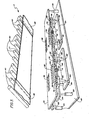
- FIG 2 is a perspective view showing the rear exterior configuration of the deposition apparatus 2 in which a continuous web of substrate material 11 is moved from a supply chamber 96 through the deposition chamber 6 and wound onto a roll in take-up chamber 94.
- the evaporation of a metal occurs by resistively heating the source 4, usually a crucible or other evaporation boat through which electrical current may be passed.
- the source 4 of metallic material 3 may also be inductively heated without departing from the spirit or scope of the p'resent invention.
- the crucible 4 is resistively heated by passing electrical current from a power supply 22 through coils wrapped about the crucible 4.
- Oxygen, from a source 23, adapted to react with the evaporated material 3 is continuously introduced into the deposition chamber 6.
- the method disclosed herein does not require the introduction of a'primary ionizable inert gas to secondarily ionize the oxygen gas. This is because of the more efficient ionization produced by the r.f. power, detailed hereinafter.
- Conventional pumping apparatus 26 vacuumizes the deposition chamber 6 to preselected pressure conditions.
- the reaction between the evaporated metallic material 3 and the oxygen is initiated by an r.f. signal generated by a source of r.f. power 28 which energizes an apertured cathode 30 disposed above the metallic material source 4 in the deposition chamber 6.
- the r.f. signal developes a plasma in the vapor zone or plasma region 5 into which the metallic material 3 is evaporated.
- the vapor zone or region 5 is defined as that area between the source of metallic material 4 and a substrate such as 11. It is in this zone 5 that the ionized metal atoms and ionized oxygen atoms and energetic neutral atoms react with each other and with neutral metal and oxygen atoms to form a metal oxide deposit on the substrate 11.
- the substrate 11, on which the metal oxide film 22 deposits may be slowly moved through the deposition chamber 6 from a feed roller lla to a take-up roller llb. While the continuous deposition of metal oxide film 22 represents one preferred embodiment of the deposition apparatus, the deposition of the metal oxide film 22 in a batch processing mode represents a second preferred embodiment. In the batch processing mode, the metal oxide film 22 is deposited onto a sheet-like or plate-like substrate which is removed from the chamber 6 once a coating 22 of preselected thickness has been deposited. Infrared lamps 40 and a heat reflector 42 cooperate to raise the temperature of the substrate 11, whether in plate or roll form, to, and maintain the temperature thereof, at a preselected level.
- the rate at which the substrate 11 moves through the deposition chamber 6 depends upon the desired thickness of the metal oxide film 22 to be deposited.
- a quartz crystal thickness monitor 34 of convention specification may be employed to gauge the thickness of the metal oxide film 22 during the deposition process.
- the thickness of metal oxide deposited onto the substrate 11 can be adjusted by adjusting the speed of substrate movement through the vapor region 5 of the deposition chamber 6.
- the deposition chamber 6, shown schematically in Figure 2 is adapted for the depositon of the metal oxide film 22 onto a stationary substrate 11.
- a pair of shelves 45 (partially shown) support the substrate 11 in a position elevated above the sources of metallic material 4.
- a pluralty of sources 4 of the metallic material 3 are provided.
- four sources 4 are provided to evaporate the metallic material 3, through four corresponding apertures 35 in the r.f. powered cathode 30. The operation of the four apertures will be-discussed in a later section with specific reference to Figure 4.
- the apparatus is equally adapted for use with the continuous roll of substrate material illustrated and discussed supra with respect to Figure 2. If used with the continuous roll of substrate material, the shelves 45 would serve as shields to define the length of substrate 11 upon which the metal oxide film could be continuously deposited.
- a platform 46 which can be formed of stainless steel, is supported adjacent the lower portion of the deposition chamber 6.
- the platform 46 is shown diagrammatically for the sake of clarity, whereas in Figure 5 the construction thereof is detailed.
- Four vertically adjustable legs 50 extend from the platform 46.
- the legs 50 are fabricated from ceramic material for electrically insulating the stainless steel cathode 30, which they support, from the stainless steel platform 46.
- the platform 46 may further be provided with holes 52 along the back end thereof for fluidic intercommunication of portions of the deposition chamber 6 above and below the platform 46.
- a plurality of substantially identical bases 54 are spacedly affixed to the platform 46.
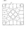
- four equally spaced platforms are provided, however, the number and spacing of the platforms is dependent upon the size and configuration of the substrate upon which the metal oxide film 22 is to be deposited. This will become more clear from the description of Figure 4 wherein the uniformity of deposition is discussed.
- Each of the bases.54 includes a set of electrically insulating ceramic pillars 62 and a. set of electrically conductive pillars 64. Associated with each set of pillars, 62 and 64, is a connecting block 66, preferably formed of copper; a pair of clamps 68, preferably formed of copper; and a plurality of screws 20.
- the crucible 4, or other like source, with a tungsten coil 82 wound thereabout, is suspended between the clamping apparatus of each of the bases 54. More particularly, one end of a first braided copper lead 84 is attached to one end of the tungsten coil 82, while the other end of each copper lead 84 is sandwiched between a clamping element 68 and the connector block 66.
- a second braided copper lead 86 is likewise sandwiched between a clamping element 68 and the opposite connector block 66. In this manner power from the electrical power supply 22, illustrated in and previously discussed with reference to Figure 2, is received by the tungsten coil 82. Note that the side of the crucible 4 opposite the "hot" side is grounded because the conductive pillars 64 to which the leads 84 are secured are grounded.
- the crucibles 4 are resistively heated by the power supply 22, thereby intiating evaporation of the metallic material 3 therefrom.
- the evaporated metallic material 3 passes through the openings or apertures 35 formed in the cathode 30 and into the deposition region 5 of the deposition chamber 6.
- the r.f. power produces an ionized plasma in the deposition region 5 from the oxygen gas 23 introduced thereonto and the metallic material 3 evaported thereinto.
- the ionized metal oxide is then deposited onto the surface of the substrate 11 disposed thereabove.
- a plate-like substrate 11 is illustrated.
- Deposited onto one surface o'f the substrate is the thin film 22 of transmissive, conductive metal oxide material.
- a plurality of sources of metallic material are provided in the.deposition chamber 6.
- sources of material each preferably disposed about eighteen inches below the substrate 11 and equally spaced about eleven inches from one another are provided. It has been found that with the foregoing spacial relationship of metallic material sources relative to the substrate and relative to each adjacent source, the metallic film 22 is uniformly deposited onto the substrate.
- each of the regions has deposited thereon approximately the same amount of metal oxide material, the regions vary in the amount of material contributed from each of the four sources. More particularly, the .ionized metal-oxide from the vapor zone 5 is deposited onto the surface of the substrate plate 11 in regions. These regions vary in thickness of film deposited (from an individual one of the sources) from circular regions A which directly overlie each of the sources 4; to first ring-like regions B which are radially removed from circular regions A; to second ring-like regions C which are radially removed from regions B; to third ring-like regions D which are radially removed from regions C; to fourth ring-like regions E which are radially removed from regions D.
- indium and tin compositions Numerous tests were performed with indium and tin compositions in order to form an In 2 0 3 --Sn doped film.
- the indium-tin alloys were formed by melting indium in a vacuum and then quenching. The ratio between the weight of indium divided by indium's atomic weight and the weight of tin divided by tin's atomic weight, was 85/15.
- Many other compositions were tested, ranging from 100% indium to indium with 50% tin.
- the substrates were both stationary and made of glass; a vacuum of about 10 -5 torr was establihsed before the introduction of oxygen; the metal source to substrate distance was about 18 inches; the frequency of r.f. signal was 13.56 megahertz; and r.f. power was about 100 watts.
- the following example employed tin and antimony as the metallic material which is evaporated.
- the starting vacuum was about 10 -5 torr; the net r.f. power was about 100 watts, the r.f. frequency was 13.56 megahertz; and the source to substrate distance was.about 18 inches.
- the following example was performed with zinc as the sole evaporated material, with an initial vacuum pressure of 10 -5 torr, a net r.f. power of about 100 watts, an r.f. frequency of 13.56 megahertz, and a source to substrate distance of about 18 inches.
Landscapes
- Engineering & Computer Science (AREA)
- Chemical & Material Sciences (AREA)
- Physics & Mathematics (AREA)
- Condensed Matter Physics & Semiconductors (AREA)
- Electromagnetism (AREA)
- General Physics & Mathematics (AREA)
- Computer Hardware Design (AREA)
- Microelectronics & Electronic Packaging (AREA)
- Power Engineering (AREA)
- Manufacturing & Machinery (AREA)
- Chemical Kinetics & Catalysis (AREA)
- Materials Engineering (AREA)
- Mechanical Engineering (AREA)
- Metallurgy (AREA)
- Organic Chemistry (AREA)
- Photovoltaic Devices (AREA)
- Physical Vapour Deposition (AREA)
- Manufacturing Of Electric Cables (AREA)
- Chemical Vapour Deposition (AREA)
- Electrodes Of Semiconductors (AREA)
- Physical Deposition Of Substances That Are Components Of Semiconductor Devices (AREA)
- Non-Insulated Conductors (AREA)
Applications Claiming Priority (2)
| Application Number | Priority Date | Filing Date | Title |
|---|---|---|---|
| US06/448,139 US4605565A (en) | 1982-12-09 | 1982-12-09 | Method of depositing a highly conductive, highly transmissive film |
| US448139 | 1982-12-09 |
Publications (3)
| Publication Number | Publication Date |
|---|---|
| EP0112132A2 true EP0112132A2 (fr) | 1984-06-27 |
| EP0112132A3 EP0112132A3 (en) | 1985-07-03 |
| EP0112132B1 EP0112132B1 (fr) | 1989-03-22 |
Family
ID=23779157
Family Applications (1)
| Application Number | Title | Priority Date | Filing Date |
|---|---|---|---|
| EP83307497A Expired EP0112132B1 (fr) | 1982-12-09 | 1983-12-08 | Procédé pour le dépôt d'une couche hautement conductrice et hautement transparente |
Country Status (12)
| Country | Link |
|---|---|
| US (1) | US4605565A (fr) |
| EP (1) | EP0112132B1 (fr) |
| JP (1) | JPH0622202B2 (fr) |
| KR (1) | KR910007380B1 (fr) |
| AU (1) | AU564776B2 (fr) |
| BR (1) | BR8306745A (fr) |
| CA (1) | CA1219968A (fr) |
| DE (1) | DE3379489D1 (fr) |
| ES (2) | ES8505838A1 (fr) |
| IN (1) | IN163675B (fr) |
| MX (1) | MX155196A (fr) |
| ZA (1) | ZA838885B (fr) |
Cited By (6)
| Publication number | Priority date | Publication date | Assignee | Title |
|---|---|---|---|---|
| EP0161088A1 (fr) * | 1984-05-02 | 1985-11-13 | Energy Conversion Devices, Inc. | Appareil pour le dépôt de couches minces à l'aide de plasma |
| EP0167446A2 (fr) * | 1984-07-02 | 1986-01-08 | EASTMAN KODAK COMPANY (a New Jersey corporation) | Matériau semi-conducteur et substrat |
| EP0261245A1 (fr) * | 1986-03-12 | 1988-03-30 | Tobi Co., Ltd. | Procede de production d'un film conducteur transparent |
| EP0263880A1 (fr) * | 1986-03-12 | 1988-04-20 | Tobi Co., Ltd. | Dispositif de plaquage ionique continu pour un film a defilement rapide |
| EP0326178A2 (fr) * | 1988-01-28 | 1989-08-02 | Hitachi, Ltd. | Méthode de fabrication d'un photodétecteur |
| EP0597670A1 (fr) * | 1992-11-09 | 1994-05-18 | Chugai Ings Co., Ltd | Méthode de fabrication d'un moulage plastique faisant écran aux ondes électromagnétiques |
Families Citing this family (14)
| Publication number | Priority date | Publication date | Assignee | Title |
|---|---|---|---|---|
| US4842705A (en) * | 1987-06-04 | 1989-06-27 | Siemens Aktiengesellschaft | Method for manufacturing transparent conductive indium-tin oxide layers |
| US5008215A (en) * | 1989-07-07 | 1991-04-16 | Industrial Technology Research Institute | Process for preparing high sensitivity semiconductive magnetoresistance element |
| US5698262A (en) * | 1996-05-06 | 1997-12-16 | Libbey-Owens-Ford Co. | Method for forming tin oxide coating on glass |
| US6153271A (en) * | 1999-12-30 | 2000-11-28 | General Vacuum, Inc. | Electron beam evaporation of transparent indium tin oxide |
| KR20010078862A (ko) * | 2001-05-02 | 2001-08-22 | 조육형 | 산화물 증착 플라스틱 필름의 연속 열처리 방법 및 시스템 |
| EP1289025A1 (fr) * | 2001-08-30 | 2003-03-05 | Universite De Neuchatel | Procédé de dépot d'une couche d'oxyde sur un substrat et cellule photovoltaique utilisant ce substrat |
| ATE488614T1 (de) * | 2002-08-28 | 2010-12-15 | Moxtronics Inc | Hybridstrahl-beschichtungssystem und verfahren zur herstellung von zno-schichten |
| WO2004072329A1 (fr) * | 2003-02-14 | 2004-08-26 | The University Of Hong Kong | Dispositif et procede de production d'ozone |
| US20070054158A1 (en) * | 2005-09-07 | 2007-03-08 | Ovshinsky Stanford R | Combination of photovoltaic devices and batteries which utilize a solid polymeric electrolyte |
| US9276142B2 (en) | 2010-12-17 | 2016-03-01 | First Solar, Inc. | Methods for forming a transparent oxide layer for a photovoltaic device |
| US8476105B2 (en) | 2010-12-22 | 2013-07-02 | General Electric Company | Method of making a transparent conductive oxide layer and a photovoltaic device |
| JP2014107421A (ja) * | 2012-11-28 | 2014-06-09 | Shimadzu Corp | 成膜装置、放射線検出器および放射線検出器の製造方法 |
| US10270010B2 (en) | 2014-01-28 | 2019-04-23 | Kaneka Corporation | Substrate with transparent electrode and method for producing same |
| RU2609764C1 (ru) * | 2015-10-26 | 2017-02-02 | Федеральное государственное автономное образовательное учреждение высшего образования "Национальный исследовательский университет "Московский институт электронной техники" (МИЭТ) | Способ получения аморфных пленок халькогенидных стеклообразных полупроводников с эффектом фазовой памяти |
Citations (2)
| Publication number | Priority date | Publication date | Assignee | Title |
|---|---|---|---|---|
| EP0049586A1 (fr) * | 1980-10-06 | 1982-04-14 | Optical Coating Laboratory, Inc. | Procédé et appareil pour la formation de couches d'oxyde très minces en utilisant la technique d'évaporation réactive |
| EP0060363A1 (fr) * | 1981-03-16 | 1982-09-22 | Exxon Research And Engineering Company | Procédé de fabrication d'un dispositif semiconducteur PIN en silicium amorphe |
Family Cites Families (4)
| Publication number | Priority date | Publication date | Assignee | Title |
|---|---|---|---|---|
| US4170662A (en) * | 1974-11-05 | 1979-10-09 | Eastman Kodak Company | Plasma plating |
| US4342631A (en) * | 1980-06-16 | 1982-08-03 | Illinois Tool Works Inc. | Gasless ion plating process and apparatus |
| US4336277A (en) * | 1980-09-29 | 1982-06-22 | The Regents Of The University Of California | Transparent electrical conducting films by activated reactive evaporation |
| JPS5880877A (ja) * | 1981-11-10 | 1983-05-16 | Konishiroku Photo Ind Co Ltd | 太陽電池及びその製造方法 |
-
1982
- 1982-12-09 US US06/448,139 patent/US4605565A/en not_active Expired - Lifetime
-
1983
- 1983-11-29 ZA ZA838885A patent/ZA838885B/xx unknown
- 1983-11-30 IN IN801/DEL/83A patent/IN163675B/en unknown
- 1983-12-06 ES ES527828A patent/ES8505838A1/es not_active Expired
- 1983-12-08 JP JP58232222A patent/JPH0622202B2/ja not_active Expired - Lifetime
- 1983-12-08 DE DE8383307497T patent/DE3379489D1/de not_active Expired
- 1983-12-08 BR BR8306745A patent/BR8306745A/pt unknown
- 1983-12-08 EP EP83307497A patent/EP0112132B1/fr not_active Expired
- 1983-12-08 MX MX199667A patent/MX155196A/es unknown
- 1983-12-08 AU AU22231/83A patent/AU564776B2/en not_active Ceased
- 1983-12-08 KR KR1019830005817A patent/KR910007380B1/ko not_active IP Right Cessation
- 1983-12-08 CA CA000442836A patent/CA1219968A/fr not_active Expired
-
1985
- 1985-02-12 ES ES540320A patent/ES8700977A1/es not_active Expired
Patent Citations (2)
| Publication number | Priority date | Publication date | Assignee | Title |
|---|---|---|---|---|
| EP0049586A1 (fr) * | 1980-10-06 | 1982-04-14 | Optical Coating Laboratory, Inc. | Procédé et appareil pour la formation de couches d'oxyde très minces en utilisant la technique d'évaporation réactive |
| EP0060363A1 (fr) * | 1981-03-16 | 1982-09-22 | Exxon Research And Engineering Company | Procédé de fabrication d'un dispositif semiconducteur PIN en silicium amorphe |
Non-Patent Citations (6)
| Title |
|---|
| APPLIED PHYSICS LETTERS, vol.35, no.2, July 1979, pages 161-162, NEW YORK, (US) R. HOWSON et al.: "Properties of conducting transparent oxide films produced by ion plating onto room-temperature substrates". * |
| PATENTS ABSTRACTS OF JAPAN, vol. 6, no.68, (C-100) (946) April 30, 1982 * |
| PATENTS ABSTRACTS OF JAPAN, vol.1, no.102, September 10, 1977, page 2322 C 77. * |
| PATENTS ABSTRACTS OF JAPAN, vol.1, no.102, September 10, 1977, page 2322 C 77. & JP-A-52 065 183 (MATSUSHITA DENKI SANGYO K.K.) (30-05-1977) * |
| PATENTS ABSTRACTS OF JAPAN, vol.6, no.68, (C-100) (946) April 30, 1982. * |
| PATENTS ABSTRACTS OF JAPAN, vol.6, no.68, (C-100) (946) April 30, 1982. & JP-A-57 005 865 (KONISHIROKU SHASHIN KOGYO K.K.) (12-01-1982) * |
Cited By (10)
| Publication number | Priority date | Publication date | Assignee | Title |
|---|---|---|---|---|
| EP0161088A1 (fr) * | 1984-05-02 | 1985-11-13 | Energy Conversion Devices, Inc. | Appareil pour le dépôt de couches minces à l'aide de plasma |
| EP0167446A2 (fr) * | 1984-07-02 | 1986-01-08 | EASTMAN KODAK COMPANY (a New Jersey corporation) | Matériau semi-conducteur et substrat |
| EP0167446A3 (en) * | 1984-07-02 | 1988-08-31 | Eastman Kodak Company | Semiconductor material and substrate |
| EP0261245A1 (fr) * | 1986-03-12 | 1988-03-30 | Tobi Co., Ltd. | Procede de production d'un film conducteur transparent |
| EP0263880A1 (fr) * | 1986-03-12 | 1988-04-20 | Tobi Co., Ltd. | Dispositif de plaquage ionique continu pour un film a defilement rapide |
| EP0263880A4 (fr) * | 1986-03-12 | 1989-01-12 | Tobi Co Ltd | Dispositif de plaquage ionique continu pour un film a defilement rapide. |
| EP0261245A4 (fr) * | 1986-03-12 | 1989-01-12 | Tobi Co Ltd | Procede de production d'un film conducteur transparent. |
| EP0326178A2 (fr) * | 1988-01-28 | 1989-08-02 | Hitachi, Ltd. | Méthode de fabrication d'un photodétecteur |
| EP0326178A3 (en) * | 1988-01-28 | 1990-06-27 | Hitachi, Ltd. | Method of making a photosensor |
| EP0597670A1 (fr) * | 1992-11-09 | 1994-05-18 | Chugai Ings Co., Ltd | Méthode de fabrication d'un moulage plastique faisant écran aux ondes électromagnétiques |
Also Published As
| Publication number | Publication date |
|---|---|
| KR850003480A (ko) | 1985-06-17 |
| ES527828A0 (es) | 1985-06-16 |
| AU2223183A (en) | 1984-06-14 |
| DE3379489D1 (en) | 1989-04-27 |
| US4605565A (en) | 1986-08-12 |
| EP0112132A3 (en) | 1985-07-03 |
| BR8306745A (pt) | 1984-07-17 |
| MX155196A (es) | 1988-02-01 |
| KR910007380B1 (ko) | 1991-09-25 |
| IN163675B (fr) | 1988-10-29 |
| ES8505838A1 (es) | 1985-06-16 |
| JPH0622202B2 (ja) | 1994-03-23 |
| ES540320A0 (es) | 1986-11-16 |
| ES8700977A1 (es) | 1986-11-16 |
| AU564776B2 (en) | 1987-08-27 |
| EP0112132B1 (fr) | 1989-03-22 |
| JPS59117178A (ja) | 1984-07-06 |
| CA1219968A (fr) | 1987-03-31 |
| ZA838885B (en) | 1984-07-25 |
Similar Documents
| Publication | Publication Date | Title |
|---|---|---|
| US4605565A (en) | Method of depositing a highly conductive, highly transmissive film | |
| US4728406A (en) | Method for plasma - coating a semiconductor body | |
| US4514437A (en) | Apparatus for plasma assisted evaporation of thin films and corresponding method of deposition | |
| EP0002383B1 (fr) | Procédé et dispositif pour le dépôt de couches de matériaux semi-conducteurs ou autres | |
| US4678679A (en) | Continuous deposition of activated process gases | |
| US5346853A (en) | Microwave energized deposition process with substrate temperature control for the fabrication of P-I-N photovoltaic devices | |
| US4402762A (en) | Method of making highly stable modified amorphous silicon and germanium films | |
| US4798167A (en) | Apparatus for preparing a photoelectromotive force member having a concentric triplicate conduit for generating active species and precursor | |
| EP0099257A1 (fr) | Appareil pour le chauffage uniforme d'un substrat | |
| US4440107A (en) | Magnetic apparatus for reducing substrate warpage | |
| US5342452A (en) | Photovoltaic device | |
| US5487786A (en) | Plasma chemical vapor deposition device capable of suppressing generation of polysilane powder | |
| EP0228870B1 (fr) | Méthode de fabrication d'une couche déposée | |
| EP0121443A2 (fr) | Dispositif et méthode pour le dépôt continu d'un film très conducteur et très transparent | |
| US4766091A (en) | Method for producing an electronic device having a multi-layer structure | |
| JP3027670B2 (ja) | 光起電力素子 | |
| JP3406959B2 (ja) | マイクロ波プラズマcvd法による堆積膜形成方法 | |
| JP2000004036A (ja) | 微結晶半導体層の形成方法、および光起電力素子 | |
| JP2785884B2 (ja) | 光起電力素子 | |
| JP2984430B2 (ja) | 光起電力素子 | |
| US20100116334A1 (en) | Vhf energized plasma deposition process for the preparation of thin film materials | |
| JP2862416B2 (ja) | 光起電力素子 | |
| US20100117172A1 (en) | Thin film semiconductor alloy material prepared by a vhf energized plasma deposition process | |
| JP2006237180A (ja) | 光起電力素子の形成方法 | |
| JPH01731A (ja) | 堆積膜形成装置 |
Legal Events
| Date | Code | Title | Description |
|---|---|---|---|
| PUAI | Public reference made under article 153(3) epc to a published international application that has entered the european phase |
Free format text: ORIGINAL CODE: 0009012 |
|
| AK | Designated contracting states |
Designated state(s): BE CH DE FR GB IT LI NL |
|
| PUAL | Search report despatched |
Free format text: ORIGINAL CODE: 0009013 |
|
| AK | Designated contracting states |
Designated state(s): BE CH DE FR GB IT LI NL |
|
| 17P | Request for examination filed |
Effective date: 19850917 |
|
| 17Q | First examination report despatched |
Effective date: 19870318 |
|
| GRAA | (expected) grant |
Free format text: ORIGINAL CODE: 0009210 |
|
| AK | Designated contracting states |
Kind code of ref document: B1 Designated state(s): BE CH DE FR GB IT LI NL |
|
| PG25 | Lapsed in a contracting state [announced via postgrant information from national office to epo] |
Ref country code: NL Effective date: 19890322 Ref country code: IT Free format text: LAPSE BECAUSE OF FAILURE TO SUBMIT A TRANSLATION OF THE DESCRIPTION OR TO PAY THE FEE WITHIN THE PRESCRIBED TIME-LIMIT;WARNING: LAPSES OF ITALIAN PATENTS WITH EFFECTIVE DATE BEFORE 2007 MAY HAVE OCCURRED AT ANY TIME BEFORE 2007. THE CORRECT EFFECTIVE DATE MAY BE DIFFERENT FROM THE ONE RECORDED. Effective date: 19890322 Ref country code: BE Effective date: 19890322 |
|
| REF | Corresponds to: |
Ref document number: 3379489 Country of ref document: DE Date of ref document: 19890427 |
|
| ET | Fr: translation filed | ||
| REG | Reference to a national code |
Ref country code: CH Ref legal event code: PL |
|
| NLV1 | Nl: lapsed or annulled due to failure to fulfill the requirements of art. 29p and 29m of the patents act | ||
| PLBI | Opposition filed |
Free format text: ORIGINAL CODE: 0009260 |
|
| PG25 | Lapsed in a contracting state [announced via postgrant information from national office to epo] |
Ref country code: LI Free format text: LAPSE BECAUSE OF NON-PAYMENT OF DUE FEES Effective date: 19891231 Ref country code: CH Free format text: LAPSE BECAUSE OF NON-PAYMENT OF DUE FEES Effective date: 19891231 |
|
| 26 | Opposition filed |
Opponent name: LEYBOLD AKTIENGESELLSCHAFT Effective date: 19891206 |
|
| PGFP | Annual fee paid to national office [announced via postgrant information from national office to epo] |
Ref country code: GB Payment date: 19901119 Year of fee payment: 8 |
|
| PGFP | Annual fee paid to national office [announced via postgrant information from national office to epo] |
Ref country code: DE Payment date: 19901221 Year of fee payment: 8 |
|
| RDAG | Patent revoked |
Free format text: ORIGINAL CODE: 0009271 |
|
| STAA | Information on the status of an ep patent application or granted ep patent |
Free format text: STATUS: PATENT REVOKED |
|
| REG | Reference to a national code |
Ref country code: CH Ref legal event code: PL |
|
| 27W | Patent revoked |
Effective date: 19910417 |
|
| GBPR | Gb: patent revoked under art. 102 of the ep convention designating the uk as contracting state | ||
| PGFP | Annual fee paid to national office [announced via postgrant information from national office to epo] |
Ref country code: FR Payment date: 19911212 Year of fee payment: 9 |