EP0111365B1 - Alimentation à découpage à deux états - Google Patents
Alimentation à découpage à deux états Download PDFInfo
- Publication number
- EP0111365B1 EP0111365B1 EP83201701A EP83201701A EP0111365B1 EP 0111365 B1 EP0111365 B1 EP 0111365B1 EP 83201701 A EP83201701 A EP 83201701A EP 83201701 A EP83201701 A EP 83201701A EP 0111365 B1 EP0111365 B1 EP 0111365B1
- Authority
- EP
- European Patent Office
- Prior art keywords
- voltage
- state
- circuit
- terminal
- source
- Prior art date
- Legal status (The legal status is an assumption and is not a legal conclusion. Google has not performed a legal analysis and makes no representation as to the accuracy of the status listed.)
- Expired
Links
Images
Classifications
-
- H—ELECTRICITY
- H02—GENERATION; CONVERSION OR DISTRIBUTION OF ELECTRIC POWER
- H02M—APPARATUS FOR CONVERSION BETWEEN AC AND AC, BETWEEN AC AND DC, OR BETWEEN DC AND DC, AND FOR USE WITH MAINS OR SIMILAR POWER SUPPLY SYSTEMS; CONVERSION OF DC OR AC INPUT POWER INTO SURGE OUTPUT POWER; CONTROL OR REGULATION THEREOF
- H02M3/00—Conversion of dc power input into dc power output
- H02M3/22—Conversion of dc power input into dc power output with intermediate conversion into ac
- H02M3/24—Conversion of dc power input into dc power output with intermediate conversion into ac by static converters
- H02M3/28—Conversion of dc power input into dc power output with intermediate conversion into ac by static converters using discharge tubes with control electrode or semiconductor devices with control electrode to produce the intermediate ac
- H02M3/325—Conversion of dc power input into dc power output with intermediate conversion into ac by static converters using discharge tubes with control electrode or semiconductor devices with control electrode to produce the intermediate ac using devices of a triode or a transistor type requiring continuous application of a control signal
- H02M3/335—Conversion of dc power input into dc power output with intermediate conversion into ac by static converters using discharge tubes with control electrode or semiconductor devices with control electrode to produce the intermediate ac using devices of a triode or a transistor type requiring continuous application of a control signal using semiconductor devices only
- H02M3/33561—Conversion of dc power input into dc power output with intermediate conversion into ac by static converters using discharge tubes with control electrode or semiconductor devices with control electrode to produce the intermediate ac using devices of a triode or a transistor type requiring continuous application of a control signal using semiconductor devices only having more than one ouput with independent control
-
- G—PHYSICS
- G05—CONTROLLING; REGULATING
- G05F—SYSTEMS FOR REGULATING ELECTRIC OR MAGNETIC VARIABLES
- G05F3/00—Non-retroactive systems for regulating electric variables by using an uncontrolled element, or an uncontrolled combination of elements, such element or such combination having self-regulating properties
- G05F3/02—Regulating voltage or current
-
- H—ELECTRICITY
- H02—GENERATION; CONVERSION OR DISTRIBUTION OF ELECTRIC POWER
- H02M—APPARATUS FOR CONVERSION BETWEEN AC AND AC, BETWEEN AC AND DC, OR BETWEEN DC AND DC, AND FOR USE WITH MAINS OR SIMILAR POWER SUPPLY SYSTEMS; CONVERSION OF DC OR AC INPUT POWER INTO SURGE OUTPUT POWER; CONTROL OR REGULATION THEREOF
- H02M3/00—Conversion of dc power input into dc power output
- H02M3/22—Conversion of dc power input into dc power output with intermediate conversion into ac
- H02M3/24—Conversion of dc power input into dc power output with intermediate conversion into ac by static converters
- H02M3/28—Conversion of dc power input into dc power output with intermediate conversion into ac by static converters using discharge tubes with control electrode or semiconductor devices with control electrode to produce the intermediate ac
- H02M3/325—Conversion of dc power input into dc power output with intermediate conversion into ac by static converters using discharge tubes with control electrode or semiconductor devices with control electrode to produce the intermediate ac using devices of a triode or a transistor type requiring continuous application of a control signal
- H02M3/335—Conversion of dc power input into dc power output with intermediate conversion into ac by static converters using discharge tubes with control electrode or semiconductor devices with control electrode to produce the intermediate ac using devices of a triode or a transistor type requiring continuous application of a control signal using semiconductor devices only
- H02M3/33507—Conversion of dc power input into dc power output with intermediate conversion into ac by static converters using discharge tubes with control electrode or semiconductor devices with control electrode to produce the intermediate ac using devices of a triode or a transistor type requiring continuous application of a control signal using semiconductor devices only with automatic control of the output voltage or current, e.g. flyback converters
- H02M3/33523—Conversion of dc power input into dc power output with intermediate conversion into ac by static converters using discharge tubes with control electrode or semiconductor devices with control electrode to produce the intermediate ac using devices of a triode or a transistor type requiring continuous application of a control signal using semiconductor devices only with automatic control of the output voltage or current, e.g. flyback converters with galvanic isolation between input and output of both the power stage and the feedback loop
-
- H—ELECTRICITY
- H02—GENERATION; CONVERSION OR DISTRIBUTION OF ELECTRIC POWER
- H02M—APPARATUS FOR CONVERSION BETWEEN AC AND AC, BETWEEN AC AND DC, OR BETWEEN DC AND DC, AND FOR USE WITH MAINS OR SIMILAR POWER SUPPLY SYSTEMS; CONVERSION OF DC OR AC INPUT POWER INTO SURGE OUTPUT POWER; CONTROL OR REGULATION THEREOF
- H02M1/00—Details of apparatus for conversion
- H02M1/0003—Details of control, feedback or regulation circuits
- H02M1/0032—Control circuits allowing low power mode operation, e.g. in standby mode
-
- Y—GENERAL TAGGING OF NEW TECHNOLOGICAL DEVELOPMENTS; GENERAL TAGGING OF CROSS-SECTIONAL TECHNOLOGIES SPANNING OVER SEVERAL SECTIONS OF THE IPC; TECHNICAL SUBJECTS COVERED BY FORMER USPC CROSS-REFERENCE ART COLLECTIONS [XRACs] AND DIGESTS
- Y02—TECHNOLOGIES OR APPLICATIONS FOR MITIGATION OR ADAPTATION AGAINST CLIMATE CHANGE
- Y02B—CLIMATE CHANGE MITIGATION TECHNOLOGIES RELATED TO BUILDINGS, e.g. HOUSING, HOUSE APPLIANCES OR RELATED END-USER APPLICATIONS
- Y02B70/00—Technologies for an efficient end-user side electric power management and consumption
- Y02B70/10—Technologies improving the efficiency by using switched-mode power supplies [SMPS], i.e. efficient power electronics conversion e.g. power factor correction or reduction of losses in power supplies or efficient standby modes
Definitions
- the invention relates to a switching power supply circuit, comprising a first and a second voltage source, each being connectable respectively to a first and a second output terminal, and first regulating means for acting on the switching when a voltage exceeds a first reference value, said supply circuit being capable of working on demand either in a first state in which the first voltage source connected to the first output terminal supplies it with a first voltage and the second voltage source connected to the second output terminal applies a second voltage thereto which is greater than the first voltage, ie in a second state in which the voltage applied to the first terminal is practically the same as in the first state, however that the voltage applied to the second terminal is smaller than that applied to it in the first state.
- Circuits of the type concerned by the invention are used in particular in televisions fitted with a remote control. They can be in two states corresponding either to normal operation of the television set, or to the so-called standby mode, in which the receiving circuits of the remote control commands remain supplied normally, while the other circuits are supplied under reduced voltage or even are no longer powered at all.
- German patent DE-A-2 620191 discloses a more satisfactory circuit, in which one of the windings of a switching power supply transformer is wound in the opposite direction to the others. As a result, the voltages from this winding do not depend on the switching duty cycle. By varying this ratio, it is therefore possible to reduce the other voltages without modifying that from said winding, which is used to power the remote control receiver circuit.
- this system has the disadvantage that the voltage from the inverted winding is not stabilized by the overall stabilization system, and that it is then necessary to provide an additional stabilizing circuit in series in the usual case where the voltage of the sector can vary in important proportions and especially with the current tendency according to which the televisions can be connected without commutation on all the sectors from 90 to 250 volts.
- This stabilizing circuit in addition to its cost, has the drawback of increasing consumption in the standby state.
- the object of the circuit according to the invention is to provide a power supply which does not have any of the drawbacks mentioned above.
- a circuit according to the invention is characterized in that it further comprises second regulation means for supplying a signal which acts on the chopping operation to reduce all at the same time in the same ratio the values of the supplied voltages when a voltage exceeds a second voltage reference and a device for selecting the first or second state, by controlling first and second switching means, said first switching means connecting the second voltage source in the first state to the first means regulating, and in the second state to the second regulating means, and said second switching means connecting the first output terminal, in the first state to the first voltage source, and in the second state to the second voltage source.
- a current limiter is advantageously used with the switching means.
- This limiter is advantageously of a controllable type. l
- the advantage of the invention is that it makes it possible to reduce all but one of the voltages by means of a single switch through which high currents do not pass, all the voltages remaining permanently stabilized and permanently by the single stabilization circuit. .
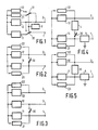
- FIGS 1 to 5 schematically represent different embodiments of the invention.
- Figure 6 shows a detailed diagram of a preferred embodiment.
- the invention can be implemented by means of the circuit of FIG. 1.
- This circuit allows various voltages supplied to several terminals of a switching power supply provided with several voltage sources to be modified simultaneously, these voltages possibly being modified in one direction or in different proportions depending on the limits considered.
- the source voltages are all modified at the same time in the same ratio by means of an inverter which selects a regulation circuit as desired, and, at the same time, at least one connection between a terminal and a source by connection between this same terminal and another source by means of another inverter.
- the voltage of the i of the terminals is modified in a ratio which depends on the regulation circuits, while the voltage of a terminal ai is modified in a different ratio, and even possibly in a different direction, since the source which l feed has changed.
- the regulation circuit 21 is connected to the source 11.
- the source 12 provides a higher voltage than the source 11.
- the regulating circuit 21 is connected to the source 12 and, therefore, the latter takes the voltage that the source 11 previously had, and the voltage of the source 11 is lowered in the same proportion but it no longer delivers since the voltage it can supply is lower than that present on its output.
- the power supply 11 may comprise at least one diode (19, FIG. 6) which prevents a current from entering the voltage source if the voltage across its terminals is higher than that she can deliver.
- the source voltages are therefore all modified at the same time in the same ratio by connecting the regulating circuit 21 to the source 12 instead of the source 11 by the switch 30 and, at the same time, two voltage sources are connected together. 11 and 12, by means of this same switch 30.
- the first regulation means 21 deliver a signal when a supplied voltage exceeds a set value, this signal acting on the switching to decrease together the values of the supplied voltages. These means 21 are connected to terminal 1 and the circuit is provided with switching elements 30 to put the circuit in the second state by connecting, on request, terminal 1 to the second voltage source 12.
- the voltage sources 11 and 12 are designed so that the source 12 supplies a voltage three times that supplied by 11 and that the means 21 limit the voltages supplied when the voltage of the source 11 exceeds the set value 5 volts . At this time, the source 12 supplies 15 volts. If the switch 30 is closed, the means 21 connected to the source 12 limit the voltage of this source to 5 volts. Source 11 can no longer supply more than a third of 5 volts and no longer flows. The two terminals 1 and 2 connected together are now supplied at 5 volts. The voltage of terminal 2 receives a voltage (5 volts, lower than that (15 volts) that it had in the first state, however that a voltage of 5 volts is supplied to terminal 1 and is equal to that it received in the first state.
- second regulation means 22 permanently connected to the second voltage source, for delivering a limitation signal when a supplied voltage exceeds a second set value.
- these means act for a voltage of 12 volts.
- the source 12 cannot therefore supply more than 12 volts to terminal 2 and the source 11 supplies the third, that is 4 volts to terminal 1.
- the means 21 limit the voltage to 5 volts from source 12. Terminal 2 therefore receives the lower voltage (5 volts) than it had in the first state (12 volts), while terminal 1 receives a voltage (5 volts) greater than that (4 volts ) that she had in the first state.
- the switching elements 30 connect, on request, terminal 1 to the source 12.
- the voltages supplied by the source 12 are six times higher and those supplied by the source 13 are three times higher than those supplied by the source 11.
- the means 21 connected to terminal 1 limit the voltages when a supplied voltage exceeds the set value 5 volts
- means 22 connected to terminal 3 limit the voltages when a supplied voltage exceeds the setpoint 14 volts.
- the switch 30 being open, there are, thanks to the action of the means 22, fourteen volts on terminal 3 and on terminals 1 and 2 of the voltages in the ratios provided, namely 4, 66 and 28 volts respectively.
- the means 21 do not act since the voltage on terminal 1 is less than 5 volts. If the switch 30 is closed, the means 21 act and limit the voltage on terminals 1 and 2 together to 5 volts. Then, the source 11 provides 0.8 volts and does not flow, and the source 13 provides 2.5 volts.
- the means 22 no longer act. Circuits (not shown) supplied by terminals 2 and 3 see their voltage considerably decrease in a ratio 5.6 for the example above, while the supply of the standby circuits supplied by terminal 1 is not modified, or slightly increased.
- the means 22 are removed, for example in the circuit of FIG. 3, the respective voltages on the terminals 1, 2, 3 become for the first state 5; 30; 15 volts and for the second state 5; 5; 2.5 volts. In the second state, there is therefore no change.
- the function of the means 22 is to obtain that, in the first state, it is the voltage of the terminal to which they are connected which is regulated with the greatest precision if the circuits which it supplies particularly need a voltage more stable than the others. With a circuit of the kind shown in FIG.
- the ratio of the voltages between terminal 2 with very stable voltage regulated by the means 22 and terminal 1 connected for example to the remote control receiver circuits does not make it possible to obtain a sufficient voltage reduction during the implementation of the method according to the invention, and the means 22 are then preferably connected to a terminal 3 different from that (2) to which the first terminal 1 is connected in the second state, as done in the circuit of figure 3.
- terminal 1 When terminal 1 is connected to voltage source 12, it is to be feared that, before the change in the regulation could have acted, terminal 1 is briefly brought to a voltage dangerous for the circuits which it supplies. This comes, in particular, from the charge accumulated in a capacitor (25, Figure 6) that includes the voltage source 12. In order to avoid damage, it is therefore advantageous to provide a current limitation, and possibly a limitation of the voltage, for terminal 1.
- FIG. 4 shows how, to obtain this effect, a current limiter 4 is inserted between the voltage source 12 and terminal 1, in series with the switching element 30.
- FIG. 5 shows an advantageous arrangement in which all of the switching means 30 and the limiter 4 has been combined in a controllable current limiter 6 which then constitutes the above switching means.
- the reference 5 indicates a voltage limiting circuit via which the connection is made from terminal 1 to the switching elements 6 or 30 and to the voltage source 11.
- This circuit 5 does not constitute a stabilizer voltage, but only has the role of limiting the voltage at terminal 1 to a value compatible with circuit safety.
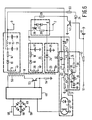
- FIG. 6 shows in detail a preferred embodiment of the invention which corresponds substantially to the circuit of FIG. 3, further provided with circuits 5 and 6 of FIG. 5.
- the circuits 11, 12, 13, 21, 5, 6 of the preceding figures are indicated by frames in dotted lines.
- the means 21 and 22 use a common part (44 to 47) to act on the cutting and to decrease the values of the supplied voltages.
- the mains voltage is brought to terminals 50; it is rectified by diodes 49 connected in bridge and smoothed by a capacitor 56 and the voltage obtained is applied to a known circuit 48 which controls the cutting.
- This circuit 48 which comprises for example a TEA 1039 integrated circuit marketed by the company RTC LA RADIOTECHNIQUE-COMPELEC and intended for the control and regulation of switching power supplies, supplies a switching transistor 53 with its basic control voltage and receives in return information on the current of said transistor, measured by an emitter resistance 54.
- the primary winding 55 of a supply transformer 8 is inserted into the collector of transistor 53.
- Circuit 48 also receives a signal d a photocoupler 47, signal acting on the chopping to decrease together the values of the voltages supplied to secondary windings 9, 20, 23 of the transformer 8. This signal acts, in known manner, by modifying the form factor of the applied control pulses at the base of transistor 53.
- the photocoupler provides galvanic isolation between the mains and the TV circuits.
- the means 22 consist of the photocoupler 47 connected to a socket on a resistor chain 57, 44, 45, 46 one end of which is connected to ground and the other to the anode of a Zener diode 58 whose cathode is connected to the voltage source 13. The location of the outlet is chosen so that the voltage of the source 13 is adjusted to 14 volts.
- the means 21 are constituted by the same constituents 44 to 47 and a diode 43 whose cathode is connected to the common point of the resistors 44 and 57, and whose anode is connected to the voltage source 11.
- the values of the resistors are chosen so that, when the means 22 act with respect to a reference voltage 14 volts, the means 21 act for a voltage of the order of 5.5 volts.
- the three positive voltage sources 11, 12, 13 each consist respectively of a winding 20, 23, 9 of the transformer 8 which supplies a rectifying diode 19, 24, 10, respectively, and a filtering capacitor 17, 25, 15 , respectively. Fuses 14 and 18 can be provided.
- the source 13 further comprises an inductor 16 between two capacitors 15. These three voltage sources are perfectly known to those skilled in the art.
- the three windings 20, 23, 9 are wound in the same direction with respect to their end connected to ground so as to provide inductive current during the blocking phases of transistor 53.
- the ratios of the number of turns of the windings 9, 20 , 23 are such that the voltage source 11 supplies approximately 5 volts, when the voltage source 13 supplies 14 volts (thanks to the action of the means 22) and the voltage source 12 supplies approximately 30 volts.
- Each terminal 1,2,3 3 is joined respectively to an output of the voltage sources 11, 12, 13.
- the sources 11 and 12 are joined together on demand by the circuit 6.
- the latter contains a PNP transistor 26 whose collector is joined to the source 11 and whose emitter is joined, via a resistor 28, to the source 12 and at terminal 2.
- Two diodes 27 are connected in series between terminal 2 and the base of transistor 26. They are conductive when terminal 2 is positive with respect to the base of transistor 26. Their role is to limit so known the current in the resistor 28 to a value such that the voltage across this resistor is substantially equal to the direct voltage drop across a diode.
- circuit 6 constitutes a current limiter.
- the transistor 26 is, moreover, made conductive on demand when an adequate signal is applied to a terminal 51.
- Such a signal is positive and is applied via an RC cell 40, 41 at the base of an NPN transistor 42 of which the emitter is connected to ground this transistor becomes conductive and controls, via a resistor 29 placed between its collector and the base of the transistor 26, the conduction of the transistor 26.
- the purpose of this RC circuit 40, 41 is to slightly delay the setting in conduction of circuit 6. Circuit 6 is thus a limited current switch, controllable by a signal applied to terminal 51.
- a voltage limiting circuit 5 Between the terminal 1 and the voltage source 11 is inserted a voltage limiting circuit 5. It consists of an NPN transistor 38 whose emitter is connected to terminal 1 and whose collector is connected to the voltage source 11. The base of this transistor 38 is connected to ground by two head-to-tail diodes 35, 36, the cathode of the diode 36 which is a Zener diode being on the side of the base. The current for this Zener diode is supplied by a resistor 39 connecting the cathode of diode 36 to the voltage source 11, and also by a diode 34 in series with a resistor 33, connecting the cathode of Zener diode 36 to the source voltage 13. A capacitor 37 of large capacity, in parallel with the diodes 35, 36, makes it possible to obtain a lower dynamic impedance.
- the transistor 26 When a positive signal is applied to terminal 51, the transistor 26 becomes conductive and the voltage source 12 flows to terminal 1, but the current is however limited by the resistor 28. It is however sufficient to make the diode 43 conductive, which produces a signal transmitted by the photocoupler 47 which decreases the voltages supplied, this until the voltage of the source 12 has dropped to around 5.5 volts instead of 30 volts previously. At this time, the voltages from sources 11 and 13 are reduced in the same ratio. The source 11 can no longer supply current since the capacitor 17 remains charged at 5.5 volts by the connection to the source 12, which blocks the diode 19, and the voltage source 13 supplies approximately 2.6 volts.
- the devices connected to terminals 2 and 3 which received 30 and 14 volts respectively are now in standby mode with a supply of respectively 5, 6 and 2.6 volts, while the remote control circuits connected to terminal 1 are still , supplied at their nominal voltage of 5.5 to 5.6 volts.
Landscapes
- Engineering & Computer Science (AREA)
- Power Engineering (AREA)
- Physics & Mathematics (AREA)
- Electromagnetism (AREA)
- General Physics & Mathematics (AREA)
- Radar, Positioning & Navigation (AREA)
- Automation & Control Theory (AREA)
- Direct Current Feeding And Distribution (AREA)
- Dc-Dc Converters (AREA)
- Control Of Voltage And Current In General (AREA)
Applications Claiming Priority (2)
| Application Number | Priority Date | Filing Date | Title |
|---|---|---|---|
| FR8220742A FR2537744A1 (fr) | 1982-12-10 | 1982-12-10 | Procede pour modifier dans des rapports differents diverses tensions d'une alimentation, et alimentation a decoupage a deux etats |
| FR8220742 | 1982-12-10 |
Publications (3)
| Publication Number | Publication Date |
|---|---|
| EP0111365A2 EP0111365A2 (fr) | 1984-06-20 |
| EP0111365A3 EP0111365A3 (en) | 1984-07-25 |
| EP0111365B1 true EP0111365B1 (fr) | 1988-08-10 |
Family
ID=9279968
Family Applications (1)
| Application Number | Title | Priority Date | Filing Date |
|---|---|---|---|
| EP83201701A Expired EP0111365B1 (fr) | 1982-12-10 | 1983-12-01 | Alimentation à découpage à deux états |
Country Status (7)
| Country | Link |
|---|---|
| US (1) | US4631654A (ja) |
| EP (1) | EP0111365B1 (ja) |
| JP (1) | JPH0691747B2 (ja) |
| KR (1) | KR840007644A (ja) |
| DE (1) | DE3377688D1 (ja) |
| FR (1) | FR2537744A1 (ja) |
| HK (1) | HK95191A (ja) |
Families Citing this family (19)
| Publication number | Priority date | Publication date | Assignee | Title |
|---|---|---|---|---|
| US4672516A (en) * | 1985-02-25 | 1987-06-09 | Siemens Aktiengesellschaft | Primary side clock single-ended forward converter with connectible secondary circuits and having switchable actual value feed for the output voltage control |
| US4716488A (en) * | 1985-05-23 | 1987-12-29 | Siemens Aktiengesellschaft | Primary switched-mode power supply unit |
| NL8502338A (nl) * | 1985-08-26 | 1987-03-16 | Philips Nv | Geschakelde voedingsspanningsschakeling met twee toestanden. |
| EP0219736A3 (de) * | 1985-10-17 | 1987-09-23 | Siemens Aktiengesellschaft | Schaltungsanordnung zur Realisierung eines Standby-Betriebs in einem Sperrwandler-Schaltnetzteil |
| FR2605168B1 (fr) * | 1986-10-14 | 1989-04-14 | Thomson Semiconducteurs | Circuit de commande en mode veille d'une alimentation a decoupage |
| FR2607991B1 (fr) * | 1986-12-05 | 1989-02-03 | Radiotechnique Ind & Comm | Alimentation a decoupage pour un televiseur muni d'un systeme de veille |
| US4866591A (en) * | 1988-08-26 | 1989-09-12 | Sundstrand Corporation | Regulated transformer rectifier unit |
| US4937728A (en) * | 1989-03-07 | 1990-06-26 | Rca Licensing Corporation | Switch-mode power supply with burst mode standby operation |
| KR920000347Y1 (ko) * | 1989-12-29 | 1992-01-15 | 삼성전자 주식회사 | 두 출력의 smps 콘트롤 회로 |
| US5331354A (en) * | 1990-09-26 | 1994-07-19 | Matsushita Electric Industrial Co., Ltd. | Power supply apparatus for television receiver set and television receiver set including the same |
| JPH04120118U (ja) * | 1991-04-03 | 1992-10-27 | スタンレー電気株式会社 | スイツチングレギユレータ |
| JPH07135771A (ja) * | 1993-11-09 | 1995-05-23 | Hitachi Ltd | 2出力dc−dcコンバータ |
| DE19609123C2 (de) * | 1996-03-08 | 1998-01-29 | Siemens Ag | Schaltungsanordnung für Schaltnetzteile mit mehreren lastunabhängigen Ausgangsspannungen |
| DE10218456A1 (de) * | 2002-04-25 | 2003-11-06 | Abb Patent Gmbh | Schaltnetzteilanordnung |
| AT413911B (de) * | 2003-06-12 | 2006-07-15 | Aphona Kommunikationssysteme E | Sperrwandlerschaltung und spannungswandler mit mehreren ausgängen mit festem verhältnis der ausgangsspannungen |
| TWI276295B (en) * | 2004-12-24 | 2007-03-11 | Hon Hai Prec Ind Co Ltd | Switch power |
| TWI335715B (en) * | 2006-09-15 | 2011-01-01 | Chimei Innolux Corp | Multiplexed dc voltage regulation output circuit |
| DE102007062728A1 (de) * | 2007-12-27 | 2009-07-02 | Robert Bosch Gmbh | Schaltnetzteil und Verfahren zum Betreiben eines Schaltnetzteils |
| US11011995B2 (en) | 2017-06-15 | 2021-05-18 | Nxp B.V. | Power supply apparatuses and methods with output control for multiple terminals involving mitigation of imbalance across the multiple terminals |
Family Cites Families (6)
| Publication number | Priority date | Publication date | Assignee | Title |
|---|---|---|---|---|
| DE2458302C3 (de) * | 1974-12-10 | 1981-06-04 | Blaupunkt-Werke Gmbh, 3200 Hildesheim | Sperrwandler-Netzteil für einen Fernsehempfänger mit Ultraschall-Fernbedienung |
| JPS6037541B2 (ja) * | 1975-10-13 | 1985-08-27 | 松下電器産業株式会社 | 磁気記録再生装置 |
| DE2620191C2 (de) * | 1976-05-07 | 1982-05-06 | Graetz Gmbh & Co Ohg, 5990 Altena | Schaltnetzteil für die Versorgung eines Fernsehgerätes |
| DE2624965C2 (de) * | 1976-06-03 | 1984-10-25 | Telefunken Fernseh Und Rundfunk Gmbh, 3000 Hannover | Kurzschlußfestes Schaltnetzteil für einen Fernsehempfänger |
| NL7810087A (nl) * | 1978-10-06 | 1980-04-09 | Philips Nv | Geschakelde voedingsspanningsschakeling met een wacht- en een werktoestand. |
| DE3024721C2 (de) * | 1980-06-30 | 1985-08-08 | Siemens AG, 1000 Berlin und 8000 München | Gleichspannungsumrichter zur Erzeugung mehrerer Ausgangsspannungen |
-
1982
- 1982-12-10 FR FR8220742A patent/FR2537744A1/fr active Granted
-
1983
- 1983-11-07 US US06/549,116 patent/US4631654A/en not_active Expired - Lifetime
- 1983-11-26 KR KR1019830005599A patent/KR840007644A/ko not_active Application Discontinuation
- 1983-12-01 EP EP83201701A patent/EP0111365B1/fr not_active Expired
- 1983-12-01 DE DE8383201701T patent/DE3377688D1/de not_active Expired
- 1983-12-07 JP JP58229991A patent/JPH0691747B2/ja not_active Expired - Lifetime
-
1991
- 1991-11-28 HK HK951/91A patent/HK95191A/xx not_active IP Right Cessation
Also Published As
| Publication number | Publication date |
|---|---|
| KR840007644A (ko) | 1984-12-08 |
| EP0111365A2 (fr) | 1984-06-20 |
| JPS59113773A (ja) | 1984-06-30 |
| EP0111365A3 (en) | 1984-07-25 |
| JPH0691747B2 (ja) | 1994-11-14 |
| FR2537744A1 (fr) | 1984-06-15 |
| US4631654A (en) | 1986-12-23 |
| DE3377688D1 (en) | 1988-09-15 |
| HK95191A (en) | 1991-12-06 |
| FR2537744B1 (ja) | 1985-03-08 |
Similar Documents
| Publication | Publication Date | Title |
|---|---|---|
| EP0111365B1 (fr) | Alimentation à découpage à deux états | |
| EP0002983A1 (fr) | Circuit de commande de puissance et alimentation à découpage l'utilisant | |
| EP0110775A1 (fr) | Régulateur à faible tension de déchet | |
| FR2812476A1 (fr) | Convertisseur alternatif-continu | |
| EP0815635B1 (fr) | Circuit d'alimentation a condensateur de stockage | |
| EP0274152B1 (fr) | Alimentation à découpage pour un téléviseur muni d'un système de veille | |
| WO2006021726A2 (fr) | Regulation d'une alimentation a decoupage | |
| FR2573257A1 (fr) | Circuit de protection contre les coupures d'alimentation electrique | |
| EP3745578B1 (fr) | Décharge d'un condensateur alternatif | |
| FR2798550A1 (fr) | Appareil a lampes a decharge pour vehicule | |
| EP0836280B1 (fr) | Interrupteur électronique à alimentation deux fils | |
| EP0967842B1 (fr) | Emission d'une consigne de fonctionnement par une ligne d'alimentation alternative | |
| EP0952680B1 (fr) | Transmission d'une consigne de fonctionnement par une ligne d'alimentation alternative | |
| EP1014551A1 (fr) | Convertisseur d'une haute tension alternative en une basse tension continue | |
| EP1320919B1 (fr) | Limitation du mode continu d'un convertisseur de puissance | |
| FR3080195A1 (fr) | Procede et controleur de gestion de la tension d'alimentation de sortie d'un dispositif source usb supportant le mode de delivrance de puissance usb | |
| CH697326B1 (fr) | Procédé et dispositif d'auto-adaptation d'un variateur à une charge. | |
| EP1450474B1 (fr) | Convertisseur en transfert direct d'énergie | |
| EP1120019B1 (fr) | Circuit de commande d'une charge a alimenter par une tension alternative | |
| CA2748227C (fr) | Systeme de conversion d`energie electrique | |
| EP0200600B1 (fr) | Circuit de commande de base de transistor fonctionnant à fréquence élevée | |
| FR2966653A1 (fr) | Filtre de tension, commande | |
| FR2790341A1 (fr) | Alternateur equipe de moyens perfectionnes de protection contre le delestage de charges, et dispositif regulateur associe | |
| FR3051301B1 (fr) | Circuit de limitation de tension, systeme d'interrupteur et convertisseur electrique | |
| EP0656682B1 (fr) | Variateur de tension associable au sein d'un groupe constitué d'un maître et d'au moins un esclave, à chaînage isolé galvaniquement |
Legal Events
| Date | Code | Title | Description |
|---|---|---|---|
| PUAI | Public reference made under article 153(3) epc to a published international application that has entered the european phase |
Free format text: ORIGINAL CODE: 0009012 |
|
| PUAL | Search report despatched |
Free format text: ORIGINAL CODE: 0009013 |
|
| AK | Designated contracting states |
Designated state(s): BE DE FR GB IT |
|
| AK | Designated contracting states |
Designated state(s): BE DE FR GB IT |
|
| 17P | Request for examination filed |
Effective date: 19840218 |
|
| R17P | Request for examination filed (corrected) |
Effective date: 19840218 |
|
| R17P | Request for examination filed (corrected) |
Effective date: 19841218 |
|
| R17P | Request for examination filed (corrected) |
Effective date: 19841218 |
|
| 17Q | First examination report despatched |
Effective date: 19860407 |
|
| D17Q | First examination report despatched (deleted) | ||
| RAP1 | Party data changed (applicant data changed or rights of an application transferred) |
Owner name: N.V. PHILIPS' GLOEILAMPENFABRIEKEN Owner name: S.A. LA RADIOTECHNIQUE INDUSTRIELLE ET COMMERCIALE |
|
| GRAA | (expected) grant |
Free format text: ORIGINAL CODE: 0009210 |
|
| AK | Designated contracting states |
Kind code of ref document: B1 Designated state(s): BE DE FR GB IT |
|
| REF | Corresponds to: |
Ref document number: 3377688 Country of ref document: DE Date of ref document: 19880915 |
|
| ITF | It: translation for a ep patent filed |
Owner name: ING. C. GREGORJ S.P.A. |
|
| GBT | Gb: translation of ep patent filed (gb section 77(6)(a)/1977) | ||
| RAP4 | Party data changed (patent owner data changed or rights of a patent transferred) |
Owner name: N.V. PHILIPS' GLOEILAMPENFABRIEKEN Owner name: LA RADIOTECHNIQUE PORTENSEIGNE |
|
| PLBE | No opposition filed within time limit |
Free format text: ORIGINAL CODE: 0009261 |
|
| STAA | Information on the status of an ep patent application or granted ep patent |
Free format text: STATUS: NO OPPOSITION FILED WITHIN TIME LIMIT |
|
| REG | Reference to a national code |
Ref country code: FR Ref legal event code: CD |
|
| 26N | No opposition filed | ||
| REG | Reference to a national code |
Ref country code: FR Ref legal event code: CD |
|
| ITTA | It: last paid annual fee | ||
| ITPR | It: changes in ownership of a european patent |
Owner name: CAMBIO RAGIONE SOCIALE;PHILIPS ELECTRONICS N.V. |
|
| PGFP | Annual fee paid to national office [announced via postgrant information from national office to epo] |
Ref country code: BE Payment date: 19961204 Year of fee payment: 14 |
|
| REG | Reference to a national code |
Ref country code: FR Ref legal event code: TP |
|
| PG25 | Lapsed in a contracting state [announced via postgrant information from national office to epo] |
Ref country code: BE Free format text: LAPSE BECAUSE OF NON-PAYMENT OF DUE FEES Effective date: 19971231 |
|
| BERE | Be: lapsed |
Owner name: PHILIPS ELECTRONICS N.V. Effective date: 19971231 |
|
| PGFP | Annual fee paid to national office [announced via postgrant information from national office to epo] |
Ref country code: GB Payment date: 19981218 Year of fee payment: 16 |
|
| PGFP | Annual fee paid to national office [announced via postgrant information from national office to epo] |
Ref country code: FR Payment date: 19981222 Year of fee payment: 16 |
|
| PGFP | Annual fee paid to national office [announced via postgrant information from national office to epo] |
Ref country code: DE Payment date: 19990217 Year of fee payment: 16 |
|
| PG25 | Lapsed in a contracting state [announced via postgrant information from national office to epo] |
Ref country code: GB Free format text: LAPSE BECAUSE OF NON-PAYMENT OF DUE FEES Effective date: 19991201 |
|
| REG | Reference to a national code |
Ref country code: FR Ref legal event code: TP |
|
| GBPC | Gb: european patent ceased through non-payment of renewal fee |
Effective date: 19991201 |
|
| PG25 | Lapsed in a contracting state [announced via postgrant information from national office to epo] |
Ref country code: FR Free format text: LAPSE BECAUSE OF NON-PAYMENT OF DUE FEES Effective date: 20000831 |
|
| PG25 | Lapsed in a contracting state [announced via postgrant information from national office to epo] |
Ref country code: DE Free format text: LAPSE BECAUSE OF NON-PAYMENT OF DUE FEES Effective date: 20001003 |
|
| REG | Reference to a national code |
Ref country code: FR Ref legal event code: ST |