EP0107050B1 - Générateur de signaux pour un analyseur de spectre digital - Google Patents
Générateur de signaux pour un analyseur de spectre digital Download PDFInfo
- Publication number
- EP0107050B1 EP0107050B1 EP83109461A EP83109461A EP0107050B1 EP 0107050 B1 EP0107050 B1 EP 0107050B1 EP 83109461 A EP83109461 A EP 83109461A EP 83109461 A EP83109461 A EP 83109461A EP 0107050 B1 EP0107050 B1 EP 0107050B1
- Authority
- EP
- European Patent Office
- Prior art keywords
- signal
- sine
- wave
- frequency
- output
- Prior art date
- Legal status (The legal status is an assumption and is not a legal conclusion. Google has not performed a legal analysis and makes no representation as to the accuracy of the status listed.)
- Expired
Links
Images


Classifications
-
- G—PHYSICS
- G01—MEASURING; TESTING
- G01R—MEASURING ELECTRIC VARIABLES; MEASURING MAGNETIC VARIABLES
- G01R23/00—Arrangements for measuring frequencies; Arrangements for analysing frequency spectra
- G01R23/16—Spectrum analysis; Fourier analysis
Definitions
- the present invention relates to a signal generator which generates a test signal for input to a device under test the output signal of which is analyzed by a fast Fourier transform analyzer, i.e. what is called a digital spectrum analyzer.
- the FFT analyzer By a fast Fourier transform analyzer (hereinafter referred to as the FFT analyzer) is analyzed the response characteristic (the transfer function) of an electrical device, such as a transmission line, an amplifier, a filter or the like, when supplied with a test signal, or the response characteristic of a mechanical device, such as mechanical vibration or the like, when supplied with a mechanical test signal.
- an electrical device such as a transmission line, an amplifier, a filter or the like
- a mechanical device such as mechanical vibration or the like
- the FFT analyzer performs a discrete digital Fourier transformation of a signal by sampling it at 2" finite discrete sample points with a sampling period to in a finite time series, thereby analyzing 2 n - 1 spectra spaced 1/2"to (Hz) apart from one another. That is, signals at 2" discrete sample points in the time domain are mapped to a 2"-dimensional orthogonal Fourier space in the frequency domain.
- the Fourier space in which the signals are mapped is a complex plane representing 2"- 1 spectra which are spaced 1/2"to (Hz) apart. Expressed in the time domain, the spectra are each given by the following expression:
- the signal can be correctly mapped to the Fourier transform mapping space by virtue of the orthogonality of the function.
- m is a non-integral value, for instance, 1.3
- the spectrum component of the signal is not correctly mapped to the Fourier transform mapping space but instead it is mapped to a plurality of complex spectral planes. This is commonly referred to as energy leakage in a finite time series.
- the analysis result contains many frequency components resulting from the non-integral values of m in the above expression (1), and hence it has an error.
- a random signal having a suitable amplitude probability density distribution such as a Gaussian distribution or Poisson's distribution, for example.
- a suitable amplitude probability density distribution such as a Gaussian distribution or Poisson's distribution, for example.
- a signal generator according to the prior art portion of claim 1 is disclosed in the document BE-A-892 242.
- the known generator is a programmable waveform generator, wherein a digital sine waveform is prestored in a RAM which is repeatedly readout using addresses from a counter; the readout digital sine waveform is D/A-converted to produce an analog sine waveform; the address counter which is preloadable, is incremented by a clock signal whose frequency is selectable; and the clock signal is generated by a clock generator including an oscillator and a frequency divider.
- the waveform generator disclosed in this citation is not specifically adapted for FFT analysis.
- Signal generators using a digital waveform prestored in a memory and repeatedly readout to be D/A-converted then are also known from the documents US-A-4,327,419 and JP-A-5727321.
- the former document relates to a digital noise generator for electronic musical instruments.
- the latter document relates to a waveform generator wherein waveform data is prestored in a memory and read out therefrom using addresses generated by a combination of a data register, an accumulator and an adder on the basis of frequency data, amplitude data and waveform select data.
- the document DE-B-2 553 705 relates to a frequency spectrum analyzer wherein a test signal generator applies a test signal to a device under test.
- the output of the device under test is input into a test receiver and undergoes a frequency spectrum analyzation.
- Concerning the test signal generator this document only teaches that the tuning of the test signal generator should be synchronized with a tuning of the receiver.
- Another object of the present invention is to provide an inexpensive signal generator of a simple structure capable of generating a random signal having a desired amplitude probability density distribution.
- clock signals are generated which are synchronized with the input of sampled data to the FFT analyzer, and are counted by an address counter and a waveform memory is read out with the count value of the address counter.
- the waveform memory has prestored therein, as a digital value at a sample point for each certain period, a waveform into which a plurality of predetermined spectra are combined, that is, a composite waveform of only spectra to be processed by the FFT analyzer or frequency-converted ones of them. Further, in order to permit the selection of a desired one of such composite waveforms, i.e.
- waveforms each of which has different spectra
- a plurality of waveforms are prestored in the waveform memory as required.
- the waveform memory is read out with the count value of the address counter as mentioned above, and the read output is converted into an analog signal, which is provided as a signal output (a test signal) from the signal generator.
- the frequency of the test signal is within a certain frequency range from zero.
- a sine-wave signal generator is provided (which can also be formed by a memory which is read out with a clock signal to generate a sine-wave signal).
- the sine-wave signal read out from the sine-wave generator and the output from the waveform memory are multiplied by a D/A multiplier, and the read output of the waveform memory is frequency-converted and provided as an analog signal.
- the clock signal supplied to the address counter is frequency-divided by a variable frequency divider corresponding to a display magnification factor (a zooming factor) of the FFT analyzer.
- a display magnification factor a zooming factor
- samples of waveforms of functions respectively having desired amplitude probability density distributions are prestored in the waveform memory and the address counter is incremented by a random pulse signal to readout a desired one of the functions at random periods.
- a signal generated by a signal generator 11 is applied to a device under test 12 and, at the same time, the input signal is converted by an A/D converter 13 into a digital signal, and the output signal from the device under test 12 is also converted by an A/D converter 14 into a digital signal.
- These digital signals are subjected to Fourier transformation by a fast Fourier transformer 15; namely, a signal of the time domain is converted into a signal of the frequency domain.
- the Four-transformed signal is analyzed by a digital analyzer 16.
- the fast Fourier transformer 15 and the digital analyzer 16 constitute an FFT analyzer 17.
- the signal generator 11 for use with the FFT analyzer 17 is one that generates a sine-wave signal the frequency of which varies with time, or one that generates a noise signal.
- the use of such a sine-wave signal introduces the defect of extended measurement time.
- the noise signal contains the spectrum that cannot be analyzed by the FFT analyzer 17, so that the measurement accuracy lowers. The measurement accuracy can be raised by conducting measurement a number of times and averaging the measured results, but this method of measurement is time-consuming.
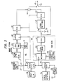
- Fig. 2 illustrates an embodiment of the signal generator (identified by 11 in Fig. 1) of the present invention.
- a frequency converter 22 is provided via a terminal 21 with a clock signal in synchronism with the data input to the FFT analyzer 17 in Fig. 1, that is, a fundamental clock signal from which are made the sample clock signals in the AID converters 13 and 14 and which is higher in frequency than these sample clock signals.
- the frequency converter 22 is formed by a phase lock loop or what is called PLL, and it converts the input clock signal into a clock signal which is synchronized therewith and has a frequency, for example, four times higher than the frequency of the input clock signal.
- the frequency converter 22 removes from the input clock signal jitter which was applied thereto, for instance, on the transmission line before it is provided to the terminal 21.
- the thus frequency-converted clock signal is frequency-divided by a frequency divider 23 corresponding to a set value of a frequency range setter 24.
- the set value of the frequency range setter 24 is altered in accordance with a change in the sampling frequency of a sampling circuit for generating time series samples in the fast Fourier transformer 15 (in Fig. 1).
- the output frequency of the frequency divider 23 is a predetermined integral multiple, for example, four times, of the sampling frequency of the A/D converters 13 and 14.
- the output of the frequency divider 23 is further frequency-divided by a frequency divider 25.
- the frequency dividing ratio of the frequency divider 25 is set to 1/k in accordance with a zooming factor k set by a zooming factor setter 26.
- a magnification coefficient for magnifying a certain frequency band for analysis by the FFT analyzer is the zooming factor k, which is an integer equal to or larger than 1 and, in the case of no magnification, the zooming factor .k is 1.
- the output of the frequency divider 25 is supplied via a changeover switch 27 to a clock terminal of an address counter 28.
- a waveform memory 29 is read out using the count value of the address counter 28.
- the waveform memory 29 has prestored therein sample values at equally spaced sample points of a composite waveform having a plurality of spectra. Accordingly, by successively reading out the sample values, the composite waveform is obtained in a digital form.
- the waveform memory 29 has prestored therein a plurality of waveforms as required, and the waveforms are selectively read out in accordance with the setting of a selector 31; namely, the area of the memory 29 to be read out is selected by the setting of the selector 31.
- Data of a weighted multiple sine wave to be stored in the waveform memory 29 is such as follows:
- the value of f(t), which is obtained by substituting each integer from 0 to N for t, is the sample value at each of N sample points of the multiple sine wave.
- ⁇ is - ⁇ i ⁇ and is a minimum one of values which give maximum instantaneous values of the ith term of f(t); and is the weight function.
- a frequency sweep signal waveform may also be stored in the waveform memory 29 as follows: Letting a sweep start angular frequency and a sweep end angular frequency be represented by w, and w s , respectively, where Each value of f(t), which is obtained by substituting each integer from 0 to N for t in the above expression (4), is the sample value at each of N sample points representing the sweep signal waveform.
- N is selected, for example, to an integral multiple more than 1 of 1024, for instance, four times, i.e. 4096.
- the abovesaid angular frequencies are selected as follows:
- the address counter 28 When having read out from the waveform memory 29 all sample values of one waveform, that is, when having counted N, the address counter 28 reaches its full count and then counts again from zero.
- the output read out from the waveform memory 29 is latched by a latch circuit 32 in synchronism with the output clock signal of the frequency divider 25, and the output of the latch circuit 32 is converted by a D/A converter 33 into an analog signal.
- the D/A converter 33 is a digital-analog multiplier which produces an analog signal obtained by multiplying digital and analog values, and which is supplied at its digital input terminal with the output digital value of the latch circuit 32 and at its reference power source terminal with an analog signal.
- To the reference power source terminal are selectively applied by a switch 34 a fixed DC analog value from a power source 35 and the output sine-wave signal from a sine-wave signal generator 36.
- the digital waveform signal from the latch circuit 32 is frequency-converted by the sine-wave signal.
- the sine-wave signal generator 36 is supplied at a clock terminal of an accumulator 37, for example, with the output of the frequency divider 23. Upon each application of the clock to the accumulator 37, the set value of a center frequency setter 38 is accumulated. A sine-wave memory 39 is read out using the accumulated value as an address therefor.
- the sine-wave memory 39 has stored therein a sinusoidal waveform in a digital form, and the signal read out therefrom is converted by a D/A converter 41 to an analog signal for output as the output signal of the sine-wave signal generator 36.
- a D/A converter 42 is provided for multiplying analog and digital signals to generate a correction signal.
- a digital value set in a correction setter 43 is multiplied by an analog value from the switch 34 for output in analog form.
- the multiplied outputs from the D/A converters 33 and 42 are added by an adder 44 and the added output is provided to an output terminal 45 of the signal generator 11.
- a random pulse generator 46 is provided for generating a random noise pulse signal as required and its output is selectively supplied via the switch 27 to the address counter 28.
- the random pulse generator 46 for example, as shown in Fig. 3, current is applied from a power source terminal 47 to such a noise source as a Zener diode 48 and the resulting thermal noise therein is amplified by an amplifier 49, the amplified output of which is filtered by a lowpass filter 51 to eliminate frequency components higher than a predetermined cutoff frequency, thereafter being provided to a non-inverting input terminal of a comparator 52.
- the level of the thermal noise is compared with a threshold level given by a DC voltage from a variable voltage source 53 to obtain random pulses from the comparator 52.
- the threshold voltage of the comparator 52 is adjustable by changing the output voltage of the variable voltage source 53.
- Fig. 2 the added output of the adder 44 and the output sine-wave signal of the sine-wave generator 36 are selectively supplied via a switch 54 to the output terminal 45 as required.
- the switch 27 is set to the side of the frequency divider 25 and the switch 34 set to the side of the power source 35.
- the address counter 28 is stepped by the output of the frequency divider 25 and, in consequence, each digital value of the selected waveform is read out from the waveform memory 29 and the converted output of the D/A converter 33 becomes an analog signal of the selected waveform. That is, there is derived at the output terminal 45 an analog signal of the composite waveform of only the spectra desired to analyze.
- a composite signal In the case of providing such a composite signal to a device under test for analysis, it contains only those frequency components which are known and expected to be obtained in the fast Fourier transformation, so that no errors are caused by other unnecessary frequency components; therefore, high precision analysis can be achieved.
- the value k of the zooming factor setter 26 is set to a value corresponding to the magnification coefficient at the FFT analyzer and, at the same time, the center frequency of the frequency range is set in the center frequency setter 38 and the sine-wave output is obtained from the sine-wave signal generator 36 and provided via the switch 34 to the D/A converters 33 and 42.
- the waveform signal read out from the waveform memory 29 in the same manner as described previously comprises spectra of compressed frequency intervals (i.e.
- the D/A converter 42 sets the DC level in the case of producing a signal within a certain frequency range from zero, and outputs a corrective value of the level of the center frequency in the case of producing a signal within a frequency range exclusive of zero. That is, in the output obtained by multiplying the output of the waveform memory 29 and the sine-wave signal, the frequency component of the sine-wave signal is lower in level than the other frequency components, and hence this level different is corrected.
- the switch 27 is connected to the side of the random pulse generator 46.
- the address counter 28 is incremented at random intervals, by which a random waveform signal can be generated from the waveform memory 29.
- the amplitude probability density distribution of the generated random waveform signal is substantially the same as that of the waveform in the memory which has been accessed.
- the waveform memory 29 are prestored waveforms of various functions having desired amplitude probability density distributions, such as Gaussian distribution, Poisson's distribution and the like, which are selectively designated by the waveform selector 31 to be accessed.
- the output of the waveform memory 29 becomes a random waveform signal having an amplitude probability density of Gaussian distribution.
- a random waveform signal having a desired amplitude probability density distribution it is possible to generate a random waveform signal having a desired amplitude probability density distribution.
- a single sine-wave signal can be yielded by connecting the switch 54 to the output side of the sine-wave generator 36.
- Fig. 4 While the embodiment of Fig. 2 is adapted so that the sine-wave signal is applied to the D/A converter 33 for multiplication, it is also possible to adopt such an arrangement, for instance, as shown in Fig. 4.
- the digital sine-wave signal is delivered from the sine-wave memory 39 in the sine-wave generator 36 and provided via a switch 56 to a digital multiplier 57, wherein it is multiplied by the digital waveform output from the latch circuit 32, and the multiplied output is applied to a digital adder 58.
- the digital sine-wave signal from the sine-wave memory 39 is supplied via the switch 56 to a correction signal generating digital multiplier 59, wherein it is multiplied by the set value of the correction setter 43.
- the multiplied output is provided to the adder 58, wherein it is added to the output of the multiplier 57 to correct the sine-wave signal component, and the added output is applied to the D/A converter 33.
- the signal generator operates in synchronism with the fundamental clock (the data input) of the FFT analyzer and provides an analog signal which has only a plurality of spectra to be analyzed, and hence it permits the reduction of an analysis error.
- the fundamental clock the data input
- measurement is repeated hundreds to thousands of times and the measured results are averaged for raising the accuracy of analysis.
- the present invention in the case of using, for example, the aforesaid weighted multiple sine wave, substantially the same measurement accuracy can be obtained with one measurement; namely, high precision measurement can be achieved in a short time.
- the present invention it is possible to obtain a plurality of spectra within a certain frequency range as required.
- the spectrum of the output analog signal can be brought into agreement with the spectrum to be analyzed.
- the use of a periodic signal may sometimes cause a measurement error but this can be avoided through the use of the thermal noise generator 46.
- By preparing a combination of preferred waveforms in accordance with various devices to be tested, that is, a plurality of preferred spectra for example, by prestoring sweep signal waveforms, multiple sinewaves, weighted multiple sine waves or the like in the waveform memory 29, these waveforms can selectively be output in accordance with a particular device to be tested.
- a signal of double spectral density can easily be obtained by multiplying the output of the waveform memory 29 by a sine-wave signal.
- spectra within a desired frequency range centering about an arbitrary frequency can be obtained.
- any waveform is read out from the waveform memory having prestored it, a signal of excellent spectral flatness can be obtained by preselecting the waveform.
- the readout period (the spectral density) by the random pulses can be optimized for the FFT analyzer and the output signal is not directly affected by the temperature of the thermal noise.
- the precision of the level of the DC component can be raised.
- the level of the center frequency of the output signal can be corrected in the case of multiplying the output of the waveform memory 29 by the sine-wave signal.
Landscapes
- Physics & Mathematics (AREA)
- Mathematical Physics (AREA)
- General Physics & Mathematics (AREA)
- Analogue/Digital Conversion (AREA)
- Measurement Of Resistance Or Impedance (AREA)
- Complex Calculations (AREA)
Claims (12)
Applications Claiming Priority (2)
| Application Number | Priority Date | Filing Date | Title |
|---|---|---|---|
| JP167370/82 | 1982-09-24 | ||
| JP57167370A JPS5955523A (ja) | 1982-09-24 | 1982-09-24 | デジタルスペクトルアナライザ用信号発生器 |
Publications (3)
| Publication Number | Publication Date |
|---|---|
| EP0107050A2 EP0107050A2 (fr) | 1984-05-02 |
| EP0107050A3 EP0107050A3 (en) | 1984-09-12 |
| EP0107050B1 true EP0107050B1 (fr) | 1987-03-11 |
Family
ID=15848448
Family Applications (1)
| Application Number | Title | Priority Date | Filing Date |
|---|---|---|---|
| EP83109461A Expired EP0107050B1 (fr) | 1982-09-24 | 1983-09-22 | Générateur de signaux pour un analyseur de spectre digital |
Country Status (4)
| Country | Link |
|---|---|
| US (1) | US4539518A (fr) |
| EP (1) | EP0107050B1 (fr) |
| JP (1) | JPS5955523A (fr) |
| DE (1) | DE3370210D1 (fr) |
Families Citing this family (28)
| Publication number | Priority date | Publication date | Assignee | Title |
|---|---|---|---|---|
| JPS6071966A (ja) * | 1983-09-28 | 1985-04-23 | Advantest Corp | デジタルスペクトルアナライザ |
| US4689562A (en) * | 1983-10-11 | 1987-08-25 | Elscint Ltd. | NMR Imaging method and system |
| JPS6140629A (ja) * | 1984-07-31 | 1986-02-26 | Reikouon Denki Kk | 定出力超低周波関数信号発生器 |
| JPH0640114B2 (ja) * | 1984-11-09 | 1994-05-25 | 株式会社アドバンテスト | 信号発生装置 |
| US4744041A (en) * | 1985-03-04 | 1988-05-10 | International Business Machines Corporation | Method for testing DC motors |
| US4677674A (en) * | 1985-04-03 | 1987-06-30 | Seth Snyder | Apparatus and method for reestablishing previously established settings on the controls of an audio mixer |
| EP0276332A1 (fr) * | 1986-12-30 | 1988-08-03 | S.A. Acec Transport | Procédé et dispositif pour décoder un signal-code |
| JP2575754B2 (ja) * | 1987-11-20 | 1997-01-29 | 株式会社アドバンテスト | 周波数応答関数測定法 |
| JPH03296308A (ja) * | 1990-04-13 | 1991-12-27 | Advantest Corp | 波形発生器 |
| US5262957A (en) * | 1990-11-09 | 1993-11-16 | Global Communications, Inc. | Inexpensive portable RF spectrum analyzer with calibration features |
| US5784002A (en) * | 1995-05-02 | 1998-07-21 | Mobile Telecommunication Technologies | Low-power random digit generator |
| DE19650839C2 (de) * | 1996-11-29 | 2000-06-08 | Tektronix Inc | Durchgangsmodulator zum Verjittern von Signalen |
| US6725108B1 (en) | 1999-01-28 | 2004-04-20 | International Business Machines Corporation | System and method for interpretation and visualization of acoustic spectra, particularly to discover the pitch and timbre of musical sounds |
| DE60038672T2 (de) * | 1999-12-24 | 2009-05-28 | Anritsu Corp. | Wandergenerator und diesen enthaltender digitaler leitungsprüfer |
| DE10038865A1 (de) * | 2000-08-04 | 2002-02-14 | Sz Testsysteme Ag | Kalibrierverfahren |
| US7016805B2 (en) * | 2001-12-14 | 2006-03-21 | Wavecrest Corporation | Method and apparatus for analyzing a distribution |
| JP2008000447A (ja) * | 2006-06-23 | 2008-01-10 | Kenzo Kase | 身体用叩打具 |
| US8229754B1 (en) * | 2006-10-23 | 2012-07-24 | Adobe Systems Incorporated | Selecting features of displayed audio data across time |
| US8140292B2 (en) * | 2007-09-18 | 2012-03-20 | Wisconsin Alumni Research Foundation | Method and system for controlling a voltage waveform |
| US8642874B2 (en) * | 2010-01-22 | 2014-02-04 | Overtone Labs, Inc. | Drum and drum-set tuner |
| JP5179615B2 (ja) * | 2011-03-29 | 2013-04-10 | アンリツ株式会社 | Apd測定器の検査装置及び検査方法 |
| RU2477153C2 (ru) * | 2011-05-31 | 2013-03-10 | Государственное образовательное учреждение высшего профессионального образования "Волгоградский государственный медицинский университет" Министерства здравоохранения и социального развития Российской Федерации | Способ профилактики развития острого послеоперационного панкреатита при эндоскопических транспапиллярных вмешательствах |
| EE05668B1 (et) * | 2011-08-30 | 2013-08-15 | Tallinna Tehnika�likool | Meetod ja seade ssteemide ja substantside laiaribaliseks analsimiseks |
| WO2013082250A1 (fr) | 2011-11-30 | 2013-06-06 | Overtone Labs, Inc. | Accordeur de fûts de batterie et de batterie |
| US9153221B2 (en) | 2012-09-11 | 2015-10-06 | Overtone Labs, Inc. | Timpani tuning and pitch control system |
| CN105181117B (zh) * | 2015-09-10 | 2018-07-17 | 西安翔迅科技有限责任公司 | 程控电荷型振动传感器仿真信号源 |
| US11131704B2 (en) * | 2019-03-26 | 2021-09-28 | Rohde & Schwarz Gmbh & Co. Kg | Method and measuring apparatus for testing a device under test |
| CN112560771B (zh) * | 2020-12-25 | 2024-01-23 | 北京航天测控技术有限公司 | 一种带宽特征曲线的拟合系统、方法和装置 |
Family Cites Families (17)
| Publication number | Priority date | Publication date | Assignee | Title |
|---|---|---|---|---|
| US3566035A (en) * | 1969-07-17 | 1971-02-23 | Bell Telephone Labor Inc | Real time cepstrum analyzer |
| US3745317A (en) * | 1970-05-04 | 1973-07-10 | Commissariat Energie Atomique | System for generating the fourier transform of a function |
| FR2147770B1 (fr) * | 1971-04-27 | 1974-06-21 | Thomson Csf | |
| JPS5624226B2 (fr) * | 1974-04-23 | 1981-06-04 | ||
| JPS5827546B2 (ja) * | 1975-04-22 | 1983-06-10 | 日本電気株式会社 | エンザンソウチ |
| DE2553705B1 (de) * | 1975-11-28 | 1977-03-31 | Siemens Ag | Schaltungsanordnung zur frequenzselektiven auswertung der amplituden eines oder mehrerer signale |
| US4067060A (en) * | 1976-07-06 | 1978-01-03 | Canadian Patents And Development Limited | Transfer function measurement |
| JPS5336154A (en) * | 1976-09-16 | 1978-04-04 | Kokusai Denshin Denwa Co Ltd | Method of reading out digital function generator |
| US4093988A (en) * | 1976-11-08 | 1978-06-06 | General Electric Company | High speed frequency response measurement |
| FR2448722A1 (fr) * | 1979-02-09 | 1980-09-05 | Enertec | Procedes et appareils pour l'analyse de formes d'ondes periodiques |
| US4243935A (en) * | 1979-05-18 | 1981-01-06 | The United States Of America As Represented By The Secretary Of The Navy | Adaptive detector |
| US4296374A (en) * | 1979-10-11 | 1981-10-20 | Bell Telephone Laboratories, Incorporated | Wideband digital spectrometer |
| US4327419A (en) * | 1980-02-22 | 1982-04-27 | Kawai Musical Instrument Mfg. Co., Ltd. | Digital noise generator for electronic musical instruments |
| US4321680A (en) * | 1980-04-22 | 1982-03-23 | Wavetek Rockland Inc. | Spectrum analyzer with frequency band selection |
| JPS6014368B2 (ja) * | 1980-07-28 | 1985-04-12 | 株式会社 ナムコ | 任意波形発生回路 |
| US4408284A (en) * | 1981-01-19 | 1983-10-04 | The United States Of America As Represented By The Secretary Of The Navy | Signal processing system |
| BE892242A (fr) * | 1982-02-23 | 1982-06-16 | Dev Et D Industrialisation Des | Generateur numerique programmable. |
-
1982
- 1982-09-24 JP JP57167370A patent/JPS5955523A/ja active Granted
-
1983
- 1983-09-19 US US06/533,780 patent/US4539518A/en not_active Expired - Lifetime
- 1983-09-22 DE DE8383109461T patent/DE3370210D1/de not_active Expired
- 1983-09-22 EP EP83109461A patent/EP0107050B1/fr not_active Expired
Also Published As
| Publication number | Publication date |
|---|---|
| EP0107050A3 (en) | 1984-09-12 |
| EP0107050A2 (fr) | 1984-05-02 |
| JPH0350224B2 (fr) | 1991-08-01 |
| DE3370210D1 (en) | 1987-04-16 |
| JPS5955523A (ja) | 1984-03-30 |
| US4539518A (en) | 1985-09-03 |
Similar Documents
| Publication | Publication Date | Title |
|---|---|---|
| EP0107050B1 (fr) | Générateur de signaux pour un analyseur de spectre digital | |
| Hidalgo et al. | A simple adjustable window algorithm to improve FFT measurements | |
| Peetz | Dynamic testing of waveform recorders | |
| US4067060A (en) | Transfer function measurement | |
| US4264959A (en) | Testing procedure and circuit for the determination of frequency distortions and group delay time distortion of a test object | |
| US4647873A (en) | Adaptive linear FM sweep corrective system | |
| EP1085329A2 (fr) | Procédé d'horodatage du flanc de front d'ondes d'un signal d'entrée | |
| Dallet et al. | Dynamic characterisation of analogue-to-digital converters | |
| Gans | Dynamic calibration of waveform recorders and oscilloscopes using pulse standards | |
| US6522983B1 (en) | Timebase calibration method for an equivalent time sampling digitizing instrument | |
| US4947130A (en) | Impedance measuring apparatus | |
| US20020075951A1 (en) | Method and apparatus to measure jitter | |
| Tilden et al. | Overview of IEEE-STD-1241" standard for terminology and test methods for analog-to-digital converters" | |
| WO2000013032A1 (fr) | Procede et appareil de mesure des fonctions de transfert a faible puissance/largeur de bande | |
| US4237422A (en) | Chromatograph signal generator | |
| US5933013A (en) | Calibration circuit for calibrating frequency characteristics of an AC/DC converter | |
| US5008845A (en) | Method and apparatus for generating a chirp signal | |
| EP0191478A2 (fr) | Circuit de mesure pour l'évaluation d'un convertisseur numérique-analogique | |
| EP0391524B1 (fr) | Générateur de fréquences multiples à accumulation de phase | |
| JP2867769B2 (ja) | 音響測定方法およびその装置 | |
| GB2036985A (en) | Method and apparatus for determining the transmission properties of a signal path | |
| US4860227A (en) | Circuit for measuring characteristics of a device under test | |
| EP0430256B1 (fr) | Procédé et dispositif pour calibrer le niveau des signeaux de sortie pour des appareils d'analyse d'ondes | |
| US4264859A (en) | Method and apparatus for measurement of attenuation and distortion by a test object | |
| GB2023852A (en) | Method of and circuit arrangement for measuring characteritics of information tansmission systems |
Legal Events
| Date | Code | Title | Description |
|---|---|---|---|
| PUAI | Public reference made under article 153(3) epc to a published international application that has entered the european phase |
Free format text: ORIGINAL CODE: 0009012 |
|
| 17P | Request for examination filed |
Effective date: 19830922 |
|
| AK | Designated contracting states |
Designated state(s): DE GB NL |
|
| PUAL | Search report despatched |
Free format text: ORIGINAL CODE: 0009013 |
|
| AK | Designated contracting states |
Designated state(s): DE GB NL |
|
| GRAA | (expected) grant |
Free format text: ORIGINAL CODE: 0009210 |
|
| AK | Designated contracting states |
Kind code of ref document: B1 Designated state(s): DE GB NL |
|
| REF | Corresponds to: |
Ref document number: 3370210 Country of ref document: DE Date of ref document: 19870416 |
|
| PLBE | No opposition filed within time limit |
Free format text: ORIGINAL CODE: 0009261 |
|
| STAA | Information on the status of an ep patent application or granted ep patent |
Free format text: STATUS: NO OPPOSITION FILED WITHIN TIME LIMIT |
|
| 26N | No opposition filed | ||
| PGFP | Annual fee paid to national office [announced via postgrant information from national office to epo] |
Ref country code: GB Payment date: 19930914 Year of fee payment: 11 |
|
| PGFP | Annual fee paid to national office [announced via postgrant information from national office to epo] |
Ref country code: NL Payment date: 19930930 Year of fee payment: 11 Ref country code: DE Payment date: 19930930 Year of fee payment: 11 |
|
| PG25 | Lapsed in a contracting state [announced via postgrant information from national office to epo] |
Ref country code: GB Effective date: 19940922 |
|
| PG25 | Lapsed in a contracting state [announced via postgrant information from national office to epo] |
Ref country code: NL Effective date: 19950401 |
|
| NLV4 | Nl: lapsed or anulled due to non-payment of the annual fee | ||
| GBPC | Gb: european patent ceased through non-payment of renewal fee |
Effective date: 19940922 |
|
| PG25 | Lapsed in a contracting state [announced via postgrant information from national office to epo] |
Ref country code: DE Effective date: 19950601 |