EP0105083B1 - Module plat - Google Patents
Module plat Download PDFInfo
- Publication number
- EP0105083B1 EP0105083B1 EP83104867A EP83104867A EP0105083B1 EP 0105083 B1 EP0105083 B1 EP 0105083B1 EP 83104867 A EP83104867 A EP 83104867A EP 83104867 A EP83104867 A EP 83104867A EP 0105083 B1 EP0105083 B1 EP 0105083B1
- Authority
- EP
- European Patent Office
- Prior art keywords
- circuit board
- contact
- printed circuit
- flat assembly
- component
- Prior art date
- Legal status (The legal status is an assumption and is not a legal conclusion. Google has not performed a legal analysis and makes no representation as to the accuracy of the status listed.)
- Expired
Links
- 238000001816 cooling Methods 0.000 claims abstract description 6
- 239000004020 conductor Substances 0.000 description 5
- 230000006835 compression Effects 0.000 description 2
- 238000007906 compression Methods 0.000 description 2
- 238000003780 insertion Methods 0.000 description 2
- 230000037431 insertion Effects 0.000 description 2
- 238000000034 method Methods 0.000 description 2
- 238000011161 development Methods 0.000 description 1
- 230000018109 developmental process Effects 0.000 description 1
- 239000000463 material Substances 0.000 description 1
- 239000002184 metal Substances 0.000 description 1
- 238000012856 packing Methods 0.000 description 1
- 238000012545 processing Methods 0.000 description 1
- 229910000679 solder Inorganic materials 0.000 description 1
- 230000003068 static effect Effects 0.000 description 1
Images
Classifications
-
- H—ELECTRICITY
- H05—ELECTRIC TECHNIQUES NOT OTHERWISE PROVIDED FOR
- H05K—PRINTED CIRCUITS; CASINGS OR CONSTRUCTIONAL DETAILS OF ELECTRIC APPARATUS; MANUFACTURE OF ASSEMBLAGES OF ELECTRICAL COMPONENTS
- H05K7/00—Constructional details common to different types of electric apparatus
- H05K7/20—Modifications to facilitate cooling, ventilating, or heating
- H05K7/2039—Modifications to facilitate cooling, ventilating, or heating characterised by the heat transfer by conduction from the heat generating element to a dissipating body
-
- H—ELECTRICITY
- H01—ELECTRIC ELEMENTS
- H01R—ELECTRICALLY-CONDUCTIVE CONNECTIONS; STRUCTURAL ASSOCIATIONS OF A PLURALITY OF MUTUALLY-INSULATED ELECTRICAL CONNECTING ELEMENTS; COUPLING DEVICES; CURRENT COLLECTORS
- H01R12/00—Structural associations of a plurality of mutually-insulated electrical connecting elements, specially adapted for printed circuits, e.g. printed circuit boards [PCB], flat or ribbon cables, or like generally planar structures, e.g. terminal strips, terminal blocks; Coupling devices specially adapted for printed circuits, flat or ribbon cables, or like generally planar structures; Terminals specially adapted for contact with, or insertion into, printed circuits, flat or ribbon cables, or like generally planar structures
- H01R12/70—Coupling devices
- H01R12/71—Coupling devices for rigid printing circuits or like structures
- H01R12/712—Coupling devices for rigid printing circuits or like structures co-operating with the surface of the printed circuit or with a coupling device exclusively provided on the surface of the printed circuit
- H01R12/714—Coupling devices for rigid printing circuits or like structures co-operating with the surface of the printed circuit or with a coupling device exclusively provided on the surface of the printed circuit with contacts abutting directly the printed circuit; Button contacts therefore provided on the printed circuit
-
- H—ELECTRICITY
- H05—ELECTRIC TECHNIQUES NOT OTHERWISE PROVIDED FOR
- H05K—PRINTED CIRCUITS; CASINGS OR CONSTRUCTIONAL DETAILS OF ELECTRIC APPARATUS; MANUFACTURE OF ASSEMBLAGES OF ELECTRICAL COMPONENTS
- H05K7/00—Constructional details common to different types of electric apparatus
- H05K7/02—Arrangements of circuit components or wiring on supporting structure
- H05K7/10—Plug-in assemblages of components, e.g. IC sockets
- H05K7/1015—Plug-in assemblages of components, e.g. IC sockets having exterior leads
- H05K7/103—Plug-in assemblages of components, e.g. IC sockets having exterior leads co-operating by sliding, e.g. DIP carriers
- H05K7/1038—Plug-in assemblages of components, e.g. IC sockets having exterior leads co-operating by sliding, e.g. DIP carriers with spring contact pieces
-
- H—ELECTRICITY
- H05—ELECTRIC TECHNIQUES NOT OTHERWISE PROVIDED FOR
- H05K—PRINTED CIRCUITS; CASINGS OR CONSTRUCTIONAL DETAILS OF ELECTRIC APPARATUS; MANUFACTURE OF ASSEMBLAGES OF ELECTRICAL COMPONENTS
- H05K7/00—Constructional details common to different types of electric apparatus
- H05K7/02—Arrangements of circuit components or wiring on supporting structure
- H05K7/10—Plug-in assemblages of components, e.g. IC sockets
- H05K7/1053—Plug-in assemblages of components, e.g. IC sockets having interior leads
- H05K7/1076—Plug-in assemblages of components, e.g. IC sockets having interior leads co-operating by sliding
-
- H—ELECTRICITY
- H01—ELECTRIC ELEMENTS
- H01R—ELECTRICALLY-CONDUCTIVE CONNECTIONS; STRUCTURAL ASSOCIATIONS OF A PLURALITY OF MUTUALLY-INSULATED ELECTRICAL CONNECTING ELEMENTS; COUPLING DEVICES; CURRENT COLLECTORS
- H01R31/00—Coupling parts supported only by co-operation with counterpart
Definitions
- the invention relates to a flat module, consisting of a printed circuit board equipped with electrical components, a connector part with a plurality of contact elements and a pressure component exerting pressure on a printed circuit board surface, for example a cooling device.
- the aim is to keep signal lines as short as possible with a defined characteristic impedance and thus achieve high switching speeds.
- This can be achieved with the aid of printed circuit boards which have single or multi-layer printed circuit boards with integrated components and which are connected to a wiring board via electrical connectors.
- this is also constructed in several layers and contains signal lines for connecting modules to one another, but also potential and supply lines.
- the numerous external connections required for this are distributed in a very confined space on the underside in order to establish the connection to the circuit board without detours.
- the invention was therefore based on the object of designing a flat module of the type mentioned above provided with a connector part in such a way that error sources resulting from plugging and unplugging operations are reduced.
- This object is achieved in that on the side of the printed circuit board opposite the pressure contacting surfaces are arranged evenly distributed, that the connector part extends over this entire side surface, and that it has openings for the contact elements above the contact surfaces, each consisting of a spring shaft and consist of a connecting lug designed as a compression spring, which rests under spring tension on the contacting surfaces. In this way, no one-sided pressure forces act on the circuit board, so that no deflection occurs.
- the back pressure on the circuit board can be preset by the choice of the spring constant of the connection lugs.
- the contact elements are not rigidly connected to the printed circuit board, the forces that occur during insertion and removal do not lead to deflection of the printed circuit board. This prevents cracks and breaks in conductor tracks or in soldered connections that result from static or dynamic forces.
- the terminal lugs are designed as curved leaf springs. If the connecting lugs are firmly connected to the contacting surfaces, the contact security is increased, which can be further improved in that the spring shafts each consist of three U-shaped side parts which form a receiving channel for a contact pin, and that at least one of the U- Leg has a resilient portion for pressing against the contact pin.
- the spring shafts of the contact elements are advantageously fixed in each case by a snap lock in the openings of the connector part. If the dimensions of the terminal lugs are such that the entire contact element can be plugged into a breakthrough, then an assignment of connecting elements and of connecting surfaces for different printed circuit boards can optionally be made.
- the circuit board is fitted into a first recess of the connector part and the pressure component into a second recess parallel to the circuit board in the connector part.
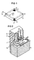
- the flat module is determined in its outer shape by a plate-like connector part 3, which has a first and a second, opening to one of the flat sides recess 1, 14 for receiving a circuit board 7 or one is provided with screw connections 17 attached pressure component 4.
- This can consist, for example, of a metal plate which serves as a cooling device for the heat-emitting components of the printed circuit board.
- the connector part 3 has in its base 6 in the area of the first recess 1 a plurality of grid-like, rectangular openings 2 for contact elements 9, 18, and forms with the collar created by the recess 1, 14 an enclosure of the printed circuit board.
- FIG. 2 shows a cross section through the flat module along the dash-dotted line 11 in FIG. 1.
- a contact element 9, 18, consisting of a spring shaft 18 and a connecting lug 9 designed as a compression spring, is fixed with a snap lock.
- the spring shaft 18 comprises three side parts which are connected to one another in a U-shape and form a receiving channel for a contact pin (not shown), the two U-legs having curved, resilient central sections which constrict the receiving channel in a funnel shape.
- you create a contact pin you create a double contact.
- the U-legs sit on the first lugs 12 in front of the inner openings of the openings 2.
- a tongue 11 directed towards the outer opening of the openings 2 spreads out from the spring shaft 18 and engages behind a second lug 10 in the opening 2.
- the connecting lug 9 consists of a curved leaf spring, the radius of curvature and leaf width of which are dimensioned such that the entire contact element 9, 18 can be inserted into an opening 2.
- the sheet is therefore not wider than the opening 2, and the curvature diameter corresponds approximately to the length of the opening 2, it should be borne in mind that the curvature diameter can decrease under pressure.
- the free end of the leaf spring protrudes into the first recess 1 and generates a spring pressure acting vertically on the circuit board 7 which is precisely fitted therein with respect to the side edges.
- a pressure is exerted on the building blocks 5 via the pressure component 4, for example in order to produce good thermal contact, which is transmitted to the printed circuit board 7 and would lead to a deflection if it were not canceled by the spring pressure of the connecting lugs.
- a sufficient and uniform force between the connecting lugs 9 and the contacting surfaces 8 is achieved in that the connecting lugs 9 are overstretched before assembly.
- the terminal lugs 9 and the contact elements 9, 18 are distributed so that a uniform surface pressure is generated on the circuit board 7.
- an elastic connection between the connector part 3 and the circuit board 7 is produced in this way.
Landscapes
- Engineering & Computer Science (AREA)
- Microelectronics & Electronic Packaging (AREA)
- Physics & Mathematics (AREA)
- Thermal Sciences (AREA)
- Coupling Device And Connection With Printed Circuit (AREA)
- Led Device Packages (AREA)
Claims (9)
Priority Applications (1)
| Application Number | Priority Date | Filing Date | Title |
|---|---|---|---|
| AT83104867T ATE26519T1 (de) | 1982-09-30 | 1983-05-17 | Flachbaugruppe. |
Applications Claiming Priority (2)
| Application Number | Priority Date | Filing Date | Title |
|---|---|---|---|
| DE3236325 | 1982-09-30 | ||
| DE19823236325 DE3236325A1 (de) | 1982-09-30 | 1982-09-30 | Flachbaugruppe |
Publications (3)
| Publication Number | Publication Date |
|---|---|
| EP0105083A2 EP0105083A2 (fr) | 1984-04-11 |
| EP0105083A3 EP0105083A3 (en) | 1984-12-12 |
| EP0105083B1 true EP0105083B1 (fr) | 1987-04-08 |
Family
ID=6174642
Family Applications (1)
| Application Number | Title | Priority Date | Filing Date |
|---|---|---|---|
| EP83104867A Expired EP0105083B1 (fr) | 1982-09-30 | 1983-05-17 | Module plat |
Country Status (5)
| Country | Link |
|---|---|
| US (1) | US4516188A (fr) |
| EP (1) | EP0105083B1 (fr) |
| JP (1) | JPS5966079A (fr) |
| AT (1) | ATE26519T1 (fr) |
| DE (2) | DE3236325A1 (fr) |
Families Citing this family (8)
| Publication number | Priority date | Publication date | Assignee | Title |
|---|---|---|---|---|
| JPS6093777A (ja) * | 1983-09-30 | 1985-05-25 | シーメンス、アクチエンゲゼルシヤフト | プリント配線板アセンブリ |
| US4693528A (en) * | 1985-05-31 | 1987-09-15 | Amp Incorporated | Surface mount connector with floating terminals |
| FR2606559B1 (fr) * | 1986-11-12 | 1990-03-02 | Rech Digitales Sarl Et | Connecteur modulaire |
| FR2638293B1 (fr) * | 1988-10-26 | 1991-01-18 | Itt Composants Instr | Connecteur electrique pour cartes a memoire electronique, procede de realisation d'un tel connecteur et dispositif de lecture-ecriture integrant un tel connecteur |
| US4975067A (en) * | 1989-09-27 | 1990-12-04 | Elsag International B.V. | Surface contact power connector |
| WO1991015101A1 (fr) * | 1990-03-17 | 1991-10-03 | Amphenol-Tuchel Electronics Gmbh | Dispositif de contact, en particulier pour un sim |
| US5641314A (en) * | 1995-06-30 | 1997-06-24 | The Whitaker Corporation | Memory card receptacle connector and contact terminal |
| DE19724664B4 (de) * | 1997-06-11 | 2008-01-03 | Lisa Dräxlmaier GmbH | Einbauteil mit speziellem elektrischen Kontaktierungssystem |
Family Cites Families (12)
| Publication number | Priority date | Publication date | Assignee | Title |
|---|---|---|---|---|
| US2779007A (en) * | 1951-12-21 | 1957-01-22 | Ibm | Plugboard contactor |
| US3539965A (en) * | 1968-06-28 | 1970-11-10 | Dale Electronics | Socket connector assembly |
| IL40587A (en) * | 1971-11-05 | 1975-04-25 | Bunker Ramo | Electrical connector assemblies |
| US3873173A (en) * | 1973-10-05 | 1975-03-25 | Itt | Electrical connector assembly |
| US4045105A (en) * | 1974-09-23 | 1977-08-30 | Advanced Memory Systems, Inc. | Interconnected leadless package receptacle |
| US3993123A (en) * | 1975-10-28 | 1976-11-23 | International Business Machines Corporation | Gas encapsulated cooling module |
| US4089575A (en) * | 1976-09-27 | 1978-05-16 | Amp Incorporated | Connector for connecting a circuit element to the surface of a substrate |
| FR2378423A1 (fr) * | 1977-01-25 | 1978-08-18 | Amp Inc | Connecteur electrique de montage de substrats pour circuits integres sur des plaquettes a circuit imprime |
| JPS5533653U (fr) * | 1978-08-24 | 1980-03-04 | ||
| US4277816A (en) * | 1979-05-29 | 1981-07-07 | International Business Machines Corporation | Electronic circuit module cooling |
| US4330163A (en) * | 1979-12-05 | 1982-05-18 | E. I. Du Pont De Nemours And Company | Zero insertion force connector for LSI circuit package |
| US4346952A (en) * | 1980-06-16 | 1982-08-31 | Amp Incorporated | Connector for a ceramic substrate |
-
1982
- 1982-09-30 DE DE19823236325 patent/DE3236325A1/de not_active Ceased
-
1983
- 1983-05-17 EP EP83104867A patent/EP0105083B1/fr not_active Expired
- 1983-05-17 DE DE8383104867T patent/DE3370927D1/de not_active Expired
- 1983-05-17 AT AT83104867T patent/ATE26519T1/de not_active IP Right Cessation
- 1983-06-21 JP JP58111767A patent/JPS5966079A/ja active Pending
- 1983-08-25 US US06/526,371 patent/US4516188A/en not_active Expired - Fee Related
Also Published As
| Publication number | Publication date |
|---|---|
| DE3236325A1 (de) | 1984-04-05 |
| DE3370927D1 (en) | 1987-05-14 |
| ATE26519T1 (de) | 1987-04-15 |
| EP0105083A3 (en) | 1984-12-12 |
| US4516188A (en) | 1985-05-07 |
| EP0105083A2 (fr) | 1984-04-11 |
| JPS5966079A (ja) | 1984-04-14 |
Similar Documents
| Publication | Publication Date | Title |
|---|---|---|
| DE69609183T2 (de) | Oberflächenmontierbarer elektrischer verbinder | |
| DE3790062C2 (fr) | ||
| DE68915973T2 (de) | Elektrischer Verbinder unter Verwendung einer Leiterplatte. | |
| EP1536525B1 (fr) | Dipositif pour contacter une plaque de circuit au moyen d'un connecteur | |
| DE69900420T2 (de) | Rechtwinkliger Verbinder mit gleichmässig langen Signalwegen | |
| EP0092086B1 (fr) | Assemblage de connexion pour un dispositif électrique en forme de plaque | |
| DE3436119C2 (de) | Kontaktfederelement zum Kontaktieren von Leiterplatten | |
| EP0105083B1 (fr) | Module plat | |
| DE69006167T2 (de) | Verbesserte flächige Trägerstruktur für Leiterplatte. | |
| EP0153990B1 (fr) | Module plat | |
| EP1649549B1 (fr) | Module de connexion de conducteurs pour des cartes a circuits imprimes | |
| DE60022798T2 (de) | Elektrischer Verbindungsstecker mit wählbarer Kompatibilität | |
| EP0483532B1 (fr) | Dispositifs de connexion pour circuits imprimés | |
| DE1765989B2 (de) | Steckverbinder für die Aufnahme einer mit Kontaktflächen versehenen Druckschaltungskarte | |
| WO2001069729A1 (fr) | Connexion par enfichage | |
| EP1175712B1 (fr) | Connecteur enfichable pour cartes de circuits imprimes | |
| EP0402739B1 (fr) | Dispositif pour coupler électriquement des unités électriques enfichables | |
| EP0680117A2 (fr) | Connexion à fiche entre panneaux arrières et circuits imprimes | |
| EP1129511A1 (fr) | Composant electrique pour carte de circuits et procede pour implanter automatiquement des composants de ce type sur des cartes de circuits | |
| EP1168526A2 (fr) | Connecteur pour plaque à circuit intégré | |
| DE8227513U1 (de) | Flachbaugruppe | |
| DE2332556C2 (de) | Steckkontaktverbindung | |
| DE3335615A1 (de) | Flachbaugruppe | |
| DE2024563A1 (de) | Steckverbindung | |
| DE2855400B2 (de) | Aufbausystem für Geräte der elektrischen Nachrichtentechnik |
Legal Events
| Date | Code | Title | Description |
|---|---|---|---|
| PUAI | Public reference made under article 153(3) epc to a published international application that has entered the european phase |
Free format text: ORIGINAL CODE: 0009012 |
|
| AK | Designated contracting states |
Designated state(s): AT BE CH DE FR GB IT LI NL |
|
| PUAL | Search report despatched |
Free format text: ORIGINAL CODE: 0009013 |
|
| AK | Designated contracting states |
Designated state(s): AT BE CH DE FR GB IT LI NL |
|
| 17P | Request for examination filed |
Effective date: 19841221 |
|
| 17Q | First examination report despatched |
Effective date: 19860520 |
|
| GRAA | (expected) grant |
Free format text: ORIGINAL CODE: 0009210 |
|
| AK | Designated contracting states |
Kind code of ref document: B1 Designated state(s): AT BE CH DE FR GB IT LI NL |
|
| REF | Corresponds to: |
Ref document number: 26519 Country of ref document: AT Date of ref document: 19870415 Kind code of ref document: T |
|
| REF | Corresponds to: |
Ref document number: 3370927 Country of ref document: DE Date of ref document: 19870514 |
|
| ET | Fr: translation filed | ||
| ITF | It: translation for a ep patent filed | ||
| PLBE | No opposition filed within time limit |
Free format text: ORIGINAL CODE: 0009261 |
|
| STAA | Information on the status of an ep patent application or granted ep patent |
Free format text: STATUS: NO OPPOSITION FILED WITHIN TIME LIMIT |
|
| 26N | No opposition filed | ||
| PGFP | Annual fee paid to national office [announced via postgrant information from national office to epo] |
Ref country code: GB Payment date: 19890430 Year of fee payment: 7 |
|
| PGFP | Annual fee paid to national office [announced via postgrant information from national office to epo] |
Ref country code: AT Payment date: 19890503 Year of fee payment: 7 |
|
| PGFP | Annual fee paid to national office [announced via postgrant information from national office to epo] |
Ref country code: FR Payment date: 19890522 Year of fee payment: 7 |
|
| ITTA | It: last paid annual fee | ||
| PG25 | Lapsed in a contracting state [announced via postgrant information from national office to epo] |
Ref country code: LI Effective date: 19890531 Ref country code: CH Effective date: 19890531 |
|
| PGFP | Annual fee paid to national office [announced via postgrant information from national office to epo] |
Ref country code: NL Payment date: 19890531 Year of fee payment: 7 |
|
| PGFP | Annual fee paid to national office [announced via postgrant information from national office to epo] |
Ref country code: BE Payment date: 19890612 Year of fee payment: 7 |
|
| REG | Reference to a national code |
Ref country code: CH Ref legal event code: PL |
|
| PG25 | Lapsed in a contracting state [announced via postgrant information from national office to epo] |
Ref country code: DE Effective date: 19900201 |
|
| PG25 | Lapsed in a contracting state [announced via postgrant information from national office to epo] |
Ref country code: GB Effective date: 19900517 Ref country code: AT Effective date: 19900517 |
|
| PG25 | Lapsed in a contracting state [announced via postgrant information from national office to epo] |
Ref country code: BE Effective date: 19900531 |
|
| BERE | Be: lapsed |
Owner name: SIEMENS A.G. BERLIN UND MUNCHEN Effective date: 19900531 |
|
| PG25 | Lapsed in a contracting state [announced via postgrant information from national office to epo] |
Ref country code: NL Effective date: 19901201 |
|
| GBPC | Gb: european patent ceased through non-payment of renewal fee | ||
| NLV4 | Nl: lapsed or anulled due to non-payment of the annual fee | ||
| PG25 | Lapsed in a contracting state [announced via postgrant information from national office to epo] |
Ref country code: FR Effective date: 19910131 |
|
| REG | Reference to a national code |
Ref country code: FR Ref legal event code: ST |