EP0104852A2 - Tonfrequenzverstärker - Google Patents
Tonfrequenzverstärker Download PDFInfo
- Publication number
- EP0104852A2 EP0104852A2 EP83305472A EP83305472A EP0104852A2 EP 0104852 A2 EP0104852 A2 EP 0104852A2 EP 83305472 A EP83305472 A EP 83305472A EP 83305472 A EP83305472 A EP 83305472A EP 0104852 A2 EP0104852 A2 EP 0104852A2
- Authority
- EP
- European Patent Office
- Prior art keywords
- fet
- channel mos
- circuit
- voltage
- operational amplifier
- Prior art date
- Legal status (The legal status is an assumption and is not a legal conclusion. Google has not performed a legal analysis and makes no representation as to the accuracy of the status listed.)
- Ceased
Links
- 239000003990 capacitor Substances 0.000 claims description 13
- 230000005236 sound signal Effects 0.000 claims description 11
- 230000001105 regulatory effect Effects 0.000 claims description 10
- 230000003321 amplification Effects 0.000 claims description 6
- 238000003199 nucleic acid amplification method Methods 0.000 claims description 6
- 229910044991 metal oxide Inorganic materials 0.000 claims description 4
- 150000004706 metal oxides Chemical class 0.000 claims description 4
- 230000017525 heat dissipation Effects 0.000 description 4
- 230000007423 decrease Effects 0.000 description 2
- 230000000694 effects Effects 0.000 description 2
- 230000000295 complement effect Effects 0.000 description 1
- 238000001816 cooling Methods 0.000 description 1
- 238000010438 heat treatment Methods 0.000 description 1
- 238000012986 modification Methods 0.000 description 1
- 230000004048 modification Effects 0.000 description 1
- 230000010355 oscillation Effects 0.000 description 1
- 239000000843 powder Substances 0.000 description 1
- 239000007787 solid Substances 0.000 description 1
Images
Classifications
-
- H—ELECTRICITY
- H03—ELECTRONIC CIRCUITRY
- H03F—AMPLIFIERS
- H03F3/00—Amplifiers with only discharge tubes or only semiconductor devices as amplifying elements
- H03F3/30—Single-ended push-pull [SEPP] amplifiers; Phase-splitters therefor
- H03F3/3066—Single-ended push-pull [SEPP] amplifiers; Phase-splitters therefor the collectors of complementary power transistors being connected to the output
-
- H—ELECTRICITY
- H03—ELECTRONIC CIRCUITRY
- H03F—AMPLIFIERS
- H03F1/00—Details of amplifiers with only discharge tubes, only semiconductor devices or only unspecified devices as amplifying elements
- H03F1/30—Modifications of amplifiers to reduce influence of variations of temperature or supply voltage or other physical parameters
- H03F1/301—Modifications of amplifiers to reduce influence of variations of temperature or supply voltage or other physical parameters in MOSFET amplifiers
-
- H—ELECTRICITY
- H03—ELECTRONIC CIRCUITRY
- H03F—AMPLIFIERS
- H03F1/00—Details of amplifiers with only discharge tubes, only semiconductor devices or only unspecified devices as amplifying elements
- H03F1/30—Modifications of amplifiers to reduce influence of variations of temperature or supply voltage or other physical parameters
- H03F1/307—Modifications of amplifiers to reduce influence of variations of temperature or supply voltage or other physical parameters in push-pull amplifiers
- H03F1/308—Modifications of amplifiers to reduce influence of variations of temperature or supply voltage or other physical parameters in push-pull amplifiers using MOSFET
-
- H—ELECTRICITY
- H03—ELECTRONIC CIRCUITRY
- H03F—AMPLIFIERS
- H03F3/00—Amplifiers with only discharge tubes or only semiconductor devices as amplifying elements
- H03F3/30—Single-ended push-pull [SEPP] amplifiers; Phase-splitters therefor
- H03F3/3001—Single-ended push-pull [SEPP] amplifiers; Phase-splitters therefor with field-effect transistors
- H03F3/3008—Bifet SEPP output stages
-
- H—ELECTRICITY
- H03—ELECTRONIC CIRCUITRY
- H03F—AMPLIFIERS
- H03F3/00—Amplifiers with only discharge tubes or only semiconductor devices as amplifying elements
- H03F3/30—Single-ended push-pull [SEPP] amplifiers; Phase-splitters therefor
- H03F3/3001—Single-ended push-pull [SEPP] amplifiers; Phase-splitters therefor with field-effect transistors
- H03F3/3022—CMOS common source output SEPP amplifiers
-
- H—ELECTRICITY
- H03—ELECTRONIC CIRCUITRY
- H03F—AMPLIFIERS
- H03F3/00—Amplifiers with only discharge tubes or only semiconductor devices as amplifying elements
- H03F3/30—Single-ended push-pull [SEPP] amplifiers; Phase-splitters therefor
- H03F3/3001—Single-ended push-pull [SEPP] amplifiers; Phase-splitters therefor with field-effect transistors
- H03F3/3055—Parallelled mixed SEPP stages, e.g. a CMOS common drain and a CMOS common source in parallel or bipolar SEPP and FET SEPP in parallel
- H03F3/3059—Parallelled mixed SEPP stages, e.g. a CMOS common drain and a CMOS common source in parallel or bipolar SEPP and FET SEPP in parallel with symmetrical driving of the end stage
-
- H—ELECTRICITY
- H03—ELECTRONIC CIRCUITRY
- H03F—AMPLIFIERS
- H03F2200/00—Indexing scheme relating to amplifiers
- H03F2200/516—Some amplifier stages of an amplifier use supply voltages of different value
-
- H—ELECTRICITY
- H03—ELECTRONIC CIRCUITRY
- H03F—AMPLIFIERS
- H03F2203/00—Indexing scheme relating to amplifiers with only discharge tubes or only semiconductor devices as amplifying elements covered by H03F3/00
- H03F2203/30—Indexing scheme relating to single-ended push-pull [SEPP]; Phase-splitters therefor
- H03F2203/30048—Indexing scheme relating to single-ended push-pull [SEPP]; Phase-splitters therefor the SEPP amplifier has multiple SEPP outputs from paralleled output stages coupled in one or more outputs
Definitions
- the subject invention relates to a high power, high performance, solid state, audio power amplifier.
- Typical high performance amplifiers use either straight class A, active bias class A, or type AB output stages.
- the high quiescent idling power of conventional class A amplifiers requires expensive, high capacity cooling provisions for the output stages.
- Active biasing schemes are available wherein the average signal level sets the class A idling current to reduce the heat dissipation requirements of high power, class A systems.
- the class AB systems are desirable because the steady state dissipation is kept to a reasonably low fraction of the rated output powder thereby reducing the heat dissipation requirement.
- MOS-FET metal oxide semiconductor-field effect transistors
- a MOS-FET exhibits a positive temperature coefficient which tends to self-limit the maximum temperature and current.
- the problems associated with the MOS-FET is they have heretofore been utilized in a manner requiring a significant voltage drop across the MOS-FET which, in turn, translates into a relatively high heat dissipation.
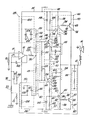
- the circuit provides a transducer output 12 which provides a signal to the transducer or audio speaker 14 which is grounded, or common with respect to the bipolar power supply.
- a power supply or connection is included and comprises a positive voltage supply rail 24 and a negative voltage supply rail 26.
- the positive supply rail 24 is at plus 45 volts and the negative supply rail 26 is provided a minus 45 volts with respect to circuit ground.
- a P channel metal oxide semiconductor-field-effect transistor 32 referred to as a MOS-FET, is in common source connection between the power source 24 and the transducer output 12. More specifically, the P channel MOS-FET 32 has a source 34 connected to the positive voltage rail 24, a drain 36 connected to the transducer output 12 and a gate 38. In a similar fashion, an N channel MOS-FET 40 is in common source connection between the power source 26 and the transducer output 12. The N channel MOS-FET 40 has a source 42 connected to the negative voltage rail 26, a drain 44 connected to the transducer output 12 and a gate 46.
- a positive voltage level-shifting and driver stage 48 is responsive to the output of the operational amplifier 16 for establishing a voltage differential between the gate 38 of the P channel MOS-FET 32 and the positive voltage rail 24 to drive the P channel MOS-FET 32 into conduction.
- a negative voltage level-shifting and driver stage 50 is responsive to the output of the operational amplifier 16 for establishing a voltage differential between the gate 46.pf the N channel MOS-FET 40 and the negative voltage rail 26 to drive the N channel MOS-FET 40 into conduction.
- a system negative feedback circuit interconnecting the transducer output 12 and the operational amplifier 16 on the negative input 17 side for returning a portion of the transducer output voltage to the operational amplifier 16 to cause the transducer output signal to track the signal at the audio input to the operational amplifier 16.
- the positive voltage regulator 28 is of the conventional type including a resistor 100 between the positive supply rail 24 and the zener diode 102 and a capacitor 104 in parallel with the zener diode 102 to ground.
- the negative voltage regulator 30 includes a resistor 106 in series with a zener diode 108 and its parallel capacitor 110 which ares in turn, grounded.
- the negative driver stage 50 includes a driver PNP transistor 134 having its base 136 d.c. coupled by the line 62 to the quiescent current regulating stage 64 to the negative voltage divider 60 at a position between the resistors 116 and 118 thereof.
- the collector 138 of the transistor I34 is connected through the resistor 140 to the gate 46 of the MOS-FET 40 and through the resistor 142 to the negative voltage rail 26.
- the emitter 144 of the transistor 134 is connected through the resistor 146 to the ground 52.
- each driver stage 48 and 50 includes a first resistor 128 and 142 between the gate 38 and 46 of the associated MOS-FET 32 and 40 and the associated power supply rail 24 and 26.
- Each driver stage also includes a second resistor 126 and 142 between the gate 38 and 46 of the associated MOS-FET 32 and 40 and the associated collector 124 and 138 of the associated transistor 120 and 134.
- the second resistors 132 and 146 are commonly connected to the ground 52.
- the resistor 132 is disposed between the connection of the negative feedback circuit 94 to the emitter 130 of the NPN transistor 120 and the ground 52.
- the resistor 146 is disposed between the connection of the negative feedback circuit 96 and the emitter 144 of the PNP transistor 134 and ground 52.
- a capacitor 168 is in a negative feedback loop from the output of the operational amplifier 16 to the negative input 17 side to the operational amplifier 16.
- the capacitor 168 shapes the high frequency response of the amplifier and affords high frequency stability to the amplifier 1 6.
- the resistance 18 between ground and the plus input 15 side of the amplifier 16 along with the resistors in the negative input 17 to the minus side of the operational amplifier 16 establish the voltage reference to ground and the gain of the overall amplifier circuit.
- the voltage regulators 28 and 30 typically provide plus and minus 15 volts to the operational amplifier 16.
- the resistance -170 between the output of . the operational amplifier 16 and the voltage dividers 54 and 60 provides a limitation on the maximum drive current from the operational amplifier 16.
- the circuit 92 would include a 0.1 microfarad capacitor and a 10 ohm resistor.
- the transducer 14 would be an 8 ohm load in series with a 1 microhenry inductor.
- the operational amplifier 16 may be of the type TL081 or LM318 connected in the inverting mode and powered from the zener stabilized bipolar voltage supplies 28 and 30 which include the zener diodes 102 and 108 which provide a plus or minus 15 volts supplied to the operational amplifier 16.
- the output voltage swing of the operational amplifier 16 is normally limited to plus or minus 10 volts peak to peak and is, therefore, amplified by a complementary pair of level-shifting transistors 120 and 134 which may be a 92PU05-npn and a 92PU55-pnp. Each of the transistors 120 and 134 operate with a voltage gain of approximately 4.
- each transistor 120 and 134 nominally 110 micro amps, which is sufficient to bias the base of each transistor 120 and 134 into conduction.
- the high gate input resistance of the MOS-FET transistors 32 and 40 permits the use of high value collector and emitter resistors in the level shifting amplifiers to reduce the running and quiescent currents.
- Each MOF-FET transistor 32 and 40 respectively, a P channel Hitachi 2SJ48 and an N channel Hitachi 1SJ133, is configured to handle approximately 100 milliamps of source-drain current quiescently and up to 1.4 amps of current under full drive at which point the 1 ohm source resistors 78 and 88 exhibit a 1.4 voltage drop.
- the transistors 68 and 82 begin to conduct only when the 1.4 volt base-emitter voltage is reached.
- the transistors 68 and 82 exhibit a very high gain.
- the maximum gain of the output stage is limited by the 22K feedback resistors 156 and 160 which yield a maximum gain of approximately 19 (e.g., resistor 132 plus resistor 156 divided by resistor 132 which is 1.2K plus 22K divided by 1.2K, which equals 19.3).
- the two separate negative feedback circuits 94 and 96 allow a much higher than normal driver stage gain while maintaining high waveform fidelity in the driver stages.
Landscapes
- Engineering & Computer Science (AREA)
- Power Engineering (AREA)
- Amplifiers (AREA)
Applications Claiming Priority (2)
| Application Number | Priority Date | Filing Date | Title |
|---|---|---|---|
| US06/422,260 US4483016A (en) | 1982-09-23 | 1982-09-23 | Audio amplifier |
| US422260 | 1999-10-21 |
Publications (2)
| Publication Number | Publication Date |
|---|---|
| EP0104852A2 true EP0104852A2 (de) | 1984-04-04 |
| EP0104852A3 EP0104852A3 (de) | 1986-07-30 |
Family
ID=23674081
Family Applications (1)
| Application Number | Title | Priority Date | Filing Date |
|---|---|---|---|
| EP83305472A Ceased EP0104852A3 (de) | 1982-09-23 | 1983-09-19 | Tonfrequenzverstärker |
Country Status (4)
| Country | Link |
|---|---|
| US (1) | US4483016A (de) |
| EP (1) | EP0104852A3 (de) |
| JP (1) | JPS59131207A (de) |
| CA (1) | CA1194941A (de) |
Cited By (3)
| Publication number | Priority date | Publication date | Assignee | Title |
|---|---|---|---|---|
| EP0534804A1 (de) * | 1991-09-27 | 1993-03-31 | Exar Corporation | Klasse-D Ausgangsverstärker in BICMOS für Hörhilfegerät |
| EP2963814A1 (de) * | 2014-07-03 | 2016-01-06 | Bang & Olufsen A/S | Klasse-AB-Verstärker mit Vorspannungssteuerung |
| US12375050B2 (en) | 2021-10-12 | 2025-07-29 | Solid State Logic Uk Limited | Amplifying a bipolar input signal |
Families Citing this family (11)
| Publication number | Priority date | Publication date | Assignee | Title |
|---|---|---|---|---|
| US4728903A (en) * | 1986-05-02 | 1988-03-01 | Reiffin Martin G | Class A high-fidelity amplifier |
| US4743860A (en) * | 1987-03-10 | 1988-05-10 | Seeburg Phonograph Corporation | Audio power amplifier |
| US4973916A (en) * | 1987-12-11 | 1990-11-27 | Mcbaik Electronics, Ltd. | Operational amplifier driven power amplifier |
| US4991221A (en) * | 1989-04-13 | 1991-02-05 | Rush James M | Active speaker system and components therefor |
| US4954787A (en) * | 1989-05-18 | 1990-09-04 | Brisson Bruce A | Audio signal transmission system with noise suppression network |
| AT393576B (de) * | 1989-09-28 | 1991-11-11 | Philips Nv | Schaltungsanordnung zur elektronischen pegelsteuerung eines tonsignals |
| US5302917A (en) * | 1993-02-12 | 1994-04-12 | Concorso James A | Linear amplifier circuit for audio equipment |
| US5814953A (en) * | 1995-12-18 | 1998-09-29 | Thomson Consumer Electronics, Inc. | Power amplifier predriver stage |
| US6476678B1 (en) * | 2000-08-04 | 2002-11-05 | Maxim Integrated Products, Inc. | High performance amplifier circuits using separate power supplies |
| US7786799B2 (en) * | 2008-03-21 | 2010-08-31 | Cirrus Logic, Inc. | Trimming technique for high voltage amplifiers using floating low voltage structures |
| US9973180B2 (en) | 2015-12-30 | 2018-05-15 | Industrial Technology Research Institute | Output stage circuit |
Family Cites Families (13)
| Publication number | Priority date | Publication date | Assignee | Title |
|---|---|---|---|---|
| US3601712A (en) * | 1968-12-17 | 1971-08-24 | Bell & Howell Co | Source follower |
| US3924070A (en) * | 1970-03-16 | 1975-12-02 | Webster Electric Co Inc | Voice gated amplifier |
| JPS5838965B2 (ja) * | 1974-10-31 | 1983-08-26 | ソニー株式会社 | ゾウフクカイロ |
| JPS4966057A (de) * | 1972-10-27 | 1974-06-26 | ||
| US3872390A (en) * | 1973-12-26 | 1975-03-18 | Motorola Inc | CMOS operational amplifier with internal emitter follower |
| GB1508228A (en) * | 1974-11-12 | 1978-04-19 | Sony Corp | Transistor circuits |
| JPS5855685B2 (ja) * | 1975-09-03 | 1983-12-10 | 株式会社日立製作所 | ゾウフクカイロ |
| JPS52123848A (en) * | 1976-04-12 | 1977-10-18 | Seiko Epson Corp | Amplifier |
| JPS5437450A (en) * | 1977-08-29 | 1979-03-19 | Hitachi Ltd | Source-follower type mos amplifier circuit |
| US4194165A (en) * | 1978-06-28 | 1980-03-18 | Skulski Peter J | Miniature guitar amplifier |
| JPS5514775A (en) * | 1978-07-18 | 1980-02-01 | Seiko Epson Corp | Amplifier circuit |
| CH631047B (fr) * | 1979-07-13 | Ebauches Electroniques Sa | Amplificateur pour signaux alternatifs. | |
| US4390851A (en) * | 1980-11-25 | 1983-06-28 | Rockwell International Corporation | Monolithic microwave amplifier having active impedance matching |
-
1982
- 1982-09-23 US US06/422,260 patent/US4483016A/en not_active Expired - Fee Related
-
1983
- 1983-09-19 EP EP83305472A patent/EP0104852A3/de not_active Ceased
- 1983-09-22 CA CA000437333A patent/CA1194941A/en not_active Expired
- 1983-09-24 JP JP58176875A patent/JPS59131207A/ja active Pending
Cited By (3)
| Publication number | Priority date | Publication date | Assignee | Title |
|---|---|---|---|---|
| EP0534804A1 (de) * | 1991-09-27 | 1993-03-31 | Exar Corporation | Klasse-D Ausgangsverstärker in BICMOS für Hörhilfegerät |
| EP2963814A1 (de) * | 2014-07-03 | 2016-01-06 | Bang & Olufsen A/S | Klasse-AB-Verstärker mit Vorspannungssteuerung |
| US12375050B2 (en) | 2021-10-12 | 2025-07-29 | Solid State Logic Uk Limited | Amplifying a bipolar input signal |
Also Published As
| Publication number | Publication date |
|---|---|
| EP0104852A3 (de) | 1986-07-30 |
| US4483016A (en) | 1984-11-13 |
| CA1194941A (en) | 1985-10-08 |
| JPS59131207A (ja) | 1984-07-28 |
Similar Documents
| Publication | Publication Date | Title |
|---|---|---|
| EP0715238B1 (de) | Schaltung und Verfahren zur Spannungsregelung | |
| US6791418B2 (en) | Capacitor coupled dynamic bias boosting circuit for a power amplifier | |
| EP0104852A2 (de) | Tonfrequenzverstärker | |
| EP0888670B1 (de) | Linearer hochfrequenzverstärker mit hoher eingangsimpedanz und hohem leistungswirkungsgrad | |
| US6150853A (en) | Integrated unit gain output stage | |
| US5874858A (en) | Amplifier system having a constant current regulating unit | |
| EP0031677A1 (de) | Gegentakt AB-Feldeffekttransistorverstärker | |
| US5166636A (en) | Dynamic biasing for class a amplifier | |
| US4801893A (en) | Forward transimpedance amplifier | |
| KR100712430B1 (ko) | 전계 효과 트랜지스터의 바이어스 회로 | |
| US10855239B2 (en) | Amplifier class AB output stage | |
| US6292057B1 (en) | Output stage of an operational amplifier and method having a latchup-free sourcing current booster for driving low impedance loads | |
| EP0391055A2 (de) | Ausgangsstufe für einen Operationsverstärker | |
| JPS60257610A (ja) | 能動負荷回路 | |
| EP0715405B1 (de) | Verstärkerschaltung und Verfahren | |
| US5828269A (en) | High-frequency amplifier with high input impedance and high power efficiency | |
| JP3273813B2 (ja) | 増幅器 | |
| JPH04307804A (ja) | 単位利得最終段 | |
| US6424220B2 (en) | Single-ended push-pull amplifier circuit | |
| US5684432A (en) | Amplifier output stage having enhanced drive capability | |
| US4345215A (en) | Audio frequency power amplifier circuit | |
| US4560948A (en) | Circuit for increasing voltage gain | |
| US6614306B1 (en) | Bias circuit for class AB high frequency amplifiers | |
| EP0913930A2 (de) | Symmetrische transformatorlose Verstärkerschaltung | |
| US6650183B2 (en) | Amplifier apparatus for an output stage of a laser driver circuit |
Legal Events
| Date | Code | Title | Description |
|---|---|---|---|
| PUAI | Public reference made under article 153(3) epc to a published international application that has entered the european phase |
Free format text: ORIGINAL CODE: 0009012 |
|
| AK | Designated contracting states |
Designated state(s): AT BE CH DE FR GB IT LI LU NL SE |
|
| PUAL | Search report despatched |
Free format text: ORIGINAL CODE: 0009013 |
|
| AK | Designated contracting states |
Kind code of ref document: A3 Designated state(s): AT BE CH DE FR GB IT LI LU NL SE |
|
| 17P | Request for examination filed |
Effective date: 19861029 |
|
| 17Q | First examination report despatched |
Effective date: 19870629 |
|
| STAA | Information on the status of an ep patent application or granted ep patent |
Free format text: STATUS: THE APPLICATION HAS BEEN REFUSED |
|
| 18R | Application refused |
Effective date: 19881118 |