EP0104565B1 - Bestücken gedruckter Leiterplatten mit elektrischen Bauelementen - Google Patents
Bestücken gedruckter Leiterplatten mit elektrischen Bauelementen Download PDFInfo
- Publication number
- EP0104565B1 EP0104565B1 EP83109223A EP83109223A EP0104565B1 EP 0104565 B1 EP0104565 B1 EP 0104565B1 EP 83109223 A EP83109223 A EP 83109223A EP 83109223 A EP83109223 A EP 83109223A EP 0104565 B1 EP0104565 B1 EP 0104565B1
- Authority
- EP
- European Patent Office
- Prior art keywords
- components
- solder
- leads
- circuit board
- pcb
- Prior art date
- Legal status (The legal status is an assumption and is not a legal conclusion. Google has not performed a legal analysis and makes no representation as to the accuracy of the status listed.)
- Expired
Links
Images

Classifications
-
- H—ELECTRICITY
- H05—ELECTRIC TECHNIQUES NOT OTHERWISE PROVIDED FOR
- H05K—PRINTED CIRCUITS; CASINGS OR CONSTRUCTIONAL DETAILS OF ELECTRIC APPARATUS; MANUFACTURE OF ASSEMBLAGES OF ELECTRICAL COMPONENTS
- H05K3/00—Apparatus or processes for manufacturing printed circuits
- H05K3/30—Assembling printed circuits with electric components, e.g. with resistor
- H05K3/32—Assembling printed circuits with electric components, e.g. with resistor electrically connecting electric components or wires to printed circuits
- H05K3/34—Assembling printed circuits with electric components, e.g. with resistor electrically connecting electric components or wires to printed circuits by soldering
- H05K3/341—Surface mounted components
- H05K3/3415—Surface mounted components on both sides of the substrate or combined with lead-in-hole components
-
- H—ELECTRICITY
- H05—ELECTRIC TECHNIQUES NOT OTHERWISE PROVIDED FOR
- H05K—PRINTED CIRCUITS; CASINGS OR CONSTRUCTIONAL DETAILS OF ELECTRIC APPARATUS; MANUFACTURE OF ASSEMBLAGES OF ELECTRICAL COMPONENTS
- H05K3/00—Apparatus or processes for manufacturing printed circuits
- H05K3/30—Assembling printed circuits with electric components, e.g. with resistor
- H05K3/32—Assembling printed circuits with electric components, e.g. with resistor electrically connecting electric components or wires to printed circuits
- H05K3/34—Assembling printed circuits with electric components, e.g. with resistor electrically connecting electric components or wires to printed circuits by soldering
- H05K3/3447—Lead-in-hole components
-
- H—ELECTRICITY
- H05—ELECTRIC TECHNIQUES NOT OTHERWISE PROVIDED FOR
- H05K—PRINTED CIRCUITS; CASINGS OR CONSTRUCTIONAL DETAILS OF ELECTRIC APPARATUS; MANUFACTURE OF ASSEMBLAGES OF ELECTRICAL COMPONENTS
- H05K2203/00—Indexing scheme relating to apparatus or processes for manufacturing printed circuits covered by H05K3/00
- H05K2203/01—Tools for processing; Objects used during processing
- H05K2203/0104—Tools for processing; Objects used during processing for patterning or coating
- H05K2203/0126—Dispenser, e.g. for solder paste, for supplying conductive paste for screen printing or for filling holes
-
- H—ELECTRICITY
- H05—ELECTRIC TECHNIQUES NOT OTHERWISE PROVIDED FOR
- H05K—PRINTED CIRCUITS; CASINGS OR CONSTRUCTIONAL DETAILS OF ELECTRIC APPARATUS; MANUFACTURE OF ASSEMBLAGES OF ELECTRICAL COMPONENTS
- H05K2203/00—Indexing scheme relating to apparatus or processes for manufacturing printed circuits covered by H05K3/00
- H05K2203/14—Related to the order of processing steps
- H05K2203/1446—Treatment after insertion of lead into hole, e.g. bending, cutting, caulking or curing of adhesive but excluding soldering
-
- H—ELECTRICITY
- H05—ELECTRIC TECHNIQUES NOT OTHERWISE PROVIDED FOR
- H05K—PRINTED CIRCUITS; CASINGS OR CONSTRUCTIONAL DETAILS OF ELECTRIC APPARATUS; MANUFACTURE OF ASSEMBLAGES OF ELECTRICAL COMPONENTS
- H05K2203/00—Indexing scheme relating to apparatus or processes for manufacturing printed circuits covered by H05K3/00
- H05K2203/14—Related to the order of processing steps
- H05K2203/1476—Same or similar kind of process performed in phases, e.g. coarse patterning followed by fine patterning
-
- H—ELECTRICITY
- H05—ELECTRIC TECHNIQUES NOT OTHERWISE PROVIDED FOR
- H05K—PRINTED CIRCUITS; CASINGS OR CONSTRUCTIONAL DETAILS OF ELECTRIC APPARATUS; MANUFACTURE OF ASSEMBLAGES OF ELECTRICAL COMPONENTS
- H05K2203/00—Indexing scheme relating to apparatus or processes for manufacturing printed circuits covered by H05K3/00
- H05K2203/15—Position of the PCB during processing
- H05K2203/1572—Processing both sides of a PCB by the same process; Providing a similar arrangement of components on both sides; Making interlayer connections from two sides
-
- H—ELECTRICITY
- H05—ELECTRIC TECHNIQUES NOT OTHERWISE PROVIDED FOR
- H05K—PRINTED CIRCUITS; CASINGS OR CONSTRUCTIONAL DETAILS OF ELECTRIC APPARATUS; MANUFACTURE OF ASSEMBLAGES OF ELECTRICAL COMPONENTS
- H05K3/00—Apparatus or processes for manufacturing printed circuits
- H05K3/30—Assembling printed circuits with electric components, e.g. with resistor
- H05K3/32—Assembling printed circuits with electric components, e.g. with resistor electrically connecting electric components or wires to printed circuits
- H05K3/34—Assembling printed circuits with electric components, e.g. with resistor electrically connecting electric components or wires to printed circuits by soldering
- H05K3/3457—Solder materials or compositions; Methods of application thereof
- H05K3/3485—Applying solder paste, slurry or powder
-
- Y—GENERAL TAGGING OF NEW TECHNOLOGICAL DEVELOPMENTS; GENERAL TAGGING OF CROSS-SECTIONAL TECHNOLOGIES SPANNING OVER SEVERAL SECTIONS OF THE IPC; TECHNICAL SUBJECTS COVERED BY FORMER USPC CROSS-REFERENCE ART COLLECTIONS [XRACs] AND DIGESTS
- Y02—TECHNOLOGIES OR APPLICATIONS FOR MITIGATION OR ADAPTATION AGAINST CLIMATE CHANGE
- Y02P—CLIMATE CHANGE MITIGATION TECHNOLOGIES IN THE PRODUCTION OR PROCESSING OF GOODS
- Y02P70/00—Climate change mitigation technologies in the production process for final industrial or consumer products
- Y02P70/50—Manufacturing or production processes characterised by the final manufactured product
Definitions
- This invention relates to the mounting of electronic components on printed circuit boards, and is particularly concerned with the mounting of leaded components on one side and surface mounted components on the other side of printed circuit boards.
- a printed circuit board comprises a flat sheet-like support member, for example of glass fiber reinforced resin, with electrical circuit patterns on one or both surfaces.
- the components mounted on the PCB may be leaded components or surface mounted components.
- Leaded components have leads extending down from the component, the leads being inserted into holes through the PCB. The ends of the leads extend through to the surface of the PCB remote from the component and are soldered to the circuit pattern on that surface.
- Surface mounted components have contact areas on the components which are connected by solder to solder pads forming part of the circuit pattern on the PCB. Surface mounting components are often first attached to the PCB by adhesive, prior to soldering.
- Surface mounted components can be mounted readily on their own. Solder paste can be applied through a mask, on to contact pads, the components positioned, and then the solder melted, by reflow soldering. Alternatively, surface mounted components are positioned on the PCB with a bead of adhesive between component and board. After curing of the adhesive, the components are soldered to the circuit pattern by wave soldering.
- Leaded components are readily wave soldered after insertion.
- the leaded components are on the upper surface of the PCB and the ends of the leads project through holes in the PCB and in the circuit pattern on the lower surface of the PCB.
- wave soldering is easy and convenient and is effective.
- wave soldering can be carried out, as stated above, but certain problems arise in that the wave of solder has a curved surface and as the board travels over the wave, the wave meets vertical edges of the components. Air can be trapped and poor quality solder joints result.
- the invention provides a very efficient and effective process for the mounting of leaded components and surface mounting components on PCB's, with the different forms of components on either side of the PCB.
- the use of wave soldering is avoided, and high quality solder joints are obtained.
- the present invention comprises inserting leaded components on one side of a PCB, cutting and clinching the ends of the leads on the other side of the PCB, turning the PCB over, applying solder paste at the lead ends and on solder pads at predetermined positions on the circuit pattern on the other side of PCB by individual' ejection of solder paste from individual applicator nozzles, positioning surface mounting components on said other side, and reflow soldering to solder both the leads and the surface mounting components.
- solder pastes having different melting temperatures surface mounting components can then be soldered on to the one side on which are mounted the leaded components. It is further possible to repeat the above process, for leaded components inserted from the other side and surface mounting components mounted on the one side, starting with the PCB in the reverse or upside down position.
- Figure 1 illustrates the application of wave soldering to surface mounted components.
- a PCB support member is indicated at 10, electrical circuit patterns at 11 and a masking layer 12 which defines solder pads 13 on the circuit patterns.
- a bead of adhesive is indicated at 14.
- a component, indicated in dotted outline at 15, is then positioned on the adhesive, which is cured to attach the component to the PCB.
- the PCB is then inverted for wave soldering. This is illustrated in Figure 1 (b).
- the solder wave is indicated at 16 and the PCB, with attached components, is moved over the solder wave, as indicated by arrow A.
- the solder wave eventually meets a front end or edge of a component, as indicated at 16a.
- solder should extend from the metal plated end of the component into the solder pad and in good contact with the related circuit pattern.
- the same sort of problem can arise at the rear end or edge as the solder wave passes over the rear of the component.
- some of the adhesive may sputter or run on to pads 13.
- the solder joint must be strong enough to withstand stresses arising from thermal mismatch between component and PCB. Often hand touch- up is necessary to provide satisfactory joints.
- soldering flux trapped between the component and the PCB is in the least very difficult to remove and can give rise to corrosion problems at a later date.
- reflow soldering using solder pastes applied by screening or stencil printing is now being used to replace wave soldering of surface mounted components but the screen or stencil must be in contact with the PCB.
- FIGs 2 to 5 illustrate the steps in a process whereby the reflow solder technique can be applied.
- the PCB support member is again indicated at 10 and circuit patterns at 11.
- Leaded components, one of which is indicated at 20 are attached by inserting the leads 21 through holes 22 in the PCB and circuit patterns and the leads cut and clinched or crimped, as indicated at 23. The clinching or crimping prevents the components from falling out when the PCB is inverted.
- Figure 3 shows the PCB inverted and with dots of solder paste applied, at 24 on the ends of the leads 21, and at 25 for use with a surface mounted or leadless component.
- the dots of solder paste are applied by an automated applicator which positions the dots of solder paste accurately and in precision-metered amounts.
- FIG 4 illustrates the step in which a leadless or surface mounting component 26 is positioned on the PCB, the metal plated ends of the component in contact with the solder paste dots 25.
- the PCB and components are then "reflow soldered".
- the PCB, components and solder paste are heated to a temperature whereby the solder paste fuses and connects components to circuit patterns.
- This condition is seen in Figure 5, the new soldered joints indicated at 27.
- the heating can be by various means, a typical one being "Vapour Phase Reflow Soldering", in which the PCB's and components are passed through a vapour which is at a predetermined temperature. The characteristics of vapour, and solder paste will be described later.
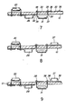
- Figures 6 to 9 illustrate the additional steps which occur when leaded components are also to be mounted on the side of the PCB opposite to the leaded components as illustrated in Figures 2 to 5.
- a further series of circuit patterns 30 are formed on the side opposite to patterns 11.
- Components mounted in the first series of steps, as in Figures 2 to 5, are indicated by the same reference numerals as in Figures 2 to 5.
- a leaded component 31 has been inserted, through holes 32, and the leads 33 cut and crimped, as indicated at 34.
- the PCB is then inverted and dots of solder paste applied, at 35 over the ends of the leads 33, and at positions 36 coincident with the ends of leadless or surface mounting components.
- a leadless component 37 has been positioned on the PCB and in Figure 9 the PCB has been reflow soldered, the solder joints indicated at 38.
- the first reflow soldering is carried out with a solder composed of 63% lead and 34% tin, which is an eutectic alloy and has a melting temperature of 183°C.
- the solder used is composed of 43% lead 43% tin and 14% bismuth, and again is an eutectic alloy.
- the melting point of this solder is between 173 and 174°C.
- the reflow soldering step can be carried out by various forms of heating.
- a liquid supplied by The 3M Company with the designation FC70 has a vapour the maximum temperature of which is 215°C. This temperature is used in the reflow soldering of the 63/67 solder. The temperature is the maximum which the vapour can attain.
- FC43 a liquid supplied by The 3M Company with the designation FC43 is used. The maximum temperature the vapour of this liquid can attain is 174°C. As the solders are eutectic alloys, the melting points are well and tightly defined. Thus the vapour temperature of 174°C will readily reflowthe 43/43/ 14 solder used for the second series of components, but will not affect the 63/37 solder joints for the first series of components.
- Infra-red heating Another form of heating is infra-red heating. This form of heating can be closely controlled and different temperatures can be obtained for the different melting point solders. Infra-red heating also enables temperatures to be attained which cannot be attained with a vapour. Some solders may require higher temperatures than those obtainable with a vapour and infra-red heating is one way of meeting such requirements. Other forms of heating can also be used.
- the invention avoids the use of wave soldering with its accompanying problems.
- the entire process can be automated, including insertion, cutting and crimping of leaded components, application of solder paste, positioning of leadless or surface mounting components and reflow soldering. High yields are obtained.
- the application of the solder paste can be accurately controlled in quantity and precisely positioned, as by optical scanning. Depending upon the number of boards to be processed and the number and positioning of solder joints multiple head applicators can be used.
- the leaded components may comprise electronic components, such as large scale integrated circuits on chips and other electronic devices, and also electrical components_such as connectors, transformers and other devices.
- the leadless components, or surface mounting components may comprise resistors, capacitors and also integrated circuits with leadless encapsulation.
Landscapes
- Engineering & Computer Science (AREA)
- Manufacturing & Machinery (AREA)
- Microelectronics & Electronic Packaging (AREA)
- Electric Connection Of Electric Components To Printed Circuits (AREA)
Claims (5)
Applications Claiming Priority (2)
| Application Number | Priority Date | Filing Date | Title |
|---|---|---|---|
| CA000412029A CA1177972A (en) | 1982-09-23 | 1982-09-23 | Mounting of electronic components on printed circuit boards |
| CA412029 | 1982-09-23 |
Publications (3)
| Publication Number | Publication Date |
|---|---|
| EP0104565A2 EP0104565A2 (de) | 1984-04-04 |
| EP0104565A3 EP0104565A3 (en) | 1984-10-03 |
| EP0104565B1 true EP0104565B1 (de) | 1986-09-17 |
Family
ID=4123648
Family Applications (1)
| Application Number | Title | Priority Date | Filing Date |
|---|---|---|---|
| EP83109223A Expired EP0104565B1 (de) | 1982-09-23 | 1983-09-17 | Bestücken gedruckter Leiterplatten mit elektrischen Bauelementen |
Country Status (4)
| Country | Link |
|---|---|
| EP (1) | EP0104565B1 (de) |
| JP (1) | JPS5974696A (de) |
| CA (1) | CA1177972A (de) |
| DE (1) | DE3366308D1 (de) |
Cited By (4)
| Publication number | Priority date | Publication date | Assignee | Title |
|---|---|---|---|---|
| FR2556550A1 (fr) * | 1983-12-09 | 1985-06-14 | Lignes Telegraph Telephon | Procede de brasage de composants electroniques sur un circuit imprime et circuit hybride obtenu par ce procede |
| EP0263943A1 (de) * | 1986-09-15 | 1988-04-20 | International Business Machines Corporation | Verfahren zum Auflöten von Bauelementen mit Verbindungsdrähten und solchen, die auf eine Oberfläche montiert werden, auf eine Leiterplatte |
| EP0332567A1 (de) * | 1988-03-11 | 1989-09-13 | Lothar Himmelreich | Infrarot-Lötofen zum Aufschmelzlöten von elektronischen Bauelementen auf Leiterplatten |
| EP0415527A2 (de) * | 1989-08-28 | 1991-03-06 | Hewlett-Packard Company | Befestigungsvorrichtung für eine gedruckte Schaltungsplatte |
Families Citing this family (6)
| Publication number | Priority date | Publication date | Assignee | Title |
|---|---|---|---|---|
| JPS6285493A (ja) * | 1985-10-09 | 1987-04-18 | ソニー株式会社 | 電子部品の半田付け方法 |
| DE3720925A1 (de) * | 1987-06-25 | 1989-01-05 | Wabco Westinghouse Fahrzeug | Leiterplatte |
| DE19511226A1 (de) * | 1995-03-27 | 1996-10-02 | Bosch Gmbh Robert | SMD-Verbindung für elektronische Steuergeräte in Kraftfahrzeugen |
| DE10134379A1 (de) | 2001-07-14 | 2003-01-30 | Hella Kg Hueck & Co | Verfahren zur Herstellung einer elektrischen Verbindung zwischen einem Steckerelement und einer Leiterplatte |
| WO2009087113A1 (fr) * | 2008-01-12 | 2009-07-16 | Johnson Controls Technology Company | Procede de montage d'un composant electrique comprenant au moins deux broches de raccordement electrique sur un element de support comprenant au moins deux evidements et raccordement electrique entre un composant electrique et un element de support |
| CN112867388B (zh) * | 2021-01-15 | 2022-05-13 | 深圳市格林赛德科技有限公司 | 一种集成电路加工贴片装置 |
Family Cites Families (3)
| Publication number | Priority date | Publication date | Assignee | Title |
|---|---|---|---|---|
| JPS5376372A (en) * | 1976-12-17 | 1978-07-06 | Matsushita Electric Ind Co Ltd | Device for attaching chip circuit parts |
| JPS5415174A (en) * | 1977-07-06 | 1979-02-03 | Hitachi Ltd | Method of soldering hybrid integrated circuit |
| JPS5754389A (ja) * | 1980-09-19 | 1982-03-31 | Hitachi Ltd | Kairokibannohandazukehoho |
-
1982
- 1982-09-23 CA CA000412029A patent/CA1177972A/en not_active Expired
-
1983
- 1983-09-17 EP EP83109223A patent/EP0104565B1/de not_active Expired
- 1983-09-17 DE DE8383109223T patent/DE3366308D1/de not_active Expired
- 1983-09-20 JP JP58172319A patent/JPS5974696A/ja active Pending
Cited By (5)
| Publication number | Priority date | Publication date | Assignee | Title |
|---|---|---|---|---|
| FR2556550A1 (fr) * | 1983-12-09 | 1985-06-14 | Lignes Telegraph Telephon | Procede de brasage de composants electroniques sur un circuit imprime et circuit hybride obtenu par ce procede |
| EP0263943A1 (de) * | 1986-09-15 | 1988-04-20 | International Business Machines Corporation | Verfahren zum Auflöten von Bauelementen mit Verbindungsdrähten und solchen, die auf eine Oberfläche montiert werden, auf eine Leiterplatte |
| EP0332567A1 (de) * | 1988-03-11 | 1989-09-13 | Lothar Himmelreich | Infrarot-Lötofen zum Aufschmelzlöten von elektronischen Bauelementen auf Leiterplatten |
| EP0415527A2 (de) * | 1989-08-28 | 1991-03-06 | Hewlett-Packard Company | Befestigungsvorrichtung für eine gedruckte Schaltungsplatte |
| EP0415527A3 (en) * | 1989-08-28 | 1992-04-08 | Hewlett-Packard Company | Printed circuit board fixture |
Also Published As
| Publication number | Publication date |
|---|---|
| JPS5974696A (ja) | 1984-04-27 |
| EP0104565A2 (de) | 1984-04-04 |
| CA1177972A (en) | 1984-11-13 |
| EP0104565A3 (en) | 1984-10-03 |
| DE3366308D1 (en) | 1986-10-23 |
Similar Documents
| Publication | Publication Date | Title |
|---|---|---|
| US4515304A (en) | Mounting of electronic components on printed circuit boards | |
| US5155904A (en) | Reflow and wave soldering techniques for bottom side components | |
| EP0263943B1 (de) | Verfahren zum Auflöten von Bauelementen mit Verbindungsdrähten und solchen, die auf eine Oberfläche montiert werden, auf eine Leiterplatte | |
| US5271548A (en) | Method for applying solder to and mounting components on printed circuit boards | |
| US5172852A (en) | Soldering method | |
| US4934582A (en) | Method and apparatus for removing solder mounted electronic components | |
| CN108337821A (zh) | 一种电路板的焊接方法 | |
| US4928387A (en) | Temporary soldering aid for manufacture of printed wiring assemblies | |
| EP0104565B1 (de) | Bestücken gedruckter Leiterplatten mit elektrischen Bauelementen | |
| EP0947125B1 (de) | Verfahren zum herstellen einer leiterplatteranordnung mit zinn/bleischicht | |
| US6310780B1 (en) | Surface mount assembly for electronic components | |
| US5411199A (en) | Method for attaching a shield | |
| US4463407A (en) | Surface mounted electronic components having pre-applied solder | |
| US5373113A (en) | Solder reflow mounting board | |
| JP2646688B2 (ja) | 電子部品の半田付け方法 | |
| EP0245713A1 (de) | Lötflecken zum Benutzen auf einer gedruckten Leiterplatte | |
| JPH06275944A (ja) | 半田付け方法 | |
| JPH0738246A (ja) | はんだ付け方法及び該方法に用いる成形はんだ | |
| JPH05259631A (ja) | プリント配線板の表面実装方法 | |
| JPH09214115A (ja) | ファインピッチ部品のはんだコート方法 | |
| JPS6088495A (ja) | 配線基板 | |
| JPS6333319B2 (de) | ||
| GB2325092A (en) | Preventing distortion during the manufacture of flexible circuit assemblies | |
| JPS63299855A (ja) | ハンダ付け方法 | |
| JPH0722742A (ja) | プリント配線板の半田付け方法 |
Legal Events
| Date | Code | Title | Description |
|---|---|---|---|
| PUAI | Public reference made under article 153(3) epc to a published international application that has entered the european phase |
Free format text: ORIGINAL CODE: 0009012 |
|
| AK | Designated contracting states |
Designated state(s): DE FR GB |
|
| PUAL | Search report despatched |
Free format text: ORIGINAL CODE: 0009013 |
|
| AK | Designated contracting states |
Designated state(s): DE FR GB |
|
| 17P | Request for examination filed |
Effective date: 19840928 |
|
| GRAA | (expected) grant |
Free format text: ORIGINAL CODE: 0009210 |
|
| AK | Designated contracting states |
Kind code of ref document: B1 Designated state(s): DE FR GB |
|
| REF | Corresponds to: |
Ref document number: 3366308 Country of ref document: DE Date of ref document: 19861023 |
|
| EN | Fr: translation not filed | ||
| PLBE | No opposition filed within time limit |
Free format text: ORIGINAL CODE: 0009261 |
|
| STAA | Information on the status of an ep patent application or granted ep patent |
Free format text: STATUS: NO OPPOSITION FILED WITHIN TIME LIMIT |
|
| 26N | No opposition filed | ||
| PGFP | Annual fee paid to national office [announced via postgrant information from national office to epo] |
Ref country code: FR Payment date: 19900919 Year of fee payment: 8 |
|
| PGFP | Annual fee paid to national office [announced via postgrant information from national office to epo] |
Ref country code: DE Payment date: 19901031 Year of fee payment: 8 |
|
| ET | Fr: translation filed | ||
| REG | Reference to a national code |
Ref country code: FR Ref legal event code: BR |
|
| PG25 | Lapsed in a contracting state [announced via postgrant information from national office to epo] |
Ref country code: FR Effective date: 19920529 |
|
| PG25 | Lapsed in a contracting state [announced via postgrant information from national office to epo] |
Ref country code: DE Effective date: 19920602 |
|
| REG | Reference to a national code |
Ref country code: FR Ref legal event code: ST |
|
| PGFP | Annual fee paid to national office [announced via postgrant information from national office to epo] |
Ref country code: GB Payment date: 19980910 Year of fee payment: 16 |
|
| PG25 | Lapsed in a contracting state [announced via postgrant information from national office to epo] |
Ref country code: GB Free format text: LAPSE BECAUSE OF NON-PAYMENT OF DUE FEES Effective date: 19990917 |
|
| GBPC | Gb: european patent ceased through non-payment of renewal fee |
Effective date: 19990917 |