EP0100677A2 - Halbleiteranordnungen mit Lateraltransistoren - Google Patents
Halbleiteranordnungen mit Lateraltransistoren Download PDFInfo
- Publication number
- EP0100677A2 EP0100677A2 EP83304446A EP83304446A EP0100677A2 EP 0100677 A2 EP0100677 A2 EP 0100677A2 EP 83304446 A EP83304446 A EP 83304446A EP 83304446 A EP83304446 A EP 83304446A EP 0100677 A2 EP0100677 A2 EP 0100677A2
- Authority
- EP
- European Patent Office
- Prior art keywords
- region
- emitter
- collector
- base region
- isolation region
- Prior art date
- Legal status (The legal status is an assumption and is not a legal conclusion. Google has not performed a legal analysis and makes no representation as to the accuracy of the status listed.)
- Granted
Links
Images


Classifications
-
- H—ELECTRICITY
- H10—SEMICONDUCTOR DEVICES; ELECTRIC SOLID-STATE DEVICES NOT OTHERWISE PROVIDED FOR
- H10D—INORGANIC ELECTRIC SEMICONDUCTOR DEVICES
- H10D64/00—Electrodes of devices having potential barriers
- H10D64/111—Field plates
-
- H—ELECTRICITY
- H10—SEMICONDUCTOR DEVICES; ELECTRIC SOLID-STATE DEVICES NOT OTHERWISE PROVIDED FOR
- H10B—ELECTRONIC MEMORY DEVICES
- H10B10/00—Static random access memory [SRAM] devices
- H10B10/10—SRAM devices comprising bipolar components
-
- H—ELECTRICITY
- H10—SEMICONDUCTOR DEVICES; ELECTRIC SOLID-STATE DEVICES NOT OTHERWISE PROVIDED FOR
- H10D—INORGANIC ELECTRIC SEMICONDUCTOR DEVICES
- H10D10/00—Bipolar junction transistors [BJT]
- H10D10/60—Lateral BJTs
-
- H—ELECTRICITY
- H10—SEMICONDUCTOR DEVICES; ELECTRIC SOLID-STATE DEVICES NOT OTHERWISE PROVIDED FOR
- H10D—INORGANIC ELECTRIC SEMICONDUCTOR DEVICES
- H10D62/00—Semiconductor bodies, or regions thereof, of devices having potential barriers
- H10D62/10—Shapes, relative sizes or dispositions of the regions of the semiconductor bodies; Shapes of the semiconductor bodies
- H10D62/17—Semiconductor regions connected to electrodes not carrying current to be rectified, amplified or switched, e.g. channel regions
- H10D62/177—Base regions of bipolar transistors, e.g. BJTs or IGBTs
- H10D62/184—Base regions of bipolar transistors, e.g. BJTs or IGBTs of lateral BJTs
-
- H10W10/00—
-
- H10W10/01—
-
- H10W10/031—
-
- H10W10/30—
Definitions
- the present invention relates to semiconductor devices including lateral-type transistors.
- lateral-type transistors are transistors in which both an emitter and a collector are arranged on the same surface layer of the semiconductor substrate. This type of transistor is used, for example, as a load element in the memory cells of some memory circuits.
- PNP transistor lateral-type PNP transistors
- Such PNP transistors may suffer From so-called channel leakage. Channel leakage is caused by conduction between the emitter and collector of a PNP transistor that arises when negative (-) charges (usually called “contamination”) are injected into an insulation layer formed on the base region. It should be understood that this problem of channel leakage is already well known.
- the above-mentioned positive electrode may easily be formed above the base region when the IC is not densely packaged.
- the smallness of the area that is generally available for mounting the positive electrodes may make it difficult to ensure that these positive electrodes are able to achieve their intended function of preventing channel leakage.
- An embodiment of the present invention can be made to provide a lateral-type PNP transistor having a P-type collector region, a P-type emitter region, and an N-type base region, all of which contact an isolation region, the isolation region projecting partially into just said base region.
- transistors Q 1 and Q 2 each of which is a load element of the memory cell MC.
- the load element was usually a load resistor.
- the trend of late has been to use a load transistor as the load element.
- Each of these load transistors Q1 and Q 2 corresponds to the above.lateral-type PNP transistor, in which the above-mentioned problem of channel leakage occurs.
- Figure 2 is a cross-sectional view of a lateral-type PNP transistor which illustrates the problem of channel leakage inherent therein (Fig. 2 is similar to the view taken along line 2-2 in Fig. 3 mentioned hereinafter).
- the reference numeral 21 represents a semiconductor substrate composed of, for example, an epitaxial layer 22 and an N-type layer 23.
- the reference numeral 24 represents an isolation region for electrically separating adjacent circuit elements from each other.
- an emitter E and a collector C are formed, respectively, as P-type regions 25 and 26 by a diffusion process whereby both emitter E and collector C are arranged on the same surface layer.
- an insulation layer 27 is formed on the surface of the semiconductor substrate 21; it should be recognized that, during the process for forming this insulation layer 27, negative charges are sometimes injected thereinto. If the negative charges thus injected are located above the base region B, since, as previously mentioned, the PNP transistors also behave as P-channel MOS transistors, the path between the emitter E and the collector C becomes conductive, resulting in channel leakage. In order to avoid such channel leakage, an electrode having a positive voltage is usually mounted above the base region B, such as to attract the negative charges to the upper side of insulation layer 27 (see dashed lines). In this case, it is economically preferable to fabricate this positive electrode integral with an emitter wiring 28. This is because, in conventional PNP transistors, the emitter always receives a positive voltage. The emitter wiring 28 is thus distributed such that it covers not only the emitter region E, but also the base region B, as shown in Fig. 2.
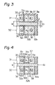
- Figure 3 is a plan view of a conventional lateral--type PNP transistor having a cross-section similar to that of the transistor shown in Fig. 2. It should be noted that Fig. 3 exemplifies an arrangement where two PNP transistors (corresponding to Q 1 and Q 2 of Fig. 1) face each other across an isolation region, sandwiched therebetween, such as to conform with the circuit arrangement of Fig. 1.
- reference numeral 31 represents a first lateral-type PNP transistor that faces a second lateral-type PNP transistor 32 across an isolation region 33 sandwiched therebetween.
- reference characters 31c, 31b and 3le are respectively a collector region, a base region, and an emitter region thereof, while reference symbols C 1 and E 1 , enclosed by square lines, represent a collector contact and an emitter contact, respectively.
- reference characters 32c, 32b and 32e respectively represent a collector region, a base region, and an emitter region, while reference symbols C 2 and E 2 , enclosed by square lines, represent a collector contact and an emitter contact, respectively.
- Reference numerals 35 and 36 represent collector wirings, while reference numerals 37 and 38 represent emitter wirings.
- hatched lines and dotted areas are used, not for the usual purpose of representing regions in cross- section, but to help the viewer distinguish between the different components.
- embodiments of the invention particularly concern portions 37 L and 38 Q , i.e., the above--mentioned positive electrodes for preventing channel leakage that extend from respective emitter wirings 37 and 38 to completely cover respective base regions 31 b and 32 b .
- Self-alignment is generally well known as a means for achieving high IC packing densities.
- the arrangement illustrated in Fig. 2 was also created with the aid of self-alignment.
- the diffusion areas for forming collector regions 31c and 32 c and emitter regions 31 e and 32 e are self-aligned by isolation region 33.
- the pattern densities in the IC can be considerably increased.
- recent demand for higher pattern densities has grown very strong, as a result of which an attempt is often made to set the width W of the isolation region 33 smaller than usual. This inevitably results, however, in bringing emitter wirings 37 and 38 closer to each other, increasing the likelihood of an electric short therebetween.
- An embodiment of the present invention can provide a semiconductor device in which the width W of the isolation region is reduced for higher pattern densities and channel leakage prevented from occurring therein by a very simple means.
- Figure 4 is a plan view showing an embodiment of a semiconductor device according to the present invention.
- members are represented by the same reference numerals or characters as the corresponding members in Fig. 3; these numerals and characters are used to represent like members in the later figures as well.
- the only difference between the embodiments shown in Figs. 3 and 4 lies in an isolation region 41.
- the width w of this isolation layer 41 is narrower than the width W of the isolation region in Fig. 3.
- the smaller width w is intended to allow higher pattern densities.
- the smaller the width of the isolation region the closer the emitter wirings 37 and 38 approach to each other. In the worst case, these emitter wirings may become electrically shorted on account of a variance in wiring size during manufacturing. To avoid such shorting, the width of each emitter wiring must be made as small as possible, such as to reduce the width D of margin of the wirings (see Fig. 3) to essentially zero.
- portions not covered by the extended emitter wirings 37 l and 38 t may be formed above the base regions due to variances in wiring dimensions arising during manufacturing, causing the base regions to be left at least partially uncovered. If such uncovered portions exist, channel leakage will tend to occur.
- the width of isolation region 41 is widened somewhat at the portion facing each of the base regions by providing projections 42 and 43 of the isolation region 41, said projections extending from the body of isolation region 41 into respective base regions 31 b and 32 b .
- base regions 31 b and 32 b are manufactured with considerably small widths due to variances in the manufacturing process, they remain completely covered by respective extended emitter wirings 37 l and 38 l , which can prevent channel leakage from occurring.
- Figure 5 is a plan view of a semiconductor device identical with that of Fig. 4, except that it is manufactured with wiring of a different size.
- wirings 31 , 32 e , 37 l , and 38 l are manufactured at the minimum limit in a predetermined range in allowable design size, this limit corresponding to the worst possible case of wiring size variance during the manufacturing process.
- the side of emitter wiring 31 e provided with electrode 37 1 is located far from one side of the body of isolation region 41.
- this also applies to the sides of wirings 32 e and 38 l with respect to the other side of region 41.
- the base region 31 b can still be completely covered by electrode 37 l because one side of base region 31 b is located apart from one side of the body of isolation region 41 facing thereto.
- Figure 6 is a plan view of one example of an application based on the embodiment of Fig. 4.
- three or more identical PNP transistors are fabricated according to the present invention.
- the third PNP transistor is represented as a whole by reference numeral 62.
- Reference numerals 53 and 63 represent the projections constituting a feature of the present invention.
- Members C 3 ' B 3 ' and E3 are identical to members C 1' C 2 ' B 1 ' B 2 ' and E 1 , E2.
- the members represented by reference characters 62 c , 68 l , 62 , and 66 are identical respectively to members 32 c 38 l , 32 e , and 36 shown in Figs. 4 and 5.
- Figure 7 is a plan view of another example of an application based on the embodiment of Fig. 4.
- the PNP transistor 31 does not face another PNP transistor, but rather conductor lead 71, with isolation region 41 sandwiched therebetween.
- the width D (Fig. 3) of margin in the wiring should be reduced to substantially zero. This results in the formation of an uncovered portion above the base region 31 b in the absence of projection 42.
- embodiments of the present invention can provide a simple means for attaining high IC packaging densities while protecting against channel leakage.
Landscapes
- Bipolar Transistors (AREA)
- Bipolar Integrated Circuits (AREA)
- Static Random-Access Memory (AREA)
- Element Separation (AREA)
- Semiconductor Memories (AREA)
Applications Claiming Priority (2)
| Application Number | Priority Date | Filing Date | Title |
|---|---|---|---|
| JP133780/82 | 1982-08-02 | ||
| JP57133780A JPS5925241A (ja) | 1982-08-02 | 1982-08-02 | Pnpトランジスタ |
Publications (3)
| Publication Number | Publication Date |
|---|---|
| EP0100677A2 true EP0100677A2 (de) | 1984-02-15 |
| EP0100677A3 EP0100677A3 (en) | 1986-10-29 |
| EP0100677B1 EP0100677B1 (de) | 1989-03-22 |
Family
ID=15112810
Family Applications (1)
| Application Number | Title | Priority Date | Filing Date |
|---|---|---|---|
| EP83304446A Expired EP0100677B1 (de) | 1982-08-02 | 1983-08-01 | Halbleiteranordnungen mit Lateraltransistoren |
Country Status (4)
| Country | Link |
|---|---|
| EP (1) | EP0100677B1 (de) |
| JP (1) | JPS5925241A (de) |
| DE (1) | DE3379492D1 (de) |
| IE (1) | IE54677B1 (de) |
Cited By (1)
| Publication number | Priority date | Publication date | Assignee | Title |
|---|---|---|---|---|
| EP0247386A3 (en) * | 1986-05-30 | 1988-03-16 | Telefunken Electronic Gmbh | Lateral transistor |
Family Cites Families (1)
| Publication number | Priority date | Publication date | Assignee | Title |
|---|---|---|---|---|
| JPS567463A (en) * | 1979-06-29 | 1981-01-26 | Hitachi Ltd | Semiconductor device and its manufacture |
-
1982
- 1982-08-02 JP JP57133780A patent/JPS5925241A/ja active Granted
-
1983
- 1983-08-01 DE DE8383304446T patent/DE3379492D1/de not_active Expired
- 1983-08-01 EP EP83304446A patent/EP0100677B1/de not_active Expired
- 1983-08-02 IE IE1825/83A patent/IE54677B1/en unknown
Cited By (2)
| Publication number | Priority date | Publication date | Assignee | Title |
|---|---|---|---|---|
| EP0247386A3 (en) * | 1986-05-30 | 1988-03-16 | Telefunken Electronic Gmbh | Lateral transistor |
| US4829356A (en) * | 1986-05-30 | 1989-05-09 | Telefunken Electronic Gmbh | Lateral transistor with buried semiconductor zone |
Also Published As
| Publication number | Publication date |
|---|---|
| DE3379492D1 (en) | 1989-04-27 |
| JPS5925241A (ja) | 1984-02-09 |
| EP0100677B1 (de) | 1989-03-22 |
| IE54677B1 (en) | 1990-01-03 |
| IE831825L (en) | 1984-02-02 |
| JPH0420259B2 (de) | 1992-04-02 |
| EP0100677A3 (en) | 1986-10-29 |
Similar Documents
| Publication | Publication Date | Title |
|---|---|---|
| EP0161983B1 (de) | Eingangs-Schutzanordnung für VLSI-Schaltungsanordnungen | |
| US4926243A (en) | High voltage MOS field effect semiconductor device | |
| KR100294412B1 (ko) | 실리콘온인슐레이터(soi)구조를갖는입/출력보호회로 | |
| EP0551712B1 (de) | Halbleiteranordnung mit Feldplatten | |
| US4969020A (en) | Semiconductor device | |
| KR910000229B1 (ko) | 보호장치를 구비하고 있는 반도체집적회로와 그 제조방법 | |
| US4520382A (en) | Semiconductor integrated circuit with inversion preventing electrode | |
| GB2199185A (en) | Semiconductor device with junction breakdown protection | |
| EP0100677B1 (de) | Halbleiteranordnungen mit Lateraltransistoren | |
| EP0198468A2 (de) | Schutzanordnung für eine integrierte Schaltung | |
| US8329548B2 (en) | Field transistors for electrostatic discharge protection and methods for fabricating the same | |
| KR19980070010A (ko) | 향상된 트랜지스터 구조물을 가지며 그 점유 영역을 크게 감소시키는 것이 가능한 반도체 장치 및 그 제조 방법 | |
| US4952998A (en) | Integrated circuit with complementary MOS transistors | |
| EP0149065A2 (de) | Schutz-Blockierschaltung für eine monolitische Schaltung zur Verhinderung von Spitzenströmen | |
| JPS6230704B2 (de) | ||
| KR100238376B1 (ko) | 정전기 방지용 트랜지스터 및 그 제조방법 | |
| US5444283A (en) | Dopant-diffusion buffered buried contact module for integrated circuits | |
| JPH01185974A (ja) | Mis−fet | |
| KR930011129B1 (ko) | Ppl셀로 구성한 sram소자 및 그 제조방법 | |
| KR100290788B1 (ko) | 반도체 소자의 정전기 방지 구조 | |
| KR100249016B1 (ko) | 반도체장치의 이에스디 보호회로 제조방법 | |
| KR200183767Y1 (ko) | 반도체 소자 | |
| JPH07112043B2 (ja) | 半導体集積回路 | |
| JPH0499371A (ja) | 半導体装置 | |
| JPS6223459B2 (de) |
Legal Events
| Date | Code | Title | Description |
|---|---|---|---|
| PUAI | Public reference made under article 153(3) epc to a published international application that has entered the european phase |
Free format text: ORIGINAL CODE: 0009012 |
|
| AK | Designated contracting states |
Designated state(s): DE FR GB |
|
| PUAL | Search report despatched |
Free format text: ORIGINAL CODE: 0009013 |
|
| AK | Designated contracting states |
Kind code of ref document: A3 Designated state(s): DE FR GB |
|
| 17P | Request for examination filed |
Effective date: 19870213 |
|
| 17Q | First examination report despatched |
Effective date: 19880803 |
|
| GRAA | (expected) grant |
Free format text: ORIGINAL CODE: 0009210 |
|
| AK | Designated contracting states |
Kind code of ref document: B1 Designated state(s): DE FR GB |
|
| REF | Corresponds to: |
Ref document number: 3379492 Country of ref document: DE Date of ref document: 19890427 |
|
| ET | Fr: translation filed | ||
| PLBE | No opposition filed within time limit |
Free format text: ORIGINAL CODE: 0009261 |
|
| STAA | Information on the status of an ep patent application or granted ep patent |
Free format text: STATUS: NO OPPOSITION FILED WITHIN TIME LIMIT |
|
| 26N | No opposition filed | ||
| PGFP | Annual fee paid to national office [announced via postgrant information from national office to epo] |
Ref country code: GB Payment date: 19900703 Year of fee payment: 8 |
|
| PGFP | Annual fee paid to national office [announced via postgrant information from national office to epo] |
Ref country code: FR Payment date: 19900830 Year of fee payment: 8 |
|
| PG25 | Lapsed in a contracting state [announced via postgrant information from national office to epo] |
Ref country code: GB Effective date: 19910801 |
|
| GBPC | Gb: european patent ceased through non-payment of renewal fee | ||
| PG25 | Lapsed in a contracting state [announced via postgrant information from national office to epo] |
Ref country code: FR Effective date: 19920430 |
|
| REG | Reference to a national code |
Ref country code: FR Ref legal event code: ST |
|
| PGFP | Annual fee paid to national office [announced via postgrant information from national office to epo] |
Ref country code: DE Payment date: 19921021 Year of fee payment: 10 |
|
| PG25 | Lapsed in a contracting state [announced via postgrant information from national office to epo] |
Ref country code: DE Effective date: 19940503 |