EP0149065A2 - Schutz-Blockierschaltung für eine monolitische Schaltung zur Verhinderung von Spitzenströmen - Google Patents
Schutz-Blockierschaltung für eine monolitische Schaltung zur Verhinderung von Spitzenströmen Download PDFInfo
- Publication number
- EP0149065A2 EP0149065A2 EP84114209A EP84114209A EP0149065A2 EP 0149065 A2 EP0149065 A2 EP 0149065A2 EP 84114209 A EP84114209 A EP 84114209A EP 84114209 A EP84114209 A EP 84114209A EP 0149065 A2 EP0149065 A2 EP 0149065A2
- Authority
- EP
- European Patent Office
- Prior art keywords
- epitaxial
- circuit
- isolated
- substrate
- regions
- Prior art date
- Legal status (The legal status is an assumption and is not a legal conclusion. Google has not performed a legal analysis and makes no representation as to the accuracy of the status listed.)
- Withdrawn
Links
Images

Classifications
-
- H—ELECTRICITY
- H10—SEMICONDUCTOR DEVICES; ELECTRIC SOLID-STATE DEVICES NOT OTHERWISE PROVIDED FOR
- H10D—INORGANIC ELECTRIC SEMICONDUCTOR DEVICES
- H10D89/00—Aspects of integrated devices not covered by groups H10D84/00 - H10D88/00
- H10D89/60—Integrated devices comprising arrangements for electrical or thermal protection, e.g. protection circuits against electrostatic discharge [ESD]
-
- H—ELECTRICITY
- H03—ELECTRONIC CIRCUITRY
- H03K—PULSE TECHNIQUE
- H03K17/00—Electronic switching or gating, i.e. not by contact-making and –breaking
- H03K17/08—Modifications for protecting switching circuit against overcurrent or overvoltage
- H03K17/081—Modifications for protecting switching circuit against overcurrent or overvoltage without feedback from the output circuit to the control circuit
- H03K17/0812—Modifications for protecting switching circuit against overcurrent or overvoltage without feedback from the output circuit to the control circuit by measures taken in the control circuit
- H03K17/08126—Modifications for protecting switching circuit against overcurrent or overvoltage without feedback from the output circuit to the control circuit by measures taken in the control circuit in bipolar transitor switches
-
- H—ELECTRICITY
- H10—SEMICONDUCTOR DEVICES; ELECTRIC SOLID-STATE DEVICES NOT OTHERWISE PROVIDED FOR
- H10D—INORGANIC ELECTRIC SEMICONDUCTOR DEVICES
- H10D84/00—Integrated devices formed in or on semiconductor substrates that comprise only semiconducting layers, e.g. on Si wafers or on GaAs-on-Si wafers
- H10D84/60—Integrated devices formed in or on semiconductor substrates that comprise only semiconducting layers, e.g. on Si wafers or on GaAs-on-Si wafers characterised by the integration of at least one component covered by groups H10D10/00 or H10D18/00, e.g. integration of BJTs
- H10D84/611—Combinations of BJTs and one or more of diodes, resistors or capacitors
- H10D84/613—Combinations of vertical BJTs and one or more of diodes, resistors or capacitors
Definitions
- the present invention relates to protection circuits for use in monolithic integrated circuits. More particularly, the present invention relates to a protection circuit which inhibits turn on of a parasitic silicon controlled rectifier (.SCR) which can be formed in the monolithic circuit containing diffused resistors within "floating" epitaxial tubs.
- a parasitic silicon controlled rectifier .SCR
- IC integrated circuits
- MC1489 Line Receiver that is manufactured by Motorola, Inc. which is schematically illustrated in FIG. 1.
- the MC1489 comprises an input resistor which is coupled between an external pin of the IC to the base of an internal input transistor thereof.
- This resistor is diffused into a separate region of the epitaxial layer of the IC which is isolated from other epitaxial regions or tubs by use of diffusion islands as is well known thereby forming an epitaxial tub with no preohmic contact to the epitaxial tub (hereafter referred to as a "floating" epi. island).
- the substrate of the IC is connected to an additional external pin through one of the isolation regions and is intended to be grounded during normal applications of the IC.
- the operating potential for the IC is connected through an external pin to another one of the isolated epitaxial tubs of the IC.
- IC manufacturers usually evaluate their'IC's after -final package assembly to ensure that the IC's meet electrical specifications. Such testing may include inserting and removing the IC from a "hot socket" which has a test input signal and power supply voltages continually supplied thereto. It has been found that if the substrate of the IC, as described above, is not grounded, as can happen while inserting or removing the 1C from the hot socket, that a failure mode may occur which can damage or even destroy the IC. This failure mode results from a parasitic SCR that is associated with the floating epitaxial tub in which the resistor is formed.
- a protection circuit to inhibit or at least severely limit the above described current transients.
- Another object of the present invention is to provide a monolithic line receiver circuit having a S chottky diode protection circuit.
- Still another object of the present invention is-to provide circuitry for inhibiting parasitic S C R turn-on in a monolithic circuit.
- a monolithic integrated circuit including a substrate and a plurality of isolated epitaxial tubs formed on the substrate, a resistor formed in one of the epitaxial tubs and connected between an input and a second epitaxial tub, and a third isolated epitaxial tub to which contact is made to a supplied operating potential, wherein the integrated circuit has a first Schottky diode formed in said first tub and a second Schottky diode formed in said second tub whereby a parasitic silicon controlled rectifier, otherwise formed between said first and second epitaxial tubs, is clamped to inhibit turn-on of the same if the substrate is not grounded while the input signal and the operating potential are supplied to the monolithic integrated circuit.
- FIGS. 1 and 2 illustrate a typical monolithic integrated circuit 10 which suffers by having a parasitic silicon controlled rectifier (SCR) structure 12 (shown in dashed lines) formed therein which under certain operating conditions can damage or even destroy the integrated circuit.
- SCR parasitic silicon controlled rectifier
- circuit 10 may be exemplified by the Motorola, Inc. MC1489 Line Receiver. This Line Receiver is designed to interface data terminal equipment with data communications equipment in comformance with the specifications of EIA standard number RS-232C. In this application the Line Receiver detects an input voltage at external pin 14, the magnitude of which may be between plus and minus 25 volts.
- Line Receiver 10 comprises three amplifier stages 18, 20, and 22 and has internal feedback from the second intermediate stage 20 to input stage 18 through resistor 24.
- the three amplifier stages include transistors 26, 28, 30 and resistors 32, 34, and 36 respectively.
- Resistor 40 is coupled between input 14 and the base of transistor 26 and is located in a floating epi island in which the epi potential "floats" at most 1 below the most positive potential applied to the resistor: where is a diode voltage drop.
- Resistor 42 and diode 44 provide biasing of transistor 26 and clamping functions respectively.
- IC 10 is comprised of a substrate 50 which is formed of a first or P-type semiconductor material.
- An epitaxial or epi layer 52 is then formed onto substrate 50.
- the epi layer is of a second or N-type semiconductor material.
- a dielectric layer 54 having selective openings formed therein is disposed onto the upper surface of epi layer 52.
- buried layers 56 and 58 of N+ type semiconductor material may be formed between epi layer 52 and substrate 50.
- isolation regions are selectively formed through the epi layer to isolate different epi regions or tubs from each other as is known. For instance, isolation regions 60 and 62 provide an isolated epi tub 64 and an additional tub 66. within epi layer 52. Resistor 40 is then formed by a P-type region 68 within isolated tub 64 and is disposed between P+ type regions 70 and 72. Conductive metal layers are selectively deposited onto dielectric layer 54 to form circuit connections as required. Input terminal 14 is thereby connected through a metal run which includes metal layer 74 connected to resistor 40 through P+ region 72. Similarly, the distal end of resistor 40 (region 68) is coupled through P+ region 70 and metal layer 76 to the base of transistor 26 as indicated by terminal V l .
- transistor 26, as well as transistors 28 and 30 are formed in epi layer 52 in a known and conventional manner.
- the external power supply voltage is applied through a metal run such as layer 78.
- Substrate 50 is coupled through appropriate metal runs to external pin 16 which in normal use is grounded.
- P+ isolation region 62 may be contacted to pin-16 through metal layer 80 to connect substrate 50 thereto, or the substrate can be connected through any similar P+ isolation region to provide this connection.
- isolated epi tub 66 may include one or more circuit elements as understood.
- the manufacturing steps and process for fabricating IC 10 are conventional and are known to those skilled in the art.
- a parasitic SCR 12 is formed by the diffusion layers including resistor 40 (comprised of P regions 68, 70, and 72), N epi region 64, P substrate 50, and N epi region 66. 3-n normal circuit operation, substrate 50 being connected to ground, no mechanism is provided which can turn this parasitic SCR on. Thus, with substrate 50 grounded, parasitic transistor 46 (FIG. 1) of SCR 12 is maintained in an off state. Therefore, neither transistor 46 nor transistor 48 affects the circuit operation of IC 10. However, if substrate 50 is not grounded, as can happen while IC 10 is inserted or removed from a hot socket, i.e., a socket to which V CC and the input signal are supplied, transistor 46 is no longer guaranteed to be in an off state.
- V IN applied to input 14 is greater than V CC , which can be the case, it is believed that a failure mode is created by -transistor 26 (or other signal path) being rendered conductive to supply current into substrate 50. With the potential of substrate 50 floating, a current path is provided through the substrate to turn on transistor 46 of SCR 12 through P+ region 62: gate electrode "G". This produces a regenerative action as transistor 48 is thereby rendered conductive. SCR 12 is quickly latched onto generate a large current spike which can destroy the IC.
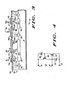
- FIG. 3 there is shown IC 10 in cross-sectional view illustrating the Schottky diode protection clamp circuit of the preferred embodiment which inhibits S CR 12 from being rendered conductive as aforedescribed. It is to be understood that the same reference numerals used in FIG. 2 are utilized in FIG. 3 to identify corresponding elements. Additional P+ region 84 is formed in epitaxial region 64 to which metal deposition layer 74 is contacted. Similarly, additional P+ region 86 is formed in tub 66 to which metal layer 80 is contacted. Thus, a pair of Schottky diodes are formed across the base-emitter junctions of parasitic transistors 46 and 48 as illustrated in FIG. 4.
- Schottky diodes 88 and 90 clamp the base-emitter junctions of transistors 48 and 46 respectively. These diodes restrict either transistor or parasitic SCR 12 from entering the active region of operation. Therefore, the current spike that can otherwise be generated in IC 10 of FIGs. 1 and 2 is inhibited by the Schottky diode clamp protection circuit. This is due to the fact that diode 88 serves to clamp the epi voltage of tub 64 to a value: where V N is the input voltage present at pin 14 and is the forward voltage drop of a Schottky diode. This will be transparant during normal circuit operation, and will prevent active operation of transistor 48 when IC 10 is inadvertently operated with substrate 50 not grounded as previously described. Diode 90 is reverse biased during normal operation, but will clamp the base-emitter junction of transistor 46 to ⁇ when the substrate is left floating.
Landscapes
- Semiconductor Integrated Circuits (AREA)
- Bipolar Integrated Circuits (AREA)
- Thyristor Switches And Gates (AREA)
Applications Claiming Priority (2)
| Application Number | Priority Date | Filing Date | Title |
|---|---|---|---|
| US56815684A | 1984-01-04 | 1984-01-04 | |
| US568156 | 1984-01-04 |
Publications (2)
| Publication Number | Publication Date |
|---|---|
| EP0149065A2 true EP0149065A2 (de) | 1985-07-24 |
| EP0149065A3 EP0149065A3 (de) | 1987-08-05 |
Family
ID=24270128
Family Applications (1)
| Application Number | Title | Priority Date | Filing Date |
|---|---|---|---|
| EP84114209A Withdrawn EP0149065A3 (de) | 1984-01-04 | 1984-11-24 | Schutz-Blockierschaltung für eine monolitische Schaltung zur Verhinderung von Spitzenströmen |
Country Status (2)
| Country | Link |
|---|---|
| EP (1) | EP0149065A3 (de) |
| JP (1) | JPS60160158A (de) |
Cited By (4)
| Publication number | Priority date | Publication date | Assignee | Title |
|---|---|---|---|---|
| US5341114A (en) * | 1990-11-02 | 1994-08-23 | Ail Systems, Inc. | Integrated limiter and amplifying devices |
| EP0730299A1 (de) * | 1995-02-28 | 1996-09-04 | Co.Ri.M.Me. | Schaltkreis zum Vorspannen von epitaxialen Gebieten |
| EP0809293B1 (de) * | 1996-05-21 | 2001-08-29 | Co.Ri.M.Me. Consorzio Per La Ricerca Sulla Microelettronica Nel Mezzogiorno | Leistungshalbleiterstruktur mit einem durch den Vertikaltransistor gesteuerten Lateraltransistor |
| CN114121933A (zh) * | 2020-09-01 | 2022-03-01 | 广东美的白色家电技术创新中心有限公司 | 集成电路及家用电器 |
Family Cites Families (2)
| Publication number | Priority date | Publication date | Assignee | Title |
|---|---|---|---|---|
| US3816762A (en) * | 1973-01-02 | 1974-06-11 | Fairchild Camera Instr Co | Noise suppression circuit |
| US3940785A (en) * | 1974-05-06 | 1976-02-24 | Sprague Electric Company | Semiconductor I.C. with protection against reversed power supply |
-
1984
- 1984-11-24 EP EP84114209A patent/EP0149065A3/de not_active Withdrawn
- 1984-12-19 JP JP59268208A patent/JPS60160158A/ja active Pending
Cited By (8)
| Publication number | Priority date | Publication date | Assignee | Title |
|---|---|---|---|---|
| US5341114A (en) * | 1990-11-02 | 1994-08-23 | Ail Systems, Inc. | Integrated limiter and amplifying devices |
| GB2284503A (en) * | 1990-11-02 | 1995-06-07 | Ail Systems Inc | Integrated limiter and amplifying devices |
| US5445985A (en) * | 1990-11-02 | 1995-08-29 | Ail Systems, Inc. | Method of forming integrated limiter and amplifying devices |
| GB2284503B (en) * | 1990-11-02 | 1995-10-25 | Ail Systems Inc | Integrated limiter and amplifying devices |
| EP0730299A1 (de) * | 1995-02-28 | 1996-09-04 | Co.Ri.M.Me. | Schaltkreis zum Vorspannen von epitaxialen Gebieten |
| US5796292A (en) * | 1995-02-28 | 1998-08-18 | Consorzio Per La Ricerca Sulla Microelettronica Nel Mezzogiorno | Circuit for biasing epitaxial regions with a bias voltage that is not lower than ground reference despite power supply disturbation |
| EP0809293B1 (de) * | 1996-05-21 | 2001-08-29 | Co.Ri.M.Me. Consorzio Per La Ricerca Sulla Microelettronica Nel Mezzogiorno | Leistungshalbleiterstruktur mit einem durch den Vertikaltransistor gesteuerten Lateraltransistor |
| CN114121933A (zh) * | 2020-09-01 | 2022-03-01 | 广东美的白色家电技术创新中心有限公司 | 集成电路及家用电器 |
Also Published As
| Publication number | Publication date |
|---|---|
| EP0149065A3 (de) | 1987-08-05 |
| JPS60160158A (ja) | 1985-08-21 |
Similar Documents
| Publication | Publication Date | Title |
|---|---|---|
| US6236087B1 (en) | SCR cell for electrical overstress protection of electronic circuits | |
| US5212618A (en) | Electrostatic discharge clamp using vertical NPN transistor | |
| US5473169A (en) | Complementary-SCR electrostatic discharge protection circuit | |
| KR970004453B1 (ko) | 집적회로 보호장치 및 제조방법 | |
| US6621126B2 (en) | Multifinger silicon controlled rectifier structure for electrostatic discharge protection | |
| US5646433A (en) | Pad protection diode structure | |
| KR0159451B1 (ko) | 반도체장치의 보호회로 | |
| US3881179A (en) | Zener diode structure having three terminals | |
| US5751525A (en) | EOS/ESD Protection circuit for an integrated circuit with operating/test voltages exceeding power supply rail voltages | |
| US6645820B1 (en) | Polycrystalline silicon diode string for ESD protection of different power supply connections | |
| KR100311578B1 (ko) | 반도체장치 | |
| IL29307A (en) | Voltage distribution system for integrated circuits | |
| US4543593A (en) | Semiconductor protective device | |
| US4806999A (en) | Area efficient input protection | |
| JPH07130963A (ja) | モノリシック集積回路と保護装置 | |
| KR100334381B1 (ko) | 유도성부하소자용집적드라이버회로 | |
| EP0703621A2 (de) | Elektrostatische Entladungsschutzanordnung für MOS-ingegrierte Schaltungen | |
| US5661332A (en) | Semiconductor diffused resistor | |
| KR100194496B1 (ko) | 반도체 장치 | |
| US4599631A (en) | Semiconductor apparatus having a zener diode integral with a resistor-transistor combination | |
| EP0822596A2 (de) | ESD-Schutzschaltung | |
| EP0149065A2 (de) | Schutz-Blockierschaltung für eine monolitische Schaltung zur Verhinderung von Spitzenströmen | |
| US4860083A (en) | Semiconductor integrated circuit | |
| US5336920A (en) | Buried avalanche diode having laterally adjacent semiconductor layers | |
| EP0202646B1 (de) | Eingangsschutzanordnung |
Legal Events
| Date | Code | Title | Description |
|---|---|---|---|
| PUAI | Public reference made under article 153(3) epc to a published international application that has entered the european phase |
Free format text: ORIGINAL CODE: 0009012 |
|
| AK | Designated contracting states |
Designated state(s): DE FR GB IT NL |
|
| PUAL | Search report despatched |
Free format text: ORIGINAL CODE: 0009013 |
|
| RHK1 | Main classification (correction) |
Ipc: H01L 27/06 |
|
| AK | Designated contracting states |
Kind code of ref document: A3 Designated state(s): DE FR GB IT NL |
|
| STAA | Information on the status of an ep patent application or granted ep patent |
Free format text: STATUS: THE APPLICATION IS DEEMED TO BE WITHDRAWN |
|
| 18D | Application deemed to be withdrawn |
Effective date: 19861201 |
|
| RIN1 | Information on inventor provided before grant (corrected) |
Inventor name: DANIELS, PAUL JACKSON Inventor name: STANLEY, MICHAEL EDWARD |