EP0097772A2 - Struktur mit monokristallinem Substrat als Träger für eine Halbleiterschicht für eine Anordnung - Google Patents
Struktur mit monokristallinem Substrat als Träger für eine Halbleiterschicht für eine Anordnung Download PDFInfo
- Publication number
- EP0097772A2 EP0097772A2 EP83103163A EP83103163A EP0097772A2 EP 0097772 A2 EP0097772 A2 EP 0097772A2 EP 83103163 A EP83103163 A EP 83103163A EP 83103163 A EP83103163 A EP 83103163A EP 0097772 A2 EP0097772 A2 EP 0097772A2
- Authority
- EP
- European Patent Office
- Prior art keywords
- layer
- substrate
- gaalas
- device layer
- gaas
- Prior art date
- Legal status (The legal status is an assumption and is not a legal conclusion. Google has not performed a legal analysis and makes no representation as to the accuracy of the status listed.)
- Granted
Links
Images
Classifications
-
- H—ELECTRICITY
- H10—SEMICONDUCTOR DEVICES; ELECTRIC SOLID-STATE DEVICES NOT OTHERWISE PROVIDED FOR
- H10H—INORGANIC LIGHT-EMITTING SEMICONDUCTOR DEVICES HAVING POTENTIAL BARRIERS
- H10H20/00—Individual inorganic light-emitting semiconductor devices having potential barriers, e.g. light-emitting diodes [LED]
- H10H20/01—Manufacture or treatment
- H10H20/011—Manufacture or treatment of bodies, e.g. forming semiconductor layers
- H10H20/013—Manufacture or treatment of bodies, e.g. forming semiconductor layers having light-emitting regions comprising only Group III-V materials
- H10H20/0133—Manufacture or treatment of bodies, e.g. forming semiconductor layers having light-emitting regions comprising only Group III-V materials with a substrate not being Group III-V materials
-
- H—ELECTRICITY
- H10—SEMICONDUCTOR DEVICES; ELECTRIC SOLID-STATE DEVICES NOT OTHERWISE PROVIDED FOR
- H10F—INORGANIC SEMICONDUCTOR DEVICES SENSITIVE TO INFRARED RADIATION, LIGHT, ELECTROMAGNETIC RADIATION OF SHORTER WAVELENGTH OR CORPUSCULAR RADIATION
- H10F30/00—Individual radiation-sensitive semiconductor devices in which radiation controls the flow of current through the devices, e.g. photodetectors
- H10F30/20—Individual radiation-sensitive semiconductor devices in which radiation controls the flow of current through the devices, e.g. photodetectors the devices having potential barriers, e.g. phototransistors
- H10F30/21—Individual radiation-sensitive semiconductor devices in which radiation controls the flow of current through the devices, e.g. photodetectors the devices having potential barriers, e.g. phototransistors the devices being sensitive to infrared, visible or ultraviolet radiation
- H10F30/22—Individual radiation-sensitive semiconductor devices in which radiation controls the flow of current through the devices, e.g. photodetectors the devices having potential barriers, e.g. phototransistors the devices being sensitive to infrared, visible or ultraviolet radiation the devices having only one potential barrier, e.g. photodiodes
- H10F30/227—Individual radiation-sensitive semiconductor devices in which radiation controls the flow of current through the devices, e.g. photodetectors the devices having potential barriers, e.g. phototransistors the devices being sensitive to infrared, visible or ultraviolet radiation the devices having only one potential barrier, e.g. photodiodes the potential barrier being a Schottky barrier
-
- H—ELECTRICITY
- H10—SEMICONDUCTOR DEVICES; ELECTRIC SOLID-STATE DEVICES NOT OTHERWISE PROVIDED FOR
- H10F—INORGANIC SEMICONDUCTOR DEVICES SENSITIVE TO INFRARED RADIATION, LIGHT, ELECTROMAGNETIC RADIATION OF SHORTER WAVELENGTH OR CORPUSCULAR RADIATION
- H10F71/00—Manufacture or treatment of devices covered by this subclass
- H10F71/127—The active layers comprising only Group III-V materials, e.g. GaAs or InP
- H10F71/1272—The active layers comprising only Group III-V materials, e.g. GaAs or InP comprising at least three elements, e.g. GaAlAs or InGaAsP
-
- H—ELECTRICITY
- H10—SEMICONDUCTOR DEVICES; ELECTRIC SOLID-STATE DEVICES NOT OTHERWISE PROVIDED FOR
- H10H—INORGANIC LIGHT-EMITTING SEMICONDUCTOR DEVICES HAVING POTENTIAL BARRIERS
- H10H20/00—Individual inorganic light-emitting semiconductor devices having potential barriers, e.g. light-emitting diodes [LED]
- H10H20/01—Manufacture or treatment
- H10H20/011—Manufacture or treatment of bodies, e.g. forming semiconductor layers
- H10H20/013—Manufacture or treatment of bodies, e.g. forming semiconductor layers having light-emitting regions comprising only Group III-V materials
-
- H10P14/2901—
-
- H10P14/2921—
-
- H10P14/3211—
-
- H10P14/3221—
-
- H10P14/3248—
-
- H10P14/3251—
-
- H10P14/3421—
-
- H10P14/24—
-
- Y—GENERAL TAGGING OF NEW TECHNOLOGICAL DEVELOPMENTS; GENERAL TAGGING OF CROSS-SECTIONAL TECHNOLOGIES SPANNING OVER SEVERAL SECTIONS OF THE IPC; TECHNICAL SUBJECTS COVERED BY FORMER USPC CROSS-REFERENCE ART COLLECTIONS [XRACs] AND DIGESTS
- Y02—TECHNOLOGIES OR APPLICATIONS FOR MITIGATION OR ADAPTATION AGAINST CLIMATE CHANGE
- Y02E—REDUCTION OF GREENHOUSE GAS [GHG] EMISSIONS, RELATED TO ENERGY GENERATION, TRANSMISSION OR DISTRIBUTION
- Y02E10/00—Energy generation through renewable energy sources
- Y02E10/50—Photovoltaic [PV] energy
- Y02E10/544—Solar cells from Group III-V materials
-
- Y—GENERAL TAGGING OF NEW TECHNOLOGICAL DEVELOPMENTS; GENERAL TAGGING OF CROSS-SECTIONAL TECHNOLOGIES SPANNING OVER SEVERAL SECTIONS OF THE IPC; TECHNICAL SUBJECTS COVERED BY FORMER USPC CROSS-REFERENCE ART COLLECTIONS [XRACs] AND DIGESTS
- Y02—TECHNOLOGIES OR APPLICATIONS FOR MITIGATION OR ADAPTATION AGAINST CLIMATE CHANGE
- Y02P—CLIMATE CHANGE MITIGATION TECHNOLOGIES IN THE PRODUCTION OR PROCESSING OF GOODS
- Y02P70/00—Climate change mitigation technologies in the production process for final industrial or consumer products
- Y02P70/50—Manufacturing or production processes characterised by the final manufactured product
Definitions
- This invention relates to structures comprising a monocrystalline substrate supporting a device layer of semiconductor material.
- Intermetallic semiconductor material crystals of more than one element such as GaAs and GaAlAs have a number of properties useful in integrated circuit structures but to take full advantage of those properties it is necessary to build the integrated circuit structure in a thin layer with properties that produce device advantages supported by a substrate with different properties. It is desirable that the properties of the substrate have minimal effect on the properties of the device layer.
- One integrated circuit structure in use in the art involves making the integrated circuit in a layer of GaAs on a substrate of high resistivity or semi-insulating GaAs.
- impurities in the doping that renders the substrate semi-insulating have a detrimental effect on device performance.
- Another integrated circuit structure developed in the art involves the making and the isolating of integrated circuits in a layer of GaAs on a substrate of A1 2 0 3 as described in Metallurgical Transactions Vol. 1, March 1970, pages 623-628 and in Journal of Applied Physics Vol. 42, No. 6, May 1971, pages 2519-2527.
- problems are encountered with crystal defects at the GaAs-Al 0 interface.
- Still another semiconductor structure involves selectively doped very thin layers of different semiconductor materials.
- This structure is known as a high electron mobility transistor (HEMT) and is described in the Japanese Journal of Applied Physics, Vol. 19, No. 5, May 1980, pp. L225 to L227. This structure places very stringent requirements on the quality of the substrate and the semiconductor material adjacent the device.
- HEMT high electron mobility transistor
- a structure comprising a monocrystalline substrate supporting a device layer of semiconductor material in which semiconductor devices can be formed, is characterised, according to the invention, by the inclusion of an intermediate, lattice accommodating epitaxial layer of G aAlAs positioned between the monocrystalline substrate and said device layer.
- the invention may be viewed as an intermediate manufacturing product which may be employed in a variety of ways to achieve integrated circuit structure benefits.
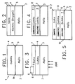
- the structure 1 has a monocrystalline insulating substrate 2 which is joined at a line of demarcation 3 with an epitaxial layer 4 of GaAlAs.
- the GaAlAs layer 4 is generally undoped but may contain conductivity type determining impurities in accordance with the properties desired to be imparted to the ultimate integrated circuit structure. Since GaAlAs may have varying quantities of Ga and Al usually described as Ga Al As where x varies from about 0.1 to 0.9 and the electrical and optical properties vary with x, much flexibility can be achieved.
- the GaAlAs intermediate layer 4 is epitaxial with the crystalline substrate 2 and provides a barrier to electrons, in a device layer which will be formed over the exposed surface of at least portions of the layer 4, from interacting with interface defects at the interface 3.
- the GaAlAs intermediate layer 4 also permits wide differences in resistance properties in the material chosen for the substrate 2 from affecting the properties of the integrated circuit devices.
- a thin layer 5 of Ge may be included in order to improve the lattice spacing transition from the spacing of the substrate 2 to that of the GaAlAs layer 4.
- the substrate 2 is of a crystalline material with crystal structure and lattice spacing compatible with epitaxial growth of the GaAlAs layer 4.
- the substrate may be of insulating material such as sapphire, spinel, ZnSe or conducting GaAs.
- the substrate may be chosen to impart a variety of properties such as resistance, optical transparency and thermal conductance. Where the substrate 2 is optically transparent and light transmission is employed as part of the application of the invention, the Ge layer 5 would not be used since it is optically opaque to the frequencies of most device materials such as GaAs and GaAlAs.
- the structure 1 may be employed in various types of integrated circuit structures as illustrated in FIGS. 2, 3, 4 and 5.
- the intermediate structure of FIG. 1 is provided with an epitaxial device layer 6 of GaAs in which an integrated circuit is to be formed.
- the layer 6 joins the GaAlAs layer 4 epitaxially at an interface 7.
- the region 4 and the region 6 may be provided with oxygen in the few parts per million range. This causes the GaAlAs layer 4 to be highly insulating. The oxygen will also give the GaAs layer 6 high resistivity so that processing operations such as ion implantation to produce arrays of field effect transistors may be employed.
- the addition of a 5 micron thickness layer 5 of Ge would permit a wider lattice spacing tolerance in the selection of the material for the substrate 2.
- the substrate 2 is made of the material A1 2 0 3
- the defects at the interface 3 may not, however, be a sufficient problem to justify adding the Ge layer 5 with the added processing complexity.
- an optically active device 8 such as a region of GaAs with a p-n junction 9 or a Schottky barrier is positioned in at least a portion of the surface of the region 6.
- a device actuating light signal can be introduced through a transparent substrate 2 of A1 2 0 3 and the intermediate region 4 to produce carriers in the device layer 6 to be collected through an external ohmic contact (not shown) to the device 8.
- Optical performance can be improved by providing a low recombination velocity condition well known in the photovoltaic cell art at the interface 7. It will be apparent that the Ge layer 5 would not be used in this structure since the Ge would operate to attenuate light of the wavelengths employed with GaAs.
- the GaAlAs region 4 is made insulating and is equipped with a conductive GaAlAs layer 11 epitaxially joined to the region 4 at an interface 12.
- the layer 11 may be formed by the techniques of ion implantation, diffusion or vapor growth.
- a layer 13 of undoped GaAs is added to the structure of FIG. 4 where the GaAs layer 13 and the conductive GaAlAs layer 11 are at least 0.06 micrometers thick to provide an improved structure for the high electron mobility transistor (HEMT) device currently receiving attention in the art.
- HEMT high electron mobility transistor
- the layers are so thin that advantage can be taken of the spatial separation between electrons and their parent donor impurities.
- Misfit dislocations at the interface 3 will be passive in structures employing the invention as opposed to the conditions present in the "silicon on sapphire" type structures common in the silicon industry. Further imperfections originating at the interface 3 will propagate in the intermediate layer 4 but will not grow perpendicular to the interfaces 7 and 12 between the intermediate and device layers and when they reach the device layers 6 and 11 they will propagate parallel to the interfaces 7 and 12 resulting in a higher quality device layer.
- a preferred embodiment of the invention is a structure similar to FIG. 2 with a substrate 2 of A1 2 0 3 of sufficient thickness for handling.
- a 2 to 20 micron thick layer 4 of Gao,5x A1 1-0.5x As is epitaxially grown thereon, through the technique of the decomposition of vapors of trimethyl aluminum, trimethyl gallium and arsine.
- This is followed by a layer of GaAs of at least 0.1 microns thickness in which no Al- containing vapor is provided in the growth with the Ga source and the As source.
- the GaAs layer 6 In order for the GaAs layer 6 to be useful for active devices, it should have an average carrier mobility of the order of 5,000 centimetres per volt second and have a doping concentration between 10 15 and 10 16 atoms per cc.
- the Ge layer 5 is employed, it would be grown first on the A O2 O 3 to a depth of around 5 microns followed by the GaAlAs described.
- the GaAs layer 6 could be 2 to 20 microns thick and oxygen doped to give it high resistivity and a technique such as ion implantation used to form the active device region.
Landscapes
- Recrystallisation Techniques (AREA)
- Junction Field-Effect Transistors (AREA)
- Bipolar Integrated Circuits (AREA)
Applications Claiming Priority (2)
| Application Number | Priority Date | Filing Date | Title |
|---|---|---|---|
| US393951 | 1982-06-30 | ||
| US06/393,951 US4482906A (en) | 1982-06-30 | 1982-06-30 | Gallium aluminum arsenide integrated circuit structure using germanium |
Publications (3)
| Publication Number | Publication Date |
|---|---|
| EP0097772A2 true EP0097772A2 (de) | 1984-01-11 |
| EP0097772A3 EP0097772A3 (en) | 1986-06-04 |
| EP0097772B1 EP0097772B1 (de) | 1989-06-07 |
Family
ID=23556905
Family Applications (1)
| Application Number | Title | Priority Date | Filing Date |
|---|---|---|---|
| EP83103163A Expired EP0097772B1 (de) | 1982-06-30 | 1983-03-30 | Struktur mit monokristallinem Substrat als Träger für eine Halbleiterschicht für eine Anordnung |
Country Status (4)
| Country | Link |
|---|---|
| US (1) | US4482906A (de) |
| EP (1) | EP0097772B1 (de) |
| JP (1) | JPS5946068A (de) |
| DE (1) | DE3380046D1 (de) |
Families Citing this family (43)
| Publication number | Priority date | Publication date | Assignee | Title |
|---|---|---|---|---|
| US4710478A (en) * | 1985-05-20 | 1987-12-01 | United States Of America As Represented By The Secretary Of The Navy | Method for making germanium/gallium arsenide high mobility complementary logic transistors |
| US4860067A (en) * | 1986-06-20 | 1989-08-22 | International Business Machines Corporation | Semiconductor heterostructure adapted for low temperature operation |
| US4872040A (en) * | 1987-04-23 | 1989-10-03 | International Business Machines Corporation | Self-aligned heterojunction transistor |
| US4981807A (en) * | 1988-10-31 | 1991-01-01 | International Business Machines Corporation | Process for fabricating complementary vertical transistor memory cell |
| US5448084A (en) * | 1991-05-24 | 1995-09-05 | Raytheon Company | Field effect transistors on spinel substrates |
| JP3681236B2 (ja) * | 1996-10-28 | 2005-08-10 | 沖電気工業株式会社 | 半導体装置 |
| US6693033B2 (en) | 2000-02-10 | 2004-02-17 | Motorola, Inc. | Method of removing an amorphous oxide from a monocrystalline surface |
| US6392257B1 (en) | 2000-02-10 | 2002-05-21 | Motorola Inc. | Semiconductor structure, semiconductor device, communicating device, integrated circuit, and process for fabricating the same |
| JP2004503920A (ja) | 2000-05-31 | 2004-02-05 | モトローラ・インコーポレイテッド | 半導体デバイスおよび該半導体デバイスを製造する方法 |
| US6427066B1 (en) | 2000-06-30 | 2002-07-30 | Motorola, Inc. | Apparatus and method for effecting communications among a plurality of remote stations |
| US6501973B1 (en) | 2000-06-30 | 2002-12-31 | Motorola, Inc. | Apparatus and method for measuring selected physical condition of an animate subject |
| US6477285B1 (en) | 2000-06-30 | 2002-11-05 | Motorola, Inc. | Integrated circuits with optical signal propagation |
| US6410941B1 (en) | 2000-06-30 | 2002-06-25 | Motorola, Inc. | Reconfigurable systems using hybrid integrated circuits with optical ports |
| WO2002009187A2 (en) | 2000-07-24 | 2002-01-31 | Motorola, Inc. | Heterojunction tunneling diodes and process for fabricating same |
| US6555946B1 (en) | 2000-07-24 | 2003-04-29 | Motorola, Inc. | Acoustic wave device and process for forming the same |
| US6638838B1 (en) * | 2000-10-02 | 2003-10-28 | Motorola, Inc. | Semiconductor structure including a partially annealed layer and method of forming the same |
| US6583034B2 (en) | 2000-11-22 | 2003-06-24 | Motorola, Inc. | Semiconductor structure including a compliant substrate having a graded monocrystalline layer and methods for fabricating the structure and semiconductor devices including the structure |
| US6563118B2 (en) | 2000-12-08 | 2003-05-13 | Motorola, Inc. | Pyroelectric device on a monocrystalline semiconductor substrate and process for fabricating same |
| US20020096683A1 (en) | 2001-01-19 | 2002-07-25 | Motorola, Inc. | Structure and method for fabricating GaN devices utilizing the formation of a compliant substrate |
| US6673646B2 (en) | 2001-02-28 | 2004-01-06 | Motorola, Inc. | Growth of compound semiconductor structures on patterned oxide films and process for fabricating same |
| US7046719B2 (en) | 2001-03-08 | 2006-05-16 | Motorola, Inc. | Soft handoff between cellular systems employing different encoding rates |
| WO2002082551A1 (en) | 2001-04-02 | 2002-10-17 | Motorola, Inc. | A semiconductor structure exhibiting reduced leakage current |
| US6709989B2 (en) | 2001-06-21 | 2004-03-23 | Motorola, Inc. | Method for fabricating a semiconductor structure including a metal oxide interface with silicon |
| US6992321B2 (en) | 2001-07-13 | 2006-01-31 | Motorola, Inc. | Structure and method for fabricating semiconductor structures and devices utilizing piezoelectric materials |
| US6646293B2 (en) | 2001-07-18 | 2003-11-11 | Motorola, Inc. | Structure for fabricating high electron mobility transistors utilizing the formation of complaint substrates |
| US6693298B2 (en) | 2001-07-20 | 2004-02-17 | Motorola, Inc. | Structure and method for fabricating epitaxial semiconductor on insulator (SOI) structures and devices utilizing the formation of a compliant substrate for materials used to form same |
| US7019332B2 (en) | 2001-07-20 | 2006-03-28 | Freescale Semiconductor, Inc. | Fabrication of a wavelength locker within a semiconductor structure |
| US6472694B1 (en) | 2001-07-23 | 2002-10-29 | Motorola, Inc. | Microprocessor structure having a compound semiconductor layer |
| US6855992B2 (en) | 2001-07-24 | 2005-02-15 | Motorola Inc. | Structure and method for fabricating configurable transistor devices utilizing the formation of a compliant substrate for materials used to form the same |
| US6585424B2 (en) | 2001-07-25 | 2003-07-01 | Motorola, Inc. | Structure and method for fabricating an electro-rheological lens |
| US6594414B2 (en) | 2001-07-25 | 2003-07-15 | Motorola, Inc. | Structure and method of fabrication for an optical switch |
| US6667196B2 (en) | 2001-07-25 | 2003-12-23 | Motorola, Inc. | Method for real-time monitoring and controlling perovskite oxide film growth and semiconductor structure formed using the method |
| US6639249B2 (en) | 2001-08-06 | 2003-10-28 | Motorola, Inc. | Structure and method for fabrication for a solid-state lighting device |
| US6462360B1 (en) | 2001-08-06 | 2002-10-08 | Motorola, Inc. | Integrated gallium arsenide communications systems |
| US6589856B2 (en) | 2001-08-06 | 2003-07-08 | Motorola, Inc. | Method and apparatus for controlling anti-phase domains in semiconductor structures and devices |
| US20030034491A1 (en) | 2001-08-14 | 2003-02-20 | Motorola, Inc. | Structure and method for fabricating semiconductor structures and devices for detecting an object |
| US6673667B2 (en) | 2001-08-15 | 2004-01-06 | Motorola, Inc. | Method for manufacturing a substantially integral monolithic apparatus including a plurality of semiconductor materials |
| US20030071327A1 (en) | 2001-10-17 | 2003-04-17 | Motorola, Inc. | Method and apparatus utilizing monocrystalline insulator |
| US6916717B2 (en) | 2002-05-03 | 2005-07-12 | Motorola, Inc. | Method for growing a monocrystalline oxide layer and for fabricating a semiconductor device on a monocrystalline substrate |
| US7169619B2 (en) | 2002-11-19 | 2007-01-30 | Freescale Semiconductor, Inc. | Method for fabricating semiconductor structures on vicinal substrates using a low temperature, low pressure, alkaline earth metal-rich process |
| US6885065B2 (en) | 2002-11-20 | 2005-04-26 | Freescale Semiconductor, Inc. | Ferromagnetic semiconductor structure and method for forming the same |
| US6965128B2 (en) | 2003-02-03 | 2005-11-15 | Freescale Semiconductor, Inc. | Structure and method for fabricating semiconductor microresonator devices |
| US7020374B2 (en) | 2003-02-03 | 2006-03-28 | Freescale Semiconductor, Inc. | Optical waveguide structure and method for fabricating the same |
Family Cites Families (16)
| Publication number | Priority date | Publication date | Assignee | Title |
|---|---|---|---|---|
| GB1319560A (en) * | 1970-06-04 | 1973-06-06 | North American Rockwell | Epitaxial composite and method of making |
| GB1508799A (en) * | 1974-09-26 | 1978-04-26 | Standard Telephones Cables Ltd | Light emissive semiconductor device |
| US3954534A (en) * | 1974-10-29 | 1976-05-04 | Xerox Corporation | Method of forming light emitting diode array with dome geometry |
| US3963536A (en) * | 1974-11-18 | 1976-06-15 | Rca Corporation | Method of making electroluminescent semiconductor devices |
| US4035829A (en) * | 1975-01-13 | 1977-07-12 | Rca Corporation | Semiconductor device and method of electrically isolating circuit components thereon |
| US4075651A (en) * | 1976-03-29 | 1978-02-21 | Varian Associates, Inc. | High speed fet employing ternary and quarternary iii-v active layers |
| US4157556A (en) * | 1977-01-06 | 1979-06-05 | Varian Associates, Inc. | Heterojunction confinement field effect transistor |
| FR2386903A1 (fr) * | 1977-04-08 | 1978-11-03 | Thomson Csf | Transistor a effet de champ sur support a grande bande interdite |
| US4160261A (en) * | 1978-01-13 | 1979-07-03 | Bell Telephone Laboratories, Incorporated | Mis heterojunction structures |
| US4194935A (en) * | 1978-04-24 | 1980-03-25 | Bell Telephone Laboratories, Incorporated | Method of making high mobility multilayered heterojunction devices employing modulated doping |
| US4212020A (en) * | 1978-07-21 | 1980-07-08 | California Institute Of Technology | Solid state electro-optical devices on a semi-insulating substrate |
| US4236166A (en) * | 1979-07-05 | 1980-11-25 | Bell Telephone Laboratories, Incorporated | Vertical field effect transistor |
| FR2462027A1 (fr) * | 1979-07-20 | 1981-02-06 | Labo Electronique Physique | Dispositif semi-conducteur comportant une couche tampon isolante |
| US4346394A (en) * | 1980-03-24 | 1982-08-24 | Hughes Aircraft Company | Gallium arsenide burrus FET structure for optical detection |
| US4370510A (en) * | 1980-09-26 | 1983-01-25 | California Institute Of Technology | Gallium arsenide single crystal solar cell structure and method of making |
| US4385198A (en) * | 1981-07-08 | 1983-05-24 | The United States Of America As Represented By The Secretary Of The Air Force | Gallium arsenide-germanium heteroface junction device |
-
1982
- 1982-06-30 US US06/393,951 patent/US4482906A/en not_active Expired - Fee Related
-
1983
- 1983-03-30 DE DE8383103163T patent/DE3380046D1/de not_active Expired
- 1983-03-30 EP EP83103163A patent/EP0097772B1/de not_active Expired
- 1983-04-14 JP JP58064653A patent/JPS5946068A/ja active Pending
Also Published As
| Publication number | Publication date |
|---|---|
| JPS5946068A (ja) | 1984-03-15 |
| US4482906A (en) | 1984-11-13 |
| DE3380046D1 (en) | 1989-07-13 |
| EP0097772A3 (en) | 1986-06-04 |
| EP0097772B1 (de) | 1989-06-07 |
Similar Documents
| Publication | Publication Date | Title |
|---|---|---|
| EP0097772A2 (de) | Struktur mit monokristallinem Substrat als Träger für eine Halbleiterschicht für eine Anordnung | |
| Bean | Strained-layer epitaxy of germanium-silicon alloys | |
| US4885614A (en) | Semiconductor device with crystalline silicon-germanium-carbon alloy | |
| US5442191A (en) | Isotopically enriched semiconductor devices | |
| US5144379A (en) | Semiconductor device having a group iii-v epitaxial semiconductor layer on a substrate | |
| US4769341A (en) | Method of fabricating non-silicon materials on silicon substrate using an alloy of Sb and Group IV semiconductors | |
| US20020070416A1 (en) | Current isolating epitaxial buffer layers for high voltage photodiode array | |
| US5599389A (en) | Compound semiconductor and method of manufacturing the same | |
| US4697202A (en) | Integrated circuit having dislocation free substrate | |
| US5229625A (en) | Schottky barrier gate type field effect transistor | |
| US5562770A (en) | Semiconductor manufacturing process for low dislocation defects | |
| US6287946B1 (en) | Fabrication of low resistance, non-alloyed, ohmic contacts to InP using non-stoichiometric InP layers | |
| EP0180457B1 (de) | Halbleiteranordnung mit einer integrierten Schaltung und Verfahren zu deren Herstellung | |
| US5309003A (en) | Article comprising a real space transfer semiconductor device, and method of making the article | |
| US4791072A (en) | Method for making a complementary device containing MODFET | |
| EP0205164B1 (de) | Struktur einer Halbleiteranordnung | |
| US4872040A (en) | Self-aligned heterojunction transistor | |
| EP0853821B1 (de) | Halbleiterdiode mit unterdrückung von auger-generationsprozessen | |
| US5024967A (en) | Doping procedures for semiconductor devices | |
| US5183776A (en) | Heteroepitaxy by growth of thermally strained homojunction superlattice buffer layers | |
| Thorsen et al. | Material and device properties of heteroepitaxial GaAs on BeO | |
| KR950001620B1 (ko) | 규소저매늄/저매늄 완충층을 이용한 규소기판상의 갈륨비소 박막성장방법 | |
| USRE38582E1 (en) | Semiconductor diode with suppression of auger generation processes | |
| JPH0289325A (ja) | 化合物半導体の構造体及びその形成方法 | |
| KR920006854B1 (ko) | 화합물 반도체소자 및 그 제조방법 |
Legal Events
| Date | Code | Title | Description |
|---|---|---|---|
| PUAI | Public reference made under article 153(3) epc to a published international application that has entered the european phase |
Free format text: ORIGINAL CODE: 0009012 |
|
| AK | Designated contracting states |
Designated state(s): DE FR GB |
|
| 17P | Request for examination filed |
Effective date: 19840426 |
|
| PUAL | Search report despatched |
Free format text: ORIGINAL CODE: 0009013 |
|
| AK | Designated contracting states |
Kind code of ref document: A3 Designated state(s): DE FR GB |
|
| 17Q | First examination report despatched |
Effective date: 19870918 |
|
| GRAA | (expected) grant |
Free format text: ORIGINAL CODE: 0009210 |
|
| AK | Designated contracting states |
Kind code of ref document: B1 Designated state(s): DE FR GB |
|
| REF | Corresponds to: |
Ref document number: 3380046 Country of ref document: DE Date of ref document: 19890713 |
|
| ET | Fr: translation filed | ||
| PLBE | No opposition filed within time limit |
Free format text: ORIGINAL CODE: 0009261 |
|
| STAA | Information on the status of an ep patent application or granted ep patent |
Free format text: STATUS: NO OPPOSITION FILED WITHIN TIME LIMIT |
|
| 26N | No opposition filed | ||
| PGFP | Annual fee paid to national office [announced via postgrant information from national office to epo] |
Ref country code: GB Payment date: 19920210 Year of fee payment: 10 |
|
| PGFP | Annual fee paid to national office [announced via postgrant information from national office to epo] |
Ref country code: FR Payment date: 19920227 Year of fee payment: 10 |
|
| PGFP | Annual fee paid to national office [announced via postgrant information from national office to epo] |
Ref country code: DE Payment date: 19920321 Year of fee payment: 10 |
|
| PG25 | Lapsed in a contracting state [announced via postgrant information from national office to epo] |
Ref country code: GB Effective date: 19930330 |
|
| GBPC | Gb: european patent ceased through non-payment of renewal fee |
Effective date: 19930330 |
|
| PG25 | Lapsed in a contracting state [announced via postgrant information from national office to epo] |
Ref country code: FR Effective date: 19931130 |
|
| PG25 | Lapsed in a contracting state [announced via postgrant information from national office to epo] |
Ref country code: DE Effective date: 19931201 |
|
| REG | Reference to a national code |
Ref country code: FR Ref legal event code: ST |