EP0096165A2 - Appareil pour diviser les éléments d'un champ de Galois - Google Patents
Appareil pour diviser les éléments d'un champ de Galois Download PDFInfo
- Publication number
- EP0096165A2 EP0096165A2 EP83102308A EP83102308A EP0096165A2 EP 0096165 A2 EP0096165 A2 EP 0096165A2 EP 83102308 A EP83102308 A EP 83102308A EP 83102308 A EP83102308 A EP 83102308A EP 0096165 A2 EP0096165 A2 EP 0096165A2
- Authority
- EP
- European Patent Office
- Prior art keywords
- sup
- data
- reciprocal
- shift register
- data representing
- Prior art date
- Legal status (The legal status is an assumption and is not a legal conclusion. Google has not performed a legal analysis and makes no representation as to the accuracy of the status listed.)
- Granted
Links
Images


Classifications
-
- G—PHYSICS
- G06—COMPUTING; CALCULATING OR COUNTING
- G06F—ELECTRIC DIGITAL DATA PROCESSING
- G06F7/00—Methods or arrangements for processing data by operating upon the order or content of the data handled
- G06F7/60—Methods or arrangements for performing computations using a digital non-denominational number representation, i.e. number representation without radix; Computing devices using combinations of denominational and non-denominational quantity representations, e.g. using difunction pulse trains, STEELE computers, phase computers
- G06F7/72—Methods or arrangements for performing computations using a digital non-denominational number representation, i.e. number representation without radix; Computing devices using combinations of denominational and non-denominational quantity representations, e.g. using difunction pulse trains, STEELE computers, phase computers using residue arithmetic
- G06F7/724—Finite field arithmetic
- G06F7/726—Inversion; Reciprocal calculation; Division of elements of a finite field
-
- G—PHYSICS
- G11—INFORMATION STORAGE
- G11B—INFORMATION STORAGE BASED ON RELATIVE MOVEMENT BETWEEN RECORD CARRIER AND TRANSDUCER
- G11B20/00—Signal processing not specific to the method of recording or reproducing; Circuits therefor
- G11B20/10—Digital recording or reproducing
- G11B20/18—Error detection or correction; Testing, e.g. of drop-outs
- G11B20/1806—Pulse code modulation systems for audio signals
- G11B20/1809—Pulse code modulation systems for audio signals by interleaving
-
- H—ELECTRICITY
- H03—ELECTRONIC CIRCUITRY
- H03M—CODING; DECODING; CODE CONVERSION IN GENERAL
- H03M13/00—Coding, decoding or code conversion, for error detection or error correction; Coding theory basic assumptions; Coding bounds; Error probability evaluation methods; Channel models; Simulation or testing of codes
- H03M13/03—Error detection or forward error correction by redundancy in data representation, i.e. code words containing more digits than the source words
- H03M13/05—Error detection or forward error correction by redundancy in data representation, i.e. code words containing more digits than the source words using block codes, i.e. a predetermined number of check bits joined to a predetermined number of information bits
- H03M13/13—Linear codes
- H03M13/15—Cyclic codes, i.e. cyclic shifts of codewords produce other codewords, e.g. codes defined by a generator polynomial, Bose-Chaudhuri-Hocquenghem [BCH] codes
-
- G—PHYSICS
- G06—COMPUTING; CALCULATING OR COUNTING
- G06F—ELECTRIC DIGITAL DATA PROCESSING
- G06F1/00—Details not covered by groups G06F3/00 - G06F13/00 and G06F21/00
- G06F1/02—Digital function generators
- G06F1/03—Digital function generators working, at least partly, by table look-up
- G06F1/0307—Logarithmic or exponential functions
Definitions
- the present invention relates to an apparatus for dividing the elements of a Galois field, which can effectively serve to decode an error correction code used in an optical DAD (digital audio disk) device using, for example, a CD (compact disk).
- an optical DAD digital audio disk
- CD compact disk
- cross-interleaved Reed Solomon codes are used as error correction codes.
- the cross-interleaved Reed Solomon code thus obtained can correct even a burst error.
- a Reed Solomon code can be decoded in the same way as is a BCH code, thereby performing an error correction.
- a Reed Solomon code consisting of k data symbols and (n-k) inspection symbols i.e., a code consisting of n symbols
- n symbols are the 2 m elements of a finite field called "Galois field GF(2 m )" which represents m binary bits.
- the generator polynomial g( x ) representing a Reed Solomon code used to correct an error t times is given by the following equation (1) or (2), where a is the origin element of the Galois field G F ( 2 m ) :
- the coefficients contained in polynomial E(x) are also contained in Galois field GF (2 m ).
- the error polynomial E(x) contains only terms which correspond to an error location and the value (i.e., size) of an error.
- E is the sum of errors at all error locations.
- Error location polynomial ⁇ (x) is given by: where e is the number of errors.
- the Reed Solomon code may decoded in the following method A or the following method B.
- Fig. 1 is a block diagram of a known data correcting system which is designed to decode Reed Solomon codes in the manner described above.
- Data to be corrected are supplied through an input terminal IN and will be corrected by a Reed Solomon code.
- the data are stored in a data buffer 11 and kept stored there until a code decoding (later described) is completed.
- the data are supplied also to a syndrome calculator 12.
- the calculator 12 calculates a syndrome based on the input data and the syndrome is then stored in a syndrome buffer 13.
- An OR gate is coupled to the output of the syndrome buffer 13. It generates an output signal which indicates whether or not an error exists in the syndrome supplied from the syndrome buffer 13.
- An output signal from the OR gate is supplied to an error location polynomial calculator 15.
- the calculator 15 finds the coefficients included in an error location polynomial o(x). Data representing the coefficients are fed to an error location calculator 16.
- the error location calculator 16 finds the root or roots of the error location polynomial. Data representing the root or roots are supplied from the calculator 16 to an error value calculator 17. From the input data the calculator 17 calculates an error value. The data representing the root or roots and the data representing the error value are used to correct the data from the data buffer 11.
- the calculators 12, 15, 16 and 17 of the data correcting system can detect elements which are "0" and can therefore perform algebraic operations such as addition, multiplication or division.
- the error location polynomial calculator 16 may have such a structure as shown in Fig. 2 and disclosed in U.S. Patent No. 4,142,174.
- the error location polynomial calculator 16 comprises a syndrome buffer 21, a working buffer 22, a sequence controller 23, a logarithm buffer 24 and an antilogarithm buffer 25.
- the syndrome buffer 21 is a random-access memory (RAM) for storing a syndrome Si which is m-bit data and which represents each element of a Galois field GF(2 m ).
- the working buffer 22 is a RAM for storing an interim result of an algebraic operation performed in finding the coefficients of the error location polynomial and for storing the final result of the algebraic operation.
- the working buffer 22 may store partial results that will be used in algebraic operations which follow the operations for calculating the coefficients of the error location polynomial.
- the sequence controller 23 defines the order in which algebraic operations will be performed. It supplies address signals to the syndrome buffer 21 and the working buffer 22, to thereby designate desired memory locations of these buffers 21 and 22 and to check and branch the results of algebraic operations so that the results may be used in the next algebraic operations.
- the logarithm buffer 24 is a ROM (read-only memory) storing a table of the logarithms of the elements of a Galois field GF(2 m ).
- the antilogarithm buffer 25 is also a ROM storing a table of the antilogarithms of the elements of a Galois field G F ( 2 m).
- the address of the logarithm buffer 24 is a binary code of element a i . Its entry is the logarithm of a to the base - that is, i. The entry at address i of the antilogarithm buffer 25 is a binary code of a i .
- eight coefficients ao to a 7 may be taken and can be represented as binary vectors. For example, they can be given by:
- the elements of the Galois field GF(2 8 ) other than these can be represented as binary vectors.
- the addresses 1 - 255 of the logarithm table are 8-bit binary vectors of elements a i. Entries corresponding to the addresses are binary notation of exponent i. In the antilogarithm table, exponent i is used as an address, and entries are binary vectors of a i .
- the former is supplied from A register 20 to an exclusive OR gate 27 and the latter is supplied from B register 26 to the exclusive OR gate 27.
- An exclusive logical sum of each bit of element a i and the corresponding bit of element aj is thus produced.
- the logical sum of elements a i and aj obtained by the exclusive OR gate 27 is transferred through C register 19 to the working buffer 22.
- the error location polynomial calculator of the known error correcting system must be provided with a logarithm buffer and an antilogarithm buffer. Without these buffers, the error location polynomial calculator could not perform multiplication or division. Both buffers, which are ROMs, need to have an enormously large memory capacity. This makes it difficult to manufacture the error location polynomial calculator in the form of an LSI. In order to make the calculator in the form of an LSI, the logarithm buffer and the antilogarithm buffer must be excluded from the calculator. In this case, the buffers having a large memory capacity have to be connected to the calculator.
- the known error location polynomial calculator is provided with two ROMs the total memory capacity of which amounts to 4080 bits.
- One of the ROMs stores a table of logarithms and the other ROM stores a table of antilogarithms. Since its error location polynomial calculator has two ROMs both with a large memory capacity, the error correcting system is inevitably complicated, and thus expensive.
- An object of the present invention is to provide an apparatus for dividing the elements of a Galois field, which has neither a logarithm buffer nor an antilogarithm buffer, both of which require a large memory capacity, and which therefore has a simple structure and can be manufactured at low cost.
- An apparatus divides one element a i of the Galois field GF(2 m ) by another element aj of the Galois field GF(2 m ), where a is a root of modulus polynomial F (x) .
- One of the elements of each group, which is located at a specific position, is sampled, and the data representing the reciprocal of the sampled element is stored in a reciprocal data memory means.
- the data representing the element ⁇ j of the Galois field GF(2 m ) is stored in a first linear shift register. This data is compared by comparator means with the reciprocal data which are stored in the reciprocal data memory means.
- the linear shift register is shifted a number of times until the data coincides with one of the reciprocal data so that the reciprocal data is read from the reciprocal data memory means.
- the number of times N that the linear shift register is shifted until one of the reciprocal data is read out is given as: 0 ⁇ N ⁇ n-1.
- the reciprocal data ⁇ -(j+N) read from the reciprocal data memory and the data representing element ⁇ i are used in multiplying ⁇ i by ⁇ -j by means of multiplication means including a second linear shift register and means for removing the a- N component.
- multiplication means including a second linear shift register and means for removing the a- N component.
- the elements of the Galois field GF(2 m ) are divided by using linear shift registers and multiplying the elements by means of these linear shift registers. This can reduce the memory capacity of the memory means for storing necessary reciprocal data, thus simplifying the structure of the apparatus and lowering the cost of the apparatus.
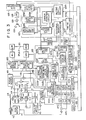
- the optical DAD device comprises a motor 111 for rotating a turntable 112.
- an optical disk 113 is mounted on the turntable 112 on the turntable 112 .
- the disk 113 has pits which correspond to digital audio signals (i.e. PCM codes) which have been EFM-modulated and interleaved.
- An optical pickup 114 emits a laser beam from a semiconductor laser 114a.
- the laser beam passes through a beam splitter 114b and is focused by an objective lens 114c.
- the beam illuminates the track of the optical disk 113, i.e., a train of pits which cause an interference between an incident laser beam and a reflected laser beam in various ways.
- the beam reflected from the pits passes through the objective lens 114c and the beam splitter 114b.
- the photodetector 114d converts the laser beam into four signals.
- the pickup 114 is moved by a pickup feed motor 115 in the radial direction of the optical disk 113.
- the four signals from the photodetector 114d are supplied to a matrix circuit 116 and undergo a specific matrix operation.
- the matrix circuit 116 generates a focus error signal F, a tracking error signal T and a high-frequency signal RF.
- the focus error signal F and a focus search signal from a focus search circuit 110 drive a focus servo system of the optical pickup 114.
- the tracking error signal T and search control signal from a system controller 117 drive a tracking servo system of the pickup 114 and control the pickup feed motor 115.
- the high-frequency signal RF is supplied to a reproduced signal processing system 118 as a major reproduced signal component.
- the signal RF is supplied to a waveform shaping circuit 120 which is controlled by a slice level (eye pattern) detector 119.
- the waveform shaping circuit 120 divides the input signal into an unnecessary analog component and a necessary data component.
- the necessary data component is supplied to a sync clock reproducing circuit 121 of PLL type and also to an edge detector 112a of a first signal processing system 122.
- a sync clock from the sync clock reproducing circuit 212 is supplied to a clock pulse generating circuit 122.
- the clock pulse generating circuit 122b In response to the sync clock, the clock pulse generating circuit 122b generates a clock pulse for dividing a sync signal into components.
- the necessary data component from the edge detector 122a is supplied to a sync signal detector 122c.
- the sync signal detector 122c divides the data components in response to a sync signal dividing clock pulse from the clock pulse generating circuit 122b.
- the necessary data component from the edge detector 122a is also supplied to a demodulating circuit 122d and then EFM-demodulated.
- a sync signal from the sync signal detector 122c is supplied to a sync signal protecting circuit 122e and then to a timing signal generating circuit 122f.
- a clock pulse signal from the clock pulse generating circuit 122b is also supplied to the timing signal generating circuit 122f.
- the timing signal generating circuit 122f generates a timing signal for processing input data.
- An output signal from the demodulating circuit 122d is supplied through a data bus input/output control circuit 122g to an input/output control circuit 123a of a second signal processing system 123.
- the output signal from the demodulating circuit 122d contains a sub-code (i.e., a control signal) and a display signal component.
- the display signal component is supplied to a sub-code processing circuit 122i.
- the sub-code processing circuit 122i detects an error, if any, from the sub-code and corrects the error and then generates sub-code data.
- the sub-code data is supplied to the system controller 117 through an interface circuit 122q which is connected to the system controller 117.
- the system controller 117 includes a microcomputer, an interface circuit and a driver integrated circuit. In response to an instruction from a control switch 124 the system controller 117 controls the DAD device in a desired manner and causes a display device 125 to display the sub-code, e.g., index data about a piece of music to be reproduced.
- a control switch 124 the system controller 117 controls the DAD device in a desired manner and causes a display device 125 to display the sub-code, e.g., index data about a piece of music to be reproduced.
- a timing signal from the timing signal generating circuit 122f is supplied through a data selecting circuit 122j to the data bus input/output control circuit 122g and controls the data bus input/output control circuit 122g.
- the timing signal is supplied also to a frequency detector 122k and a phase detector 122k and farther to a PWM modulator 122m.
- the timing signal from the PWM modulator 122m then undergoes automatic frequency control (AFC) and automatic phase control (APC) so as to rotate the motor 111 at a constant linear velocity (CLV).
- AFC automatic frequency control
- API automatic phase control
- the phase detector 112t is connected to receive a system clock pulse from a system clock pulse generating circuit 122p, which operates under the control of an output signal from a quartz crystal oscillator 122n.
- the demodulated data from the input/output control circuit 123a of the second signal processing system 123 is supplied through a data output circuit 123e to a D/A (digital-to-agalog) converter 126 after it has undergone necessary error correction, de-interleaving and data supplementation at a syndrome detector 123b, and an error pointer control circuit 123c and error correction circuit 123d.
- the second signal processing system 123 includes an external memory control circuit 123f.
- the control circuit 123f cooperates with the data selecting circuit 122j of the first signal processing system 122 to control a memory circuit 127 which is provided outside the system 123 and which stores data necessary for correcting errors. Under the control of the circuits 123f and 122j the data are read from the external memory 127 and supplied to the input/output control circuit 123a.
- the second signal processing system 123 further comprises a timing control circuit 123g and a muting control circuit 123h.
- the timing control circuit 123g is so designed as to supply, in response to a system clock pulse from the system clock pulse generating circuit 122p, a timing control signal which is necessary for correcting errors, supplementing data and converting digital data into analog data.
- the muting control circuit 123h is designed to operate in response to a control signal from the error pointer control circuit 123c or from the system controller 117, thus performing a specific muting control which is necessary in supplementing data and in starting and ending DAD reproduction.
- An audio signal, or an analog output signal from the D/A converter 126 is supplied through a low-pass filter 128 and an amplifier 129 to a loudspeaker 130.
- Fig. 4 shows an error location polynomial calculator provided in the error correcting circuit 123d of the second signal processing system 123.
- the calculator is identical to the conventional calculator shown in Fig. 2, except that it is provided with a multiplier 41 and a divider 42 which multiply and divide the elements of a Galois field.
- the apparatus of the invention can therefore divide the elements of a Galois field, although it has neither a logarithm buffer nor an antilogarithm buffer.
- the function of the error location polynomial calculator is to perform various algebraic operations and thereby to decode an error correction code, i.e., a Reed Solomon code which is a BCH code.
- the calculator performs addition and detection of element "0" in the same way as the calculator shown in Fig. 2. It performs multiplication and division in different ways, however. How the calculator achieves multiplication and division will be described below in detail.
- Element a i of Galois field GF(2 8 ), for example, is multiplied by element aj of the Galois field GF(2 8 ), where a is the root of a modulus polynomial F (X) X 8 + X 6 + X 5 + X 4 + 1.
- a i and aj be given as follows: where c 0 - c 7 and do - d 7 are each either 1 or 0. Then:
- the multiplier shown in Fig. 5 comprises AND gates AND O to AND 7 .
- the coefficients d 0 to d 7 of the multiplier D(a) are supplied to the multiplier one after another. More specifically, the least significant bit d 7 is first supplied to one input of the AND gate AND O , the second least significant bit a 6 is then supplied to one input of the AND gate AND 0 while the bit d 7 is supplied to one input of the AND gate AND 1 , the third least significant bit a 5 is supplied to the AND gate AND 0 while the bits a 7 and a 6 are supplied to the AND 2 and AND 1 , and so forth.
- the coefficients c 0 to c 7 of the multiplicand C(a) are simultaneously supplied to the other inputs of the AND gates AND 0 to AND 7 , respectively.
- the multiplier further comprises flip-flop circuits FF 0 to FF 7 and exclusive OR gates EX-OR 0 to EX-OR 7 .
- the flip-flop circuits FF O to FF 7 are connected by the exclusive OR gates EX-OR O to EX-OR 7 which are connected at one input to the outputs of the AND gates AND O to AND 7 , respectively.
- the output of the flip-flop FF 7 is coupled by a feedback line to the other input of the flip-flop circuit FF O .
- the flip-flop circuits FF 0 to FF 7 therefore form a linear shift register SR 0 .
- An exclusive OR gate EX-OR 4 ' is connected at one input to the output of the exclusive EX-OR 4 and at the other input to the feedback line.
- an exclusive OR gate EX-OR 5 ' is connected at one input to the output of the exclusive OR gate EX-OR 5 and at the other input to the feedback line.
- an exclusive OR gate EX-OR 6 ' is connected between the sixth flip-flop circuit FF 5 and the seventh flip-flop circuit FF 6 .
- the clock terminals CK of the flip-flop circuits FF 0 to FF 7 are connected by a clock supply line to a clock pulse generator (not shown) so that a clock pulse may be supplied to the flip-flop circuits FF 0 to FF 7 at the same time.
- the coefficients d 0 to d 7 of the multiplier D(a) are supplied one after another to the AND gates AND O and AND 7 , respectively. Then, X 0 , X 1 , X 2 , ... X 7 are calculated one after another, whereby the linear shift register SR 0 calculates C( ⁇ ) ⁇ D( ⁇ ).
- the output signals x o , x 1 , ... x 7 from the flip-flop circuits FF 0 to FF 7 therefore represent the product of the multiplicand C(a) and the multiplier D(a).
- x 0 to x 7 are given as follows:
- the multiplier comprises a linear shift register instead of ROMs with large memory capacities which must store a logarithm table and an antilogarithm table of the elements of the Galois field GF(2 8 ).
- the multiplier is simple in structure, inexpensive, and can still multiply the elements of a Galois field GF(2 m ).
- Element a i of the Galois field GF(2 8 ), for example, is divided by element aj of the Galois field GF(2 8 ), where a is the root of modulus polynomial F (x) x 8 + x 6 + x 5 + x 4 + 1.
- the divider ⁇ j is converted to a reciprocal ⁇ -j and the divided ⁇ i is multiplied by the reciprocal ⁇ -j .
- the multiplication ⁇ i ⁇ ( ⁇ -j ) is performed by such a linear shift register as shown in Fig. 5.
- 2 m elements of the Galois field GF(2 m ) are divided into n groups.
- Data representing the reciprocal of one element located at a specific location in each group is stored in a converter. That is, the converter stores a conversion table of the reciprocals of only n elements.
- the data representing the element is shifted in the linear shift register shown in Fig. 5.
- This method of dividing the elements of Galois field GF(2 m ) requires a ROM whose memory capacity is 1/n times the memory capacity which a ROM in the conventional error location polynomial calculator would otherwise have.
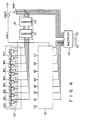
- F ig. 6 shows an apparatus which can divide the elements of the Galois field GF(2 8 ) in the manner described above.
- the apparatus comprises a converter 51.
- the converter 51 includes a decoder 511 and an encoder 512, both being ROMs storing data representing the reciprocal ⁇ 255-x which is supplied from the converter 51 when the converter 51 receives data representing an element of each of n groups which is located at the first location, i.e., element a X .
- n 32 and the first element of each group is denoted by a l .
- the converter 51 stores a table of reciprocal conversions concerning elements ⁇ 8k+1 , where k . 0, 1, 2, ... 31. The table is as shown below:
- the converter 51 When any address shown in the table is designated, the converter 51 outputs reciprocal data representing the reciprocal of the element a 8k+l corresponding to the address. When any address other than those shown in the table is designated, the converter 51 outputs no reciprocal data.
- the apparatus shown in Fig. 6 further comprises two linear shift registers 52 and 53, both being identical to the linear shift register SR O shown in Fig. 5.
- Data representing dividend a i and data representing divider ⁇ j are stored in these shift registers 52 and 53, respectively.
- the dividend a i and divider ⁇ j are expressed as follows:
- the output data from the shift register 52 are supplied to the multiplier input terminals of a multiplier 54.
- the output data from the shift register 53 are supplied to the input terminals of the decoder 5ll of the converter 51.
- the output data from the encoder 512 of the converter 51 are supplied to the multiplicand input terminals of the multiplier 54 and also to the input terminals of a NOR gate NOR 1 .
- the output from the NOR gate NOR 1 is supplied to one input terminal of an AND gate AND 10 , the other input terminal of which is connected to the clock pulse generator (not shown).
- the output from the NOR gate NOR l is used to generate a control clock signal SOK-1 for controlling the shift registers 52 and 53.
- the multiplier 54 has the same structure as the multiplier illustrated in Fig. 5.
- the apparatus shown in Fi g. 6 performs the division ai ⁇ j in the following manner. If the data stored in the shift register 53 and representing the divider ⁇ j are found in the conversion table which is stored in the converter 51, the reciprocal data ⁇ -j from the converter 51 is supplied as multiplier data to the multiplier 54. The data stored in the shift register 52 and representing the dividend a i , or multiplicand a i are supplied to the multiplier 54. The multiplier 54 multiplies the multiplicand a i by the multiplier ⁇ -j .
- the divider aj is repeatedly multiplied by a (N times; 0 ⁇ N ⁇ 7) until aj +N becomes equal to one of the elements ⁇ 8k+1 of the conversion table. In this way, a reciprocal data ⁇ -(j+N) is obtained.
- the dividend a i is also multiplied by a N , thus providing data representing a i+N .
- the result of the multiplication performed by the multiplier 54 is thus:
- Component a- N can therefore be removed. Any element a i of the Galois field GF(2 8 ) can thus be divided by any other element of the Galois field even if a conversion table of all elements a l to a 25 5 is not stored in the converter 51.
- control clock signals SCK-1 are supplied from the AND gate AND 10 which produces a logical product of the output from the NOR gate NOR 1 and a clock pulse CP, as long as the NOR gate NOR 1 keeps generating outputs of logical "1" level.
- the AND gate AND 10 continues to generate control clocks SCK-1 until the converter 51 receives divider data ⁇ j which is identical to data a 8k+l . Every time the shift register 52 receives a control clock SCK-1, ⁇ i is multiplied by a. Similarly, every time the shift register 53 receives a control clock signal, SCK-1, ⁇ j is multiplied by a.
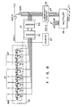
- Fig. 8 illustrates another apparatus of the present invention for dividing the elements of the Galois field GF(2 8 ).
- the apparatus comprises a linear shift register 53 which is designed to receive data representing divider ⁇ j and to supply the data to a decoder 511 provided in a converter 51.
- An encoder 512 is provided in the converter 51 and connected to the output of the decoder 511.
- Output data from the encoder 512 are supplied to a linear shift register 56 and also to the input terminals of a NOR gate NOR 1 .
- the output from the NOR gate NOR 1 is supplied to an AND gate AND 10 .
- the AND gate AND 10 generates a control clock SCK-1 when it receives the output from the NOR gate NOR 1 and a clock pulse CP.
- the control clock signal SCK-1 i.e., the logical product of the output from the NOR gate NOR 1 and the clock pulse CP, is supplied to the shift register 53 and controls the same.
- the control clock signal SCK-1 is supplied to a counter 57 and is then used as a control clock signal SCK-2 for controlling the shift register 56.
- the apparatus shown in Fig. 8 further comprises a multiplier 55.
- the multiplier 55 receives data representing dividend a i . It also receives data representing the divider ⁇ j supplied from the shift register 56.
- the dividend a i and the divider ⁇ j are given as follows:
- the shift register 53 is identical with the linear shift register SR O shown in Fig. 5.
- the multiplier 55 is identical with the multiplier 54 shown in Fig. 6.
- the data stored in the shift register 53 and representing the divider ⁇ j are found in a conversion table which is stored in the converter 51, the data representing the reciprocal ⁇ -j of the divider ⁇ j are supplied from the converter 51 as multiplier data to the multiplier 55 through the shift register 56.
- the multiplier 55 multiplies the dividend ⁇ i supplied to it by the reciprocal ⁇ -j .
- the multiplier 55 performs the multiplication: ⁇ i ⁇ a -j .
- the divider aj is repeatedly multiplied by (N times; 0 ⁇ N ⁇ 7) until aj +N becomes equal to one of the elements a 8k+l of the conversion table. In this way, the reciprocal data ⁇ -(j+N) is obtained. If the reciprocal data ⁇ -(j+N) , i.e., ⁇ -j ⁇ -N , is multiplied by a N , then:
- the divider a3 is repeatedly multiplied by a as the linear shift register 53 is shifted N times so that the converter 51 generates reciprocal data ⁇ -(j+N) .
- the reciprocal ⁇ -(j+N) is multiplied by a N as the linear shift register 56 is shifted N times, so that the shift register 56 generates desired reciprocal data ⁇ -j .
- the shift register 53 is automatically shifted N times. This is because control clock signals SCK-l are supplied to the shift register 53 from the AND gate AND 10 which produces a logical product of the output from the NOR gate NOR 1 and a clock pulse CP, as long as the NOR gate NOR 1 keeps generating outputs of logical "1" level. In other words, the AND gate AND 10 continues to generate control clock signals SCK-1 until the converter 51 receives divider data ⁇ j which is identical with data a 8k+l . Every time the shift register 52 receives a control clock SCK-1, a i is multiplied by a.
- the shift register 56 which stores the reciprocal data ⁇ -(j+N) is automatically shifted N times, too. This is because the counter 57 counts the control clock signals SCK-1 from the AND gate AND 10 and supplies them as control clock signals SCK-2 to the linear shift register 56.
- the number of control clock signals SCK-2 supplied to the shift register 56 is of course the same as that of control clock signals SCK-1 supplied to the shift register 53. Every time the shift register 56 receives a control clock signal SCK-2, the reciprocal data a-( J+N ) is multiplied by a N .
- the data representing element a i and the data representing element ⁇ -j are supplied to the multiplier 55. And the multiplier 55 multiplies element a i by element a-j, thus performing the division: ⁇ i ⁇ ⁇ j .
- the data representing ⁇ 142 are supplied to the shift register 56.
- the shift register 56 is shifted three times, thus changing the input data to ⁇ 145 which is the reciprocal of the divider ⁇ 110 .
- Data representing ⁇ 110 are supplied to the multiplier 55.
- Data representing the dividend ⁇ 80 are also supplied to the multiplier 55.
- the multiplier 55 multiplies the dividend a 80 by the reciprocal a 145 of the divider a ll0. That is:
- one of the elements of the Galois field GF(2 m ) is divided by another element of the Galois field GF(2 m ) by multiplying the first element by the reciprocal of the second element.
- the division can therefore be achieved without using a logarithm buffer or an antilogarithm buffer, that is, without a ROM having a great memory capacity storing either a logarithm table or an antilogarithm table.
- a memory of a relatively small memory capacity suffices to store data necessary for obtaining data representing the reciprocal of each divider.
- the apparatus of the invention may be used in combination with a system for recording, reproducing and transmitting digital data such as PCM data, a system for processing such data or any other system in which one of the elements of the Galois field needs to be divided by another element of the Galois field.
- the present invention can provide an apparatus for dividing the elements of a Galois field, which has neither a logarithm buffer nor an antilogarithm buffer, both of which require a large memory capacity, and which therefore has a simple structure and can be manufactured at low cost.
Applications Claiming Priority (4)
| Application Number | Priority Date | Filing Date | Title |
|---|---|---|---|
| JP102807/82 | 1982-06-15 | ||
| JP57102804A JPS58219648A (ja) | 1982-06-15 | 1982-06-15 | ガロア体における除算装置 |
| JP102804/82 | 1982-06-15 | ||
| JP57102807A JPS58219650A (ja) | 1982-06-15 | 1982-06-15 | ガロア体における除算装置 |
Publications (3)
| Publication Number | Publication Date |
|---|---|
| EP0096165A2 true EP0096165A2 (fr) | 1983-12-21 |
| EP0096165A3 EP0096165A3 (en) | 1984-10-17 |
| EP0096165B1 EP0096165B1 (fr) | 1988-06-08 |
Family
ID=26443483
Family Applications (1)
| Application Number | Title | Priority Date | Filing Date |
|---|---|---|---|
| EP83102308A Expired EP0096165B1 (fr) | 1982-06-15 | 1983-03-09 | Appareil pour diviser les éléments d'un champ de Galois |
Country Status (4)
| Country | Link |
|---|---|
| US (1) | US4567568A (fr) |
| EP (1) | EP0096165B1 (fr) |
| KR (1) | KR860001341B1 (fr) |
| DE (1) | DE3377029D1 (fr) |
Cited By (7)
| Publication number | Priority date | Publication date | Assignee | Title |
|---|---|---|---|---|
| GB2149540A (en) * | 1983-11-10 | 1985-06-12 | Gen Signal Corp | Vital processor |
| EP0152702A2 (fr) * | 1983-12-30 | 1985-08-28 | Sony Corporation | Circuit arithmétique d'un champ fini |
| EP0169908A1 (fr) * | 1984-01-21 | 1986-02-05 | Sony Corporation | Procédé et circuit de décodage de données de code d'erreurs |
| EP0447245A2 (fr) * | 1990-03-14 | 1991-09-18 | International Business Machines Corporation | Procédé et appareil de division en mode sérielle par bit |
| GB2253975A (en) * | 1991-03-20 | 1992-09-23 | Samsung Electronics Co Ltd | Processing images, sound or data encoded in error correcting code using Galois Field arithmetic |
| EP0566215A3 (en) * | 1986-09-30 | 1994-05-18 | Canon Kk | Error correction apparatus |
| WO1996008875A1 (fr) * | 1994-09-16 | 1996-03-21 | Cirrus Logic, Inc. | Circuit de calcul de correction d'erreurs a usages multiples |
Families Citing this family (23)
| Publication number | Priority date | Publication date | Assignee | Title |
|---|---|---|---|---|
| US4975867A (en) * | 1987-06-26 | 1990-12-04 | Digital Equipment Corporation | Apparatus for dividing elements of a Galois Field GF (2QM) |
| AU613701B2 (en) * | 1987-06-26 | 1991-08-08 | Digital Equipment Corporation | Apparatus for computing multiplicative inverses in data encoding decoding devices |
| EP0466814A4 (en) * | 1989-04-10 | 1993-02-24 | Motorola Inc. | Integer divider circuit |
| US5020017A (en) * | 1989-04-10 | 1991-05-28 | Motorola, Inc. | Method and apparatus for obtaining the quotient of two numbers within one clock cycle |
| US5185711A (en) * | 1989-12-08 | 1993-02-09 | Sony Corporation | Apparatus for dividing elements of a finite galois field and decoding error correction codes |
| IL94449A (en) * | 1990-05-20 | 1994-06-24 | Fortress U & T 2000 Ltd | Method and apparatus for exponentiation over gf(2") |
| US5245564A (en) * | 1991-05-10 | 1993-09-14 | Weitek Corporation | Apparatus for multiplying operands |
| JP3232602B2 (ja) * | 1991-09-06 | 2001-11-26 | ソニー株式会社 | ユークリッドの互除回路 |
| US5379243A (en) * | 1992-08-31 | 1995-01-03 | Comstream Corporation | Method and apparatus for performing finite field division |
| WO1995012845A1 (fr) * | 1993-11-04 | 1995-05-11 | Cirrus Logic, Inc. | Inversion de corps de galois |
| US5493522A (en) * | 1994-09-21 | 1996-02-20 | Northrop Grumman Corporation | Fast arithmetic modulo divider |
| US6098192A (en) * | 1997-09-17 | 2000-08-01 | Cirrus Logic, Inc. | Cost reduced finite field processor for error correction in computer storage devices |
| JPH1196030A (ja) * | 1997-09-22 | 1999-04-09 | Toyo Commun Equip Co Ltd | 有限体上の乗算方法及び乗算回路 |
| US6286022B1 (en) | 1997-11-18 | 2001-09-04 | Rsa Security Inc. | Efficient finite field basis conversion involving a dual basis |
| US6377969B1 (en) * | 1999-04-23 | 2002-04-23 | General Dynamics Government Systems Corporation | Method for multiplication in Galois fields using programmable circuits |
| US6584483B1 (en) * | 1999-12-30 | 2003-06-24 | Intel Corporation | System and method for efficient hardware implementation of a perfect precision blending function |
| US7178091B1 (en) | 2001-07-10 | 2007-02-13 | National Semiconductor Corporation | Reed solomon encoder |
| US7403964B2 (en) * | 2002-10-22 | 2008-07-22 | Broadcom Corporation | Galois field multiplier array for use within a finite field arithmetic unit |
| US20070127431A1 (en) * | 2005-11-11 | 2007-06-07 | Samsung Electronics Co., Ltd. | Method and apparatus for generating pseudorandom binary sequence in communication system using linear feedback shift register |
| JP4891704B2 (ja) * | 2006-08-28 | 2012-03-07 | 株式会社東芝 | 半導体記憶装置 |
| US8176395B2 (en) * | 2007-11-27 | 2012-05-08 | Macronix International Co., Ltd. | Memory module and writing and reading method thereof |
| JP5259343B2 (ja) * | 2008-10-31 | 2013-08-07 | 株式会社東芝 | メモリ装置 |
| JP5422974B2 (ja) * | 2008-11-18 | 2014-02-19 | 富士通株式会社 | 誤り判定回路及び共有メモリシステム |
Citations (5)
| Publication number | Priority date | Publication date | Assignee | Title |
|---|---|---|---|---|
| US3533067A (en) * | 1967-06-15 | 1970-10-06 | Mitre Corp | Error correcting digital coding and decoding apparatus |
| US3648236A (en) * | 1970-04-20 | 1972-03-07 | Bell Telephone Labor Inc | Decoding method and apparatus for bose-chaudhuri-hocquenghem codes |
| US4162480A (en) * | 1977-01-28 | 1979-07-24 | Cyclotomics, Inc. | Galois field computer |
| GB2050014A (en) * | 1979-05-10 | 1980-12-31 | Tokyo Shibaura Electric Co | Error date correcting system |
| GB2079994A (en) * | 1980-06-20 | 1982-01-27 | Sony Corp | Methods of digital data error correction |
Family Cites Families (3)
| Publication number | Priority date | Publication date | Assignee | Title |
|---|---|---|---|---|
| US3633018A (en) * | 1969-12-18 | 1972-01-04 | Ibm | Digital division by reciprocal conversion technique |
| US4142174A (en) * | 1977-08-15 | 1979-02-27 | International Business Machines Corporation | High speed decoding of Reed-Solomon codes |
| JPS57155667A (en) * | 1981-03-23 | 1982-09-25 | Sony Corp | Arithmetic circuit of galois matter |
-
1983
- 1983-03-09 EP EP83102308A patent/EP0096165B1/fr not_active Expired
- 1983-03-09 DE DE8383102308T patent/DE3377029D1/de not_active Expired
- 1983-03-10 US US06/473,767 patent/US4567568A/en not_active Expired - Lifetime
- 1983-05-11 KR KR8302027A patent/KR860001341B1/ko not_active IP Right Cessation
Patent Citations (5)
| Publication number | Priority date | Publication date | Assignee | Title |
|---|---|---|---|---|
| US3533067A (en) * | 1967-06-15 | 1970-10-06 | Mitre Corp | Error correcting digital coding and decoding apparatus |
| US3648236A (en) * | 1970-04-20 | 1972-03-07 | Bell Telephone Labor Inc | Decoding method and apparatus for bose-chaudhuri-hocquenghem codes |
| US4162480A (en) * | 1977-01-28 | 1979-07-24 | Cyclotomics, Inc. | Galois field computer |
| GB2050014A (en) * | 1979-05-10 | 1980-12-31 | Tokyo Shibaura Electric Co | Error date correcting system |
| GB2079994A (en) * | 1980-06-20 | 1982-01-27 | Sony Corp | Methods of digital data error correction |
Non-Patent Citations (4)
| Title |
|---|
| IEEE TRANSACTIONS ON COMMUNICATIONS, vol. COM-24, no. 4, April 1976, pages 438-440, New York, USA; PO HSIIN CHEN: "Multisequence linear shift register synthesis and its application to BCH decoding" * |
| IEEE TRANSACTIONS ON INFORMATION THEORY, vol. IT-22, no. 2, March 1976, pages 237-238, New York, US A; J. JUSTESEN: "On the complexity of decoding Reed-Solomon codes" * |
| PETERSON: Error Correcting Codes ( MIT Press 1972) pp. 178-180 * |
| PROCEEDINGS OF THE SYMPOSIUM ON COMPUTER PROCESSING IN COMMUNICATIONS, New York, 8th-10th April 1969, pages 401-413, Polytechnik Press, Brooklyn, USA; A.M. MICHELSON: "Computer implementation of decoders for several BCH codes" * |
Cited By (15)
| Publication number | Priority date | Publication date | Assignee | Title |
|---|---|---|---|---|
| GB2149540A (en) * | 1983-11-10 | 1985-06-12 | Gen Signal Corp | Vital processor |
| GB2169114A (en) * | 1983-11-10 | 1986-07-02 | Gen Signal Corp | Vital processor v |
| EP0152702A3 (en) * | 1983-12-30 | 1986-10-01 | Sony Corporation | Arithmetic circuit of finite field |
| EP0152702A2 (fr) * | 1983-12-30 | 1985-08-28 | Sony Corporation | Circuit arithmétique d'un champ fini |
| US4800515A (en) * | 1984-01-21 | 1989-01-24 | Sony Corporation | Circuit for operating finite fields |
| EP0169908A4 (fr) * | 1984-01-21 | 1988-05-10 | Sony Corp | Procédé et circuit de décodage de données de code d'erreurs. |
| EP0169908A1 (fr) * | 1984-01-21 | 1986-02-05 | Sony Corporation | Procédé et circuit de décodage de données de code d'erreurs |
| EP0566215A3 (en) * | 1986-09-30 | 1994-05-18 | Canon Kk | Error correction apparatus |
| US5590138A (en) * | 1986-09-30 | 1996-12-31 | Canon Kabushiki Kaisha | Error correction apparatus |
| US5774389A (en) * | 1986-09-30 | 1998-06-30 | Canon Kabushiki Kaisha | Error correction apparatus |
| EP0447245A2 (fr) * | 1990-03-14 | 1991-09-18 | International Business Machines Corporation | Procédé et appareil de division en mode sérielle par bit |
| EP0447245A3 (en) * | 1990-03-14 | 1993-02-03 | International Business Machines Corporation | Bit-serial division method and apparatus |
| GB2253975A (en) * | 1991-03-20 | 1992-09-23 | Samsung Electronics Co Ltd | Processing images, sound or data encoded in error correcting code using Galois Field arithmetic |
| GB2253975B (en) * | 1991-03-20 | 1994-05-25 | Samsung Electronics Co Ltd | An apparatus operating on a galois field over gf (2m) |
| WO1996008875A1 (fr) * | 1994-09-16 | 1996-03-21 | Cirrus Logic, Inc. | Circuit de calcul de correction d'erreurs a usages multiples |
Also Published As
| Publication number | Publication date |
|---|---|
| EP0096165B1 (fr) | 1988-06-08 |
| KR860001341B1 (en) | 1986-09-15 |
| DE3377029D1 (en) | 1988-07-14 |
| US4567568A (en) | 1986-01-28 |
| EP0096165A3 (en) | 1984-10-17 |
Similar Documents
| Publication | Publication Date | Title |
|---|---|---|
| EP0096165B1 (fr) | Appareil pour diviser les éléments d'un champ de Galois | |
| EP0096163B1 (fr) | Appareil pour diviser les éléments d'un champ de Galois | |
| EP0096109B1 (fr) | Système de correction d'erreurs | |
| US4763332A (en) | Shared circuitry for the encoding and syndrome generation functions of a Reed-Solomon code | |
| EP0329789B1 (fr) | Unite arithmetique a champ de galois | |
| EP0096164A2 (fr) | Circuit de modulation par durée d'impulsions | |
| EP0136587B1 (fr) | Circuit de correction d'erreur | |
| US5490154A (en) | Method of and circuit arrangement for decoding RS-coded data signals | |
| JPH0553087B2 (fr) | ||
| EP0169908B1 (fr) | Procédé et circuit de décodage de données de code d'erreurs | |
| US5541940A (en) | Error correction method and error correction circuit | |
| EP1442528A2 (fr) | Procede de decodage et decodeur pour code reed solomon | |
| JPS638648B2 (fr) | ||
| WO1999016175A1 (fr) | Circuit integre a semi-conducteurs et systeme de traitement de donnees | |
| JP3281938B2 (ja) | 誤り訂正装置 | |
| JPS6237415B2 (fr) | ||
| JPS638650B2 (fr) | ||
| JPS6248254B2 (fr) | ||
| JPS638649B2 (fr) | ||
| JPH09305572A (ja) | ガロア体の除算方法および除算装置 | |
| JPS6246018B2 (fr) | ||
| JPS6237414B2 (fr) | ||
| JPH0834439B2 (ja) | ガロア体演算装置 | |
| JPS63131623A (ja) | チエンのアルゴリズム実現装置 | |
| JP2002207593A (ja) | ガロア体乗算器およびガロア体除算器 |
Legal Events
| Date | Code | Title | Description |
|---|---|---|---|
| PUAI | Public reference made under article 153(3) epc to a published international application that has entered the european phase |
Free format text: ORIGINAL CODE: 0009012 |
|
| 17P | Request for examination filed |
Effective date: 19830309 |
|
| AK | Designated contracting states |
Designated state(s): DE FR GB NL |
|
| PUAL | Search report despatched |
Free format text: ORIGINAL CODE: 0009013 |
|
| RAP1 | Party data changed (applicant data changed or rights of an application transferred) |
Owner name: KABUSHIKI KAISHA TOSHIBA |
|
| AK | Designated contracting states |
Designated state(s): DE FR GB NL |
|
| 17Q | First examination report despatched |
Effective date: 19860516 |
|
| GRAA | (expected) grant |
Free format text: ORIGINAL CODE: 0009210 |
|
| AK | Designated contracting states |
Kind code of ref document: B1 Designated state(s): DE FR GB |
|
| REF | Corresponds to: |
Ref document number: 3377029 Country of ref document: DE Date of ref document: 19880714 |
|
| ET | Fr: translation filed | ||
| PLBE | No opposition filed within time limit |
Free format text: ORIGINAL CODE: 0009261 |
|
| STAA | Information on the status of an ep patent application or granted ep patent |
Free format text: STATUS: NO OPPOSITION FILED WITHIN TIME LIMIT |
|
| 26N | No opposition filed | ||
| REG | Reference to a national code |
Ref country code: GB Ref legal event code: IF02 |
|
| PGFP | Annual fee paid to national office [announced via postgrant information from national office to epo] |
Ref country code: FR Payment date: 20020312 Year of fee payment: 20 |
|
| PGFP | Annual fee paid to national office [announced via postgrant information from national office to epo] |
Ref country code: GB Payment date: 20020313 Year of fee payment: 20 |
|
| PGFP | Annual fee paid to national office [announced via postgrant information from national office to epo] |
Ref country code: DE Payment date: 20020327 Year of fee payment: 20 |
|
| PG25 | Lapsed in a contracting state [announced via postgrant information from national office to epo] |
Ref country code: GB Free format text: LAPSE BECAUSE OF EXPIRATION OF PROTECTION Effective date: 20030308 |
|
| REG | Reference to a national code |
Ref country code: GB Ref legal event code: PE20 |