EP0091695A2 - Circuit économiseur de batterie pour un récepteur d'appel - Google Patents
Circuit économiseur de batterie pour un récepteur d'appel Download PDFInfo
- Publication number
- EP0091695A2 EP0091695A2 EP83103568A EP83103568A EP0091695A2 EP 0091695 A2 EP0091695 A2 EP 0091695A2 EP 83103568 A EP83103568 A EP 83103568A EP 83103568 A EP83103568 A EP 83103568A EP 0091695 A2 EP0091695 A2 EP 0091695A2
- Authority
- EP
- European Patent Office
- Prior art keywords
- output
- flip
- flop
- battery saver
- circuit
- Prior art date
- Legal status (The legal status is an assumption and is not a legal conclusion. Google has not performed a legal analysis and makes no representation as to the accuracy of the status listed.)
- Granted
Links
- 238000007493 shaping process Methods 0.000 claims description 8
- 230000007704 transition Effects 0.000 claims description 8
- 238000001514 detection method Methods 0.000 claims description 6
- 230000004044 response Effects 0.000 claims description 6
- 230000000737 periodic effect Effects 0.000 abstract description 5
- 230000005540 biological transmission Effects 0.000 description 7
- 238000010586 diagram Methods 0.000 description 4
- 230000008054 signal transmission Effects 0.000 description 3
- 230000000630 rising effect Effects 0.000 description 2
- 238000000034 method Methods 0.000 description 1
- 238000012986 modification Methods 0.000 description 1
- 230000004048 modification Effects 0.000 description 1
- 238000009877 rendering Methods 0.000 description 1
- 230000003252 repetitive effect Effects 0.000 description 1
- 230000001960 triggered effect Effects 0.000 description 1
Images


Classifications
-
- H—ELECTRICITY
- H04—ELECTRIC COMMUNICATION TECHNIQUE
- H04B—TRANSMISSION
- H04B5/00—Near-field transmission systems, e.g. inductive loop type
-
- H—ELECTRICITY
- H04—ELECTRIC COMMUNICATION TECHNIQUE
- H04W—WIRELESS COMMUNICATION NETWORKS
- H04W52/00—Power management, e.g. TPC [Transmission Power Control], power saving or power classes
- H04W52/02—Power saving arrangements
- H04W52/0209—Power saving arrangements in terminal devices
- H04W52/0225—Power saving arrangements in terminal devices using monitoring of external events, e.g. the presence of a signal
- H04W52/0229—Power saving arrangements in terminal devices using monitoring of external events, e.g. the presence of a signal where the received signal is a wanted signal
-
- G—PHYSICS
- G08—SIGNALLING
- G08B—SIGNALLING OR CALLING SYSTEMS; ORDER TELEGRAPHS; ALARM SYSTEMS
- G08B3/00—Audible signalling systems; Audible personal calling systems
- G08B3/10—Audible signalling systems; Audible personal calling systems using electric transmission; using electromagnetic transmission
- G08B3/1008—Personal calling arrangements or devices, i.e. paging systems
- G08B3/1016—Personal calling arrangements or devices, i.e. paging systems using wireless transmission
- G08B3/1025—Paging receivers with audible signalling details
- G08B3/1066—Paging receivers with audible signalling details with other provisions not elsewhere provided for, e.g. turn-off protection
-
- H—ELECTRICITY
- H04—ELECTRIC COMMUNICATION TECHNIQUE
- H04W—WIRELESS COMMUNICATION NETWORKS
- H04W88/00—Devices specially adapted for wireless communication networks, e.g. terminals, base stations or access point devices
- H04W88/02—Terminal devices
- H04W88/022—Selective call receivers
-
- Y—GENERAL TAGGING OF NEW TECHNOLOGICAL DEVELOPMENTS; GENERAL TAGGING OF CROSS-SECTIONAL TECHNOLOGIES SPANNING OVER SEVERAL SECTIONS OF THE IPC; TECHNICAL SUBJECTS COVERED BY FORMER USPC CROSS-REFERENCE ART COLLECTIONS [XRACs] AND DIGESTS
- Y02—TECHNOLOGIES OR APPLICATIONS FOR MITIGATION OR ADAPTATION AGAINST CLIMATE CHANGE
- Y02D—CLIMATE CHANGE MITIGATION TECHNOLOGIES IN INFORMATION AND COMMUNICATION TECHNOLOGIES [ICT], I.E. INFORMATION AND COMMUNICATION TECHNOLOGIES AIMING AT THE REDUCTION OF THEIR OWN ENERGY USE
- Y02D30/00—Reducing energy consumption in communication networks
- Y02D30/70—Reducing energy consumption in communication networks in wireless communication networks
Definitions
- This invention relates generally to a battery saver circuit for use with a paging receiver, which saver circuit is provided for periodically supplying power to the receiver in short time duration instead of continuously and for keeping the receiver on in the event that the presence of code signals is detected which signals are transmitted subsequently after a preamble.
- Radio paging systems have proven very popular and many efforts have been made to reduce the size, weight, and power consumption of same through the use of integrated circuits.
- battery saving circuits are used to minimize power consumption by periodically supplying power to a receiver in short bursts instead of continuously.
- Presently known battery saver circuits operating in radio pager receiver periodically supply power, enabling the search for the presence of a preamble code which if found, extend the time period for which power is supplied to permit further search for predetermined sequential codes.
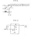
- Fig. 1A shows a code sequence transmitted from a calling station, wherein a preamble P with a time period T is followed by message and end codes (A and E respectively).
- Fig. 1B shows pulses B' each having a time period Tl which represents the time duration for which power is supplied to high power drain circuits of the receiver. During this time period Tl, the pager receiver is rendered operative and is permitted to search for the preamble.
- the time periods Tl, T2 power on and off periods respectively
- occur sequentially and are chosen to satisfy the equation (2T1 + T2 T) so that each of the repetitive pulses B must occur within the duration of a preamble.
- Fig. lC shows the application of power to the pager receiver as a result of the detection of the preamble.
- Fig.2 shows a standard code format proposed by the POCSAG (British Post Office Code Standardisation Advisory Group).
- a transmission consists of a preamble P followed by batches 1, 2, 3, ..., each batch beginning with a synchronization codeword (SC). The transmission ceases when there are no further calls.
- SC synchronization codeword
- Each transmission starts with a preamble to permit the pagers to attain bit synchronization and to prepare them to acquire word synchronization.
- the preamble is a pattern of reversals, 101010..., repeated for a period of at least 576 bits, i.e., the duration of a batch plus a codeword.
- Codewords are transmitted in batches each of which comprises an SC followed by 8 groups or frames each containing 2 codewords.
- the detailed explanation of the above, is given in the document entitled "A Standard Code for Radiopaging" (available from: Telecommunications Development Department, TD4.2.3. 2-12 Gresham Street, London EC2V7AG, United Kingdom).
- the preamble is added to the head of a new sequence of calling signals whereby if continuous callings occur then another preamble is not transmitted until the interruption of the callings and the occurrence of the next new signal transmission.
- the foregoing power consumption technique in which power is supplied periodically, is applied to the pager receiver operable on the POCSAG code signals, a subcriber may miss the reception of his caller's message. More specifically, if a subscriber switches on to energize his pager after the preamble has already been transmitted, he can no longer receive any message signals.
- a similar problem may also be encountered when a subscriber is within a building, in the subway or the like where paging signals are too weak to be receive and the preamble goes undetected.
- the present invention features a battery saver circuit which both conserves battery energy and allows for the prolonging of the energization of high power drain circuits in the event that a valid incoming signal is received during any periodic brief (battery saving) circuit energization, whereby the inclusion of a specific address code may be ascertained and the subscriber is alerted.
- the present invention takes the form of a battery saver circuit for use with a pager receiver including, a front end having a demodulator for demodulating an incoming signal, a wave shaping circuit coupled to said front end for producing a rectangular signal responsive to the output of said front end, and a battery saver control for periodically supplying power to the receiver under control of timing pulses, said battery saver circuit, comprising: a valid incoming signal detector adapted to receive the output of the wave shaping circuit for detecting the frequency or bits per second of the incoming signal and producing a first logic signal indicative of the detection of a valid incoming signal;-and a battery saver terminating means responsive to said first logic signal to generate a second logic signal for extending the time period for which power is supplied to the receiver.
- Fig. 3 there is shown an arrangement in which a DC power source 8 is coupled through an apparatus switch 9 to a decoder 4, an electric switch 10 and a loudspeaker driver 6.
- the decoder 4 which is directly concerned with this invention will be discussed in detail subsequently.
- Each circuit section to which the D C power source 8 is directly coupled consumes relatively little power.
- the decoder 4 periodically supplies a control signal B to the switch 10 to periodically turn same and avoid continious power consumption. However, upon the detection of a batch or message transmission, the decoder 4 maintains the switch 10 on to enable the search for a predetermined sequential code.
- Switch 10 applies power to a front end 2 (a high frequency receiver section) and a wave shaper 3 when turned on.
- Front end 2 is provided for amplifying and demodulating the code-modulated carrier wave received by antenna 1.
- Front end 2 is a conventional circuit arrangement comprised of a high frequency amplifier, a frequency converter, an IF amplifier, and a discriminator.
- the output of front end 2 is applied to a wave-shaper 3 which generates an output signal S consisting of a series of rectangular pulses.
- the signal S from wave-shaper 3 is supplied to the decoder 4 which is also coupled to PROM (Programable Read Only Memory) 5.
- Decoder 4 searches for an identifying address code by comparing same with a subcriber's unique code prestored in PROM 5. Upon the detection of the identifying address code, a . signal A is fed to driver 6 to activate a loudspeaker 7 for alerting a subscriber.
- the battery saver circuit of this invention forming part of the decoder 4, will now be described in detail with reference to Figs. 5 and 6, wherein assuming that a preamble has already transmitted and subsequent massege or batch codes are receivable.
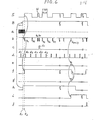
- FIG. 5 When the circuit of Fig. 5 is initially rendered operative by turning on the main switch 9 (Fig.3), all the D flip-flops of the circuit are reset.
- a battery saver control circuit 52 periodically outputs pulses "h" at a prefixed interval although only one is shown in Fig. 6. The occurrence of the control pulse "h” is controlled by timing pulses "a" applied from a clock generator 47 of a multi-timer 50.
- the pulse “h” passes' through an OR gate 53 and is then applied, via an output terminal 54, to the switch 10 (Fig. 3) as control signal B.
- the signal B actuates the switch 10 for periodically supplying power to the front end 2 and the wave-shaping circuit 3 (Fig. 3).
- a pulse "i” assumes a low logic state.
- the periodic power supply is terminated allowing the receiver to search for an identifying address code involved in batch or message codes. The transition of pulse "i" from low level to the high will be decribed later on.
- the multi-timer 50 comprises the clock 47 and two D flip-flops 48, 49.
- the flip-flops 48 and 49 have been initially reset as referred to previously.
- the flip-flop 48 changes its logic state every two occurrences of timing pulses "a” and thus the output Q of flip-flop 49 assumes a low logic state every four timining pulses "a".
- a timer 28 responds to the high logic signal applied from the flip-flop 49 generating a train of pulses "d" (d l , d 2 , d 3 , d 4 ,.7) each of which has a time duration identical with that of one bit of a desired incoming signal.
- the pulse "d” is inverted by an inverter 33 and then the inverted pulse sets the flip-flops 16 and 17 through an NAND gate 55, and is also directly applied to and resets a D flip-flop 27.
- the pulse B goes high in response thereto.
- the flip-flop 16 is reset and creates a low logic state at its output Q while the flip-flop 17 remains set in that the signal S is inverted by an inverter 18.
- a NAND gate 19 creates a high logic state in response to the resetting of the flip-flop 16, and thus sets a D flip-flop 22 of a shift register 25 in response to the rising edge of the pulse created on the Q output of the flip-flop 48.
- the differentiator 20 includes the two flip-flops 16 and 17, the inverter 18 and the NAND gate 19.
- a D flip-flop 42 of a battery saver inhibit circuit 45 remains reset so that the output pulse "b" of a NAND gate 24 remains high prior to the setting of flip-flop 22.
- the output of AND gate 24 is switched to the low level (a pulse "b 1 ").
- the setting of flip-flop 22 also allows a D flip-flop 23 to RS flip-flop consisting of two NAND gates 31 and 32, the NAND gate 33, the timer 28 and an inverter 33', all of which are coupled as shown.
- the timer 28 outputs a train of reset pulses d l , d 2 , d 3 , d 4 , ....'each having a period identical with the time duration of one bit of a valid incoming signal.
- the signal "d" is used to periodically reset the flip-flop 27 which therefore periodically creates a low logic state on its output Q resulting in a high logic state on the output of NAND gate 30.
- a counter 36 be set in response to the rising edge of the pulse created on Q output of flip-flop 49 and thus creates a low logic state on its Q output. Therefore the flip-flop 16 is again set by a high logic output of the NAND gate 55 irrespective of the output of the NAND gate 33. Now that both flip-flops 16 and 17 have been set, the NAND gate 19 subsesquently exhibits a low logic state with the result of a high logic state present on the Q output of the flip-flop 22, thereby resulting in a high logic state of the signal "b 1 ".
- the shift register 25 includes the two flip-flops 22, 23, and the NAND gate 24.
- the flip-flop 17 responds to the transition of signal S from a high logic level to the low through the provision of inverter 18, in the case of which it should be noted that the flip-flop 16 in turn remains set.
- a noise detector 34 will hereinafter be discussed which comprises the aforementioned flip-flop 27, a RS flip-flop consisting of two NAND gates 29 and 30, another counts the pulse b l , and a timer 37 is triggered by the trailing edge of pulse b 1 to generate a pulse "f" having a high logic level with a predetermined time duration.
- the counter 36 and the timer 37 define a valid incoming signal detector 40, together with an OR gate 38 and an AND gate 39.
- the pulse b 1 sets the flip-flop 27 resulting in a high logic state present on the Q output thereof. However, the flip-flop 27 is again reset by the subsequently occurring pulses d 2 and d 3 .
- pulse b 2 following b 1 is also counted by the counter 36 and sets the flip-flop 27 which will again be reset by pulse d4. If noise N occurs between pulses d 4 and d 5 , then pulses b 3 and b 4 are generated accordingly and creates a pulse c 1 on the output of inverter 33'. Thus pulse c 1 resets or zeros out the counter 36 which is set by pulse b 5 again commencing the counting of the pulses "b".
- the counter 36 counts up a prefixed number of pulses "b” by counting a pulse b (m+1)' it produces a pulse "e”.
- a pulse “g” is created from the AND gate 39, which pulse “g” indicates that a valid incoming signal followed by the preamble is detected.
- the pulse “g” is applied to the clock terminal C of the flip-flop 42 thereby setting same.
- the pulse “g” is further used to reset both the counter 36 and the timer 37.
- the setting of the flip-flop 42 results in a high logic state on its Q output (pulse "i") and also results in a low logic state on its Q output thereby closing the NAND gate 24 of the shift register 25.
- the pulse "i” is fed to an AND gate 44 which responds to the timing pulse "a” applying a trigger pulse for rendering a timer 43 operative.
- timer 43 generates a pulse "j" after a time period selected so that the pager receiver can detect the message codes.
- the pulse "j" resets flip-flop 42, timer 43, and battery saver control circuit 52.
- Fig. 7 is a circuit diagram showing one example of the switch 10 or the loudspeaker driver 6 (Fig. 3) which comprises two transistors 56, 58 and two resistors 57, 59, all of which are coupled as shown.
- the control signal B from the decoder 4.
- Signal B controls the transistor 58 which in turn contorls the switch over of transistor 56 for selective power supply to the circuits connected to its collector, viz., front end 2 and wave shaper 3.
- Timers 28, 37, 43, counter 36, and battery saver control 52 can be realized by using for example PD4020 manufactured by NEC and a plurality of logic gates coupled thereto.
- PD4020 manufactured by NEC
- PB487R available from NEC is suitable.
- the decoder 4 can be replaced by a CPU.
- the battery saver circuit according to the present invention is able to effectively detect a valid incoming signal (a preamble and/or subsequent message codes), thereby enabling the battery saving operation to be terminated for continuous energization of a pager receiver.
Applications Claiming Priority (2)
| Application Number | Priority Date | Filing Date | Title |
|---|---|---|---|
| JP62714/82 | 1982-04-14 | ||
| JP57062714A JPS58188943A (ja) | 1982-04-14 | 1982-04-14 | 無線選択呼出受信機 |
Publications (3)
| Publication Number | Publication Date |
|---|---|
| EP0091695A2 true EP0091695A2 (fr) | 1983-10-19 |
| EP0091695A3 EP0091695A3 (en) | 1984-07-25 |
| EP0091695B1 EP0091695B1 (fr) | 1988-08-17 |
Family
ID=13208271
Family Applications (1)
| Application Number | Title | Priority Date | Filing Date |
|---|---|---|---|
| EP83103568A Expired EP0091695B1 (fr) | 1982-04-14 | 1983-04-13 | Circuit économiseur de batterie pour un récepteur d'appel |
Country Status (9)
| Country | Link |
|---|---|
| US (1) | US4523332A (fr) |
| EP (1) | EP0091695B1 (fr) |
| JP (1) | JPS58188943A (fr) |
| KR (1) | KR860001460B1 (fr) |
| AU (1) | AU559221B2 (fr) |
| CA (1) | CA1206205A (fr) |
| DE (1) | DE3377761D1 (fr) |
| HK (1) | HK19191A (fr) |
| SG (1) | SG8091G (fr) |
Cited By (4)
| Publication number | Priority date | Publication date | Assignee | Title |
|---|---|---|---|---|
| EP0251007A2 (fr) * | 1986-06-18 | 1988-01-07 | Nec Corporation | Récepteur d'appel avec circuit de vérification insensible au bruit pour inhiber l'opération d'épargne de batterie |
| EP0358166A2 (fr) * | 1988-09-07 | 1990-03-14 | Sanyo Electric Co., Ltd. | Montage et méthode pour économiser la batterie |
| US5039984A (en) * | 1987-10-20 | 1991-08-13 | Telefind Corporation | Paging receiver with programmable areas of reception |
| US5410734A (en) * | 1991-11-26 | 1995-04-25 | Samsung Electronics Co., Ltd. | Quick charging battery saving control circuit and method for a paging receiver |
Families Citing this family (35)
| Publication number | Priority date | Publication date | Assignee | Title |
|---|---|---|---|---|
| GB8320979D0 (en) * | 1983-08-03 | 1983-09-07 | Multitone Electronics Plc | Decoding arrangements |
| JPS60145735A (ja) * | 1984-01-09 | 1985-08-01 | Nec Corp | バツテリ−セ−ビング方式 |
| JPS60170344A (ja) * | 1984-02-14 | 1985-09-03 | Matsushita Electric Ind Co Ltd | 選択呼出受信装置 |
| JPS60182825A (ja) * | 1984-02-29 | 1985-09-18 | Nec Corp | 無線電話方式 |
| AU591884B2 (en) * | 1985-01-14 | 1989-12-21 | Nec Corporation | Radio paging system capable of transmitting common information and receiver therefor |
| JPS62160830A (ja) * | 1986-01-10 | 1987-07-16 | Nec Corp | 選択呼出信号受信機 |
| JPS6313432A (ja) * | 1986-07-03 | 1988-01-20 | Kokusai Electric Co Ltd | 選択呼出信号方式における受信装置のバツテリ・セ−ビング方法 |
| JPH0775426B2 (ja) * | 1986-07-23 | 1995-08-09 | アルプス電気株式会社 | 通信装置 |
| JPS6333021A (ja) * | 1986-07-26 | 1988-02-12 | Nec Corp | 携帯無線電話機 |
| CA2000683C (fr) * | 1988-12-01 | 1993-04-13 | Walter Lee Davis | Methode et dispositif de conservation d'energie |
| US4995099A (en) * | 1988-12-01 | 1991-02-19 | Motorola, Inc. | Power conservation method and apparatus for a portion of a predetermined signal |
| JPH0832084B2 (ja) * | 1989-07-13 | 1996-03-27 | 日本電気株式会社 | 無線選択呼出し受信機 |
| US5206636A (en) * | 1989-10-25 | 1993-04-27 | Motorola, Inc. | Signal search method for selective call receiver |
| US5095308A (en) * | 1990-01-09 | 1992-03-10 | Southern Marine Research, Inc. | Transceiver with battery saver and method of using same |
| FR2658645B1 (fr) * | 1990-02-16 | 1994-10-07 | Sitour Electronic Systems | Installation comportant un ensemble de modules d'affichage commandes a distance. |
| WO1991017634A1 (fr) * | 1990-05-04 | 1991-11-14 | Seabourn Livingstone | Systeme d'emetteur/recepteur permettant de localiser des objets egares |
| US5251325A (en) * | 1990-06-04 | 1993-10-05 | Motorola, Inc. | Battery saving method and apparatus for providing selective receiver power switching |
| US5224152A (en) * | 1990-08-27 | 1993-06-29 | Audiovox Corporation | Power saving arrangement and method in portable cellular telephone system |
| US5361397A (en) * | 1991-08-26 | 1994-11-01 | Motorola, Inc. | Communication device and system capable of automatic programmable energizing |
| US5384564A (en) * | 1992-01-23 | 1995-01-24 | Keith H. Wycoff | Battery saving arrangement for selectively addressable, portable receivers |
| US5475381A (en) * | 1992-01-28 | 1995-12-12 | Servio Logic Corp. | High speed infrared communications system using pulse sets |
| JP3110173B2 (ja) * | 1992-10-23 | 2000-11-20 | 日本電気株式会社 | 無線選択呼出受信機の受信制御方式 |
| US5376975A (en) * | 1992-11-27 | 1994-12-27 | Motorola, Inc. | Method and apparatus for preamble battery saving in selective call receivers |
| US5835023A (en) * | 1993-02-25 | 1998-11-10 | Ntt Mobile Communications Network Inc. | Selective radio paging system and pager |
| US5590396A (en) * | 1994-04-20 | 1996-12-31 | Ericsson Inc. | Method and apparatus for a deep-sleep mode in a digital cellular communication system |
| US5881101A (en) * | 1994-09-01 | 1999-03-09 | Harris Corporation | Burst serial tone waveform signaling method and device for squelch/wake-up control of an HF transceiver |
| FI101109B (fi) * | 1995-04-12 | 1998-04-15 | Nokia Mobile Phones Ltd | Menetelmä elektronisen laitteen tehonkulutuksen pienentämiseksi |
| US5907418A (en) * | 1995-08-09 | 1999-05-25 | Motorola, Inc. | Apparatus for infrared channel and method therefor |
| US6005885A (en) * | 1995-12-12 | 1999-12-21 | Intermec Ip Corp. | Methodology for discontinuous radio reception utilizing embedded frame length words |
| DE19708979B4 (de) * | 1997-03-05 | 2006-08-24 | Nokia Mobile Phones Ltd. | System zur Datenkommunikation über einen optischen Bus und Verfahren zur Steuerung des Systems |
| US6075807A (en) * | 1997-03-25 | 2000-06-13 | Intermec Ip Corp. | Windowed digital matched filter circuit for power reduction in battery-powered CDMA radios |
| US6009119A (en) * | 1997-03-25 | 1999-12-28 | Intermec Ip Corp. | Adaptive power leveling of an RF transceiver utilizing information stored in non-volatile memory |
| US6668329B1 (en) * | 1999-09-09 | 2003-12-23 | Hewlett-Packard Development Company, L.P. | System for enabling a receiver for only a fix amount of time and disabling the receiver thereafter |
| US7706772B2 (en) * | 2003-04-24 | 2010-04-27 | Lenovo Singapore Pte. Ltd | Power saving system and method for mobile wireless network device using historical periods of signal intermittence and reliability |
| JP2005217548A (ja) * | 2004-01-27 | 2005-08-11 | Nec Corp | 無線通信方法、無線通信システム、及び無線端末 |
Citations (5)
| Publication number | Priority date | Publication date | Assignee | Title |
|---|---|---|---|---|
| US3851251A (en) * | 1971-10-25 | 1974-11-26 | Martin Marietta Corp | Receiver method and apparatus |
| US4019142A (en) * | 1974-08-16 | 1977-04-19 | Wycoff Keith H | Selectively callable receiver operated in accordance with tone characteristics |
| US4181893A (en) * | 1975-06-26 | 1980-01-01 | Motorola, Inc. | Battery saver for a tone coded signalling system |
| EP0027365A1 (fr) * | 1979-10-12 | 1981-04-22 | Keith H. Wycoff | Récepteur d'information à appel sélectif |
| GB2072908A (en) * | 1980-03-28 | 1981-10-07 | Nippon Electric Co | Digital radio paging communication system |
Family Cites Families (2)
| Publication number | Priority date | Publication date | Assignee | Title |
|---|---|---|---|---|
| JPS6013588B2 (ja) * | 1977-09-16 | 1985-04-08 | 日本電気株式会社 | 無線個別呼出受信機 |
| JPS5792932A (en) * | 1980-12-01 | 1982-06-09 | Nec Corp | Selective calling receiver with display |
-
1982
- 1982-04-14 JP JP57062714A patent/JPS58188943A/ja active Granted
-
1983
- 1983-04-11 US US06/484,023 patent/US4523332A/en not_active Expired - Lifetime
- 1983-04-12 AU AU13430/83A patent/AU559221B2/en not_active Expired
- 1983-04-13 DE DE8383103568T patent/DE3377761D1/de not_active Expired
- 1983-04-13 EP EP83103568A patent/EP0091695B1/fr not_active Expired
- 1983-04-13 CA CA000425783A patent/CA1206205A/fr not_active Expired
- 1983-04-14 KR KR1019830001576A patent/KR860001460B1/ko not_active IP Right Cessation
-
1991
- 1991-02-18 SG SG80/91A patent/SG8091G/en unknown
- 1991-03-14 HK HK191/91A patent/HK19191A/xx not_active IP Right Cessation
Patent Citations (5)
| Publication number | Priority date | Publication date | Assignee | Title |
|---|---|---|---|---|
| US3851251A (en) * | 1971-10-25 | 1974-11-26 | Martin Marietta Corp | Receiver method and apparatus |
| US4019142A (en) * | 1974-08-16 | 1977-04-19 | Wycoff Keith H | Selectively callable receiver operated in accordance with tone characteristics |
| US4181893A (en) * | 1975-06-26 | 1980-01-01 | Motorola, Inc. | Battery saver for a tone coded signalling system |
| EP0027365A1 (fr) * | 1979-10-12 | 1981-04-22 | Keith H. Wycoff | Récepteur d'information à appel sélectif |
| GB2072908A (en) * | 1980-03-28 | 1981-10-07 | Nippon Electric Co | Digital radio paging communication system |
Cited By (6)
| Publication number | Priority date | Publication date | Assignee | Title |
|---|---|---|---|---|
| EP0251007A2 (fr) * | 1986-06-18 | 1988-01-07 | Nec Corporation | Récepteur d'appel avec circuit de vérification insensible au bruit pour inhiber l'opération d'épargne de batterie |
| EP0251007A3 (en) * | 1986-06-18 | 1989-08-02 | Nec Corporation | Paging receiver having a noise-immune verification circuit for disabling battery saving operation |
| US5039984A (en) * | 1987-10-20 | 1991-08-13 | Telefind Corporation | Paging receiver with programmable areas of reception |
| EP0358166A2 (fr) * | 1988-09-07 | 1990-03-14 | Sanyo Electric Co., Ltd. | Montage et méthode pour économiser la batterie |
| EP0358166A3 (fr) * | 1988-09-07 | 1991-10-30 | Sanyo Electric Co., Ltd. | Montage et méthode pour économiser la batterie |
| US5410734A (en) * | 1991-11-26 | 1995-04-25 | Samsung Electronics Co., Ltd. | Quick charging battery saving control circuit and method for a paging receiver |
Also Published As
| Publication number | Publication date |
|---|---|
| HK19191A (en) | 1991-03-22 |
| KR840004837A (ko) | 1984-10-24 |
| AU1343083A (en) | 1983-10-20 |
| EP0091695B1 (fr) | 1988-08-17 |
| DE3377761D1 (en) | 1988-09-22 |
| CA1206205A (fr) | 1986-06-17 |
| AU559221B2 (en) | 1987-02-26 |
| EP0091695A3 (en) | 1984-07-25 |
| JPS58188943A (ja) | 1983-11-04 |
| KR860001460B1 (ko) | 1986-09-25 |
| SG8091G (en) | 1991-04-05 |
| JPH0119660B2 (fr) | 1989-04-12 |
| US4523332A (en) | 1985-06-11 |
Similar Documents
| Publication | Publication Date | Title |
|---|---|---|
| US4523332A (en) | Battery saver circuit for use with paging receiver | |
| US4745408A (en) | Radio paging system and receiver therefor | |
| US4353065A (en) | Digital radio paging communication system | |
| EP0095750B1 (fr) | Circuit économiseur de batterie pour un récepteur radio portatif | |
| EP0071425B1 (fr) | Synchronisation d'un récepteur d'appel radio numérique | |
| US4652875A (en) | Pager with improved battery saving function | |
| US4194153A (en) | Digital radio paging communication system | |
| US4961073A (en) | Battery saving apparatus and method providing optimum synchronization codeword detection | |
| US5142699A (en) | Radio receiver with clock signal controlled to improve the signal to noise ratio | |
| CA1163680A (fr) | Recepteur d'appel selectif avec decodeur alimente suivant des impulsions d'horloge variables | |
| AU596547B2 (en) | Paging receiver having a noise-immune verification circuit for disabling battery saving operation | |
| US5230084A (en) | Selective call receiver having extended battery saving capability | |
| US5296849A (en) | Pager receiver for enabling to omit power-on signal for receiving synchronization code in pager signal | |
| JP3110173B2 (ja) | 無線選択呼出受信機の受信制御方式 | |
| US4479125A (en) | Radio paging receiver capable of muting battery saving function | |
| KR880002163B1 (ko) | 수신기용 디코더 및 디코딩 방법 | |
| US5459457A (en) | Paging or other selective call system with battery power conservation | |
| JPS6360934B2 (fr) | ||
| CA2094366C (fr) | Recepteur de radiomessagerie a detecteur de debit de donnees pour mode de reception d'adresses | |
| US5734686A (en) | Selective power supply control for battery saving effectively | |
| JP2630233B2 (ja) | バッテリーセービング機能をもつ無線選択呼出受信機 | |
| EP0084889B1 (fr) | Récepteur d'appel radio numérique | |
| KR950011078B1 (ko) | 선택 호출 수신기 | |
| KR860000978B1 (ko) | 디지탈 무선 페이징 수신기 | |
| US5206636A (en) | Signal search method for selective call receiver |
Legal Events
| Date | Code | Title | Description |
|---|---|---|---|
| PUAI | Public reference made under article 153(3) epc to a published international application that has entered the european phase |
Free format text: ORIGINAL CODE: 0009012 |
|
| AK | Designated contracting states |
Designated state(s): DE FR GB NL SE |
|
| 17P | Request for examination filed |
Effective date: 19831209 |
|
| PUAL | Search report despatched |
Free format text: ORIGINAL CODE: 0009013 |
|
| AK | Designated contracting states |
Designated state(s): DE FR GB NL SE |
|
| 17Q | First examination report despatched |
Effective date: 19860414 |
|
| D17Q | First examination report despatched (deleted) | ||
| GRAA | (expected) grant |
Free format text: ORIGINAL CODE: 0009210 |
|
| AK | Designated contracting states |
Kind code of ref document: B1 Designated state(s): DE FR GB NL SE |
|
| REF | Corresponds to: |
Ref document number: 3377761 Country of ref document: DE Date of ref document: 19880922 |
|
| ET | Fr: translation filed | ||
| PLBE | No opposition filed within time limit |
Free format text: ORIGINAL CODE: 0009261 |
|
| STAA | Information on the status of an ep patent application or granted ep patent |
Free format text: STATUS: NO OPPOSITION FILED WITHIN TIME LIMIT |
|
| 26N | No opposition filed | ||
| EAL | Se: european patent in force in sweden |
Ref document number: 83103568.8 |
|
| PGFP | Annual fee paid to national office [announced via postgrant information from national office to epo] |
Ref country code: SE Payment date: 19970414 Year of fee payment: 15 |
|
| PGFP | Annual fee paid to national office [announced via postgrant information from national office to epo] |
Ref country code: NL Payment date: 19970430 Year of fee payment: 15 |
|
| PG25 | Lapsed in a contracting state [announced via postgrant information from national office to epo] |
Ref country code: SE Free format text: LAPSE BECAUSE OF NON-PAYMENT OF DUE FEES Effective date: 19980414 |
|
| PG25 | Lapsed in a contracting state [announced via postgrant information from national office to epo] |
Ref country code: NL Free format text: LAPSE BECAUSE OF NON-PAYMENT OF DUE FEES Effective date: 19981101 |
|
| NLV4 | Nl: lapsed or anulled due to non-payment of the annual fee |
Effective date: 19981101 |
|
| EUG | Se: european patent has lapsed |
Ref document number: 83103568.8 |
|
| REG | Reference to a national code |
Ref country code: GB Ref legal event code: IF02 |
|
| PGFP | Annual fee paid to national office [announced via postgrant information from national office to epo] |
Ref country code: GB Payment date: 20020410 Year of fee payment: 20 Ref country code: FR Payment date: 20020410 Year of fee payment: 20 |
|
| PGFP | Annual fee paid to national office [announced via postgrant information from national office to epo] |
Ref country code: DE Payment date: 20020417 Year of fee payment: 20 |
|
| PG25 | Lapsed in a contracting state [announced via postgrant information from national office to epo] |
Ref country code: GB Free format text: LAPSE BECAUSE OF EXPIRATION OF PROTECTION Effective date: 20030412 |
|
| REG | Reference to a national code |
Ref country code: GB Ref legal event code: PE20 |