EP0090597A2 - Dispositif électronique pour capter des images - Google Patents
Dispositif électronique pour capter des images Download PDFInfo
- Publication number
- EP0090597A2 EP0090597A2 EP83301634A EP83301634A EP0090597A2 EP 0090597 A2 EP0090597 A2 EP 0090597A2 EP 83301634 A EP83301634 A EP 83301634A EP 83301634 A EP83301634 A EP 83301634A EP 0090597 A2 EP0090597 A2 EP 0090597A2
- Authority
- EP
- European Patent Office
- Prior art keywords
- image sensing
- period
- shutter
- sensing element
- ccd
- Prior art date
- Legal status (The legal status is an assumption and is not a legal conclusion. Google has not performed a legal analysis and makes no representation as to the accuracy of the status listed.)
- Granted
Links
- 239000007787 solid Substances 0.000 claims abstract description 28
- 238000012546 transfer Methods 0.000 claims abstract description 13
- 230000007246 mechanism Effects 0.000 abstract description 23
- 238000001444 catalytic combustion detection Methods 0.000 description 15
- 230000004048 modification Effects 0.000 description 15
- 238000012986 modification Methods 0.000 description 15
- 239000000758 substrate Substances 0.000 description 6
- 238000006073 displacement reaction Methods 0.000 description 5
- 239000011159 matrix material Substances 0.000 description 5
- 238000000034 method Methods 0.000 description 5
- 238000005070 sampling Methods 0.000 description 5
- 230000015556 catabolic process Effects 0.000 description 3
- 238000006731 degradation reaction Methods 0.000 description 3
- 238000012545 processing Methods 0.000 description 3
- 230000004044 response Effects 0.000 description 3
- 230000008859 change Effects 0.000 description 2
- 230000000593 degrading effect Effects 0.000 description 2
- 238000010586 diagram Methods 0.000 description 2
- 238000009416 shuttering Methods 0.000 description 2
- 230000001360 synchronised effect Effects 0.000 description 2
- XAGFODPZIPBFFR-UHFFFAOYSA-N aluminium Chemical compound [Al] XAGFODPZIPBFFR-UHFFFAOYSA-N 0.000 description 1
- 229910052782 aluminium Inorganic materials 0.000 description 1
- 238000006243 chemical reaction Methods 0.000 description 1
- 238000010276 construction Methods 0.000 description 1
- 238000013461 design Methods 0.000 description 1
- 238000009826 distribution Methods 0.000 description 1
- 230000000694 effects Effects 0.000 description 1
- 230000010354 integration Effects 0.000 description 1
- 230000001678 irradiating effect Effects 0.000 description 1
- 238000002955 isolation Methods 0.000 description 1
- 230000003287 optical effect Effects 0.000 description 1
- 230000009467 reduction Effects 0.000 description 1
- 230000035945 sensitivity Effects 0.000 description 1
- GGCZERPQGJTIQP-UHFFFAOYSA-N sodium;9,10-dioxoanthracene-2-sulfonic acid Chemical compound [Na+].C1=CC=C2C(=O)C3=CC(S(=O)(=O)O)=CC=C3C(=O)C2=C1 GGCZERPQGJTIQP-UHFFFAOYSA-N 0.000 description 1
Images


Classifications
-
- H—ELECTRICITY
- H04—ELECTRIC COMMUNICATION TECHNIQUE
- H04N—PICTORIAL COMMUNICATION, e.g. TELEVISION
- H04N25/00—Circuitry of solid-state image sensors [SSIS]; Control thereof
- H04N25/50—Control of the SSIS exposure
- H04N25/53—Control of the integration time
-
- H—ELECTRICITY
- H04—ELECTRIC COMMUNICATION TECHNIQUE
- H04N—PICTORIAL COMMUNICATION, e.g. TELEVISION
- H04N25/00—Circuitry of solid-state image sensors [SSIS]; Control thereof
-
- H—ELECTRICITY
- H04—ELECTRIC COMMUNICATION TECHNIQUE
- H04N—PICTORIAL COMMUNICATION, e.g. TELEVISION
- H04N25/00—Circuitry of solid-state image sensors [SSIS]; Control thereof
- H04N25/40—Extracting pixel data from image sensors by controlling scanning circuits, e.g. by modifying the number of pixels sampled or to be sampled
-
- H—ELECTRICITY
- H04—ELECTRIC COMMUNICATION TECHNIQUE
- H04N—PICTORIAL COMMUNICATION, e.g. TELEVISION
- H04N25/00—Circuitry of solid-state image sensors [SSIS]; Control thereof
- H04N25/70—SSIS architectures; Circuits associated therewith
- H04N25/71—Charge-coupled device [CCD] sensors; Charge-transfer registers specially adapted for CCD sensors
- H04N25/73—Charge-coupled device [CCD] sensors; Charge-transfer registers specially adapted for CCD sensors using interline transfer [IT]
-
- H—ELECTRICITY
- H04—ELECTRIC COMMUNICATION TECHNIQUE
- H04N—PICTORIAL COMMUNICATION, e.g. TELEVISION
- H04N25/00—Circuitry of solid-state image sensors [SSIS]; Control thereof
- H04N25/70—SSIS architectures; Circuits associated therewith
- H04N25/71—Charge-coupled device [CCD] sensors; Charge-transfer registers specially adapted for CCD sensors
- H04N25/745—Circuitry for generating timing or clock signals
-
- H—ELECTRICITY
- H04—ELECTRIC COMMUNICATION TECHNIQUE
- H04N—PICTORIAL COMMUNICATION, e.g. TELEVISION
- H04N3/00—Scanning details of television systems; Combination thereof with generation of supply voltages
- H04N3/10—Scanning details of television systems; Combination thereof with generation of supply voltages by means not exclusively optical-mechanical
- H04N3/14—Scanning details of television systems; Combination thereof with generation of supply voltages by means not exclusively optical-mechanical by means of electrically scanned solid-state devices
- H04N3/15—Scanning details of television systems; Combination thereof with generation of supply voltages by means not exclusively optical-mechanical by means of electrically scanned solid-state devices for picture signal generation
Definitions
- the present invention relates to an electronic image sensing apparatus, and more particularly to an electronic still camera containing a solid state image sensor such as a charge transfer device, which is suitable for high shutter speed operation.
- a solid state image sensor such as a charge transfer device (CTD) including a charge coupled device (CCD) is superior to the conventional image pick-up tube in many points.
- the image sensor is small in size, light in weight, and high in reliability. Further, it is essentially free from pattern distortion and sticking, and is little influenced by after image. Because of such advantageous features, the solid state image sensor has a prospect of increasing applications in many fields, for example, in ITV, and small com- merical video cameras.
- the application of the solid state image sensor to an electronic still camera replacing a conventional camera using a silver salt film has recently attracted a great deal of attention.
- the solid state image sensor for the present VTR camera is constructed so as to be adaptable to the NTSC television system in which one frame consists of two fields.
- the shutter of the electronic camera For reading out and reproducing the picture information of all the photosensitive cells of the image sensor, the shutter of the electronic camera must be open for at least 1/30 of a second or more. In normal use, however, 1/30 second is a relatively long time.
- the camera body for example, is firmly fixed by means of a tripod or the like an undesirable movement of the camera will inevitably be caused by uncontrollable movements of the operator's body.
- the read frequency of the image sensor must be set at a high frequency in order to reduce one frame period.
- the read frequency is ordinarily high, e.g. 7.16 MHz. Even if the read frequency can be set at 14.32 MHz, i.e., double the former, the shutter speed of the electronic camera is at most 1/60 second. A shutter speed of approximately 1/1000 second is necessary for high speed photography. Therefore, if only the read frequency of the CCD image sensor is increased to obtain a shutter speed of 1/1000 second, the read frequency will be 240 MHz. However, if the read frequency of the CCD image sensor is set at such an extremely high value, the drive and the signal processing of the CCD image sensor become extremely difficult, and therefore it is not practical.
- an object of the present invention is to provide a new and improved electronic image sensing apparatus with a solid state image sensing element which can photograph an object in a high speed mode, while maintaining good picture quality of the reproduced picture.
- An electronic image sensing apparatus such as an electronic still camera has a solid state image sensing element.
- the solid state image sensor is provided with a photosensitive section including a plurality of photo cells and a charge readout section.
- the image sensor receives an incident image light, and generates and stores signal charges corresponding to the image light in the photosensitive section.
- the signal charges are simultaneously transferred to the charge readout section to read out the charges. After reading out the charges, the signal charges are generated and stored corresponding to the incident image light.
- the shutter device opens at a proper shutter speed for irradiating the soild state image sensing element with the image light.
- the apparatus of the present invention includes a control device connected to the solid state image sensing element and the shutter device, which drives the shutter device so as to open before and after the signal charge read period in synchronism with the signal charge read operation of the image sensing element.
- Fig. 1A shows a waveform of a voltage signal applied to a field shift gate (referred to as an FSG) of a charge coupled device of the interline transfer type (IT-CCD) with a photo cell matrix of M x 211 (M and N: positive integers), which is applied to the conventional electronic camera.
- Fig. 1B shows a waveform of a field image signal produced from the IT-CCD in a high speed operation mode of an electronic camera in which the camera operates at 1/30 second or less.
- Fig. 1C shows a waveform illustrating a shutter opening time in a high speed mode of the electronic camera in which the camera operates at 1/30 second or less.
- the IT-CCD applied to the electronic still camera performs the image sensing operation on the basis of the interlace scanning in which one frame consists of two fields, for example.
- one of the field periods (referred to as an A field t a )
- signal charges stored in the IT-CCD are read out through a vertical CCD (not shown) with signal charges, which are integrated in a pair of cells disposed adjacent to each other in the vertical direction of the cell matrix, as a unit picture element.
- a B field t b signal charges of the IT-CCD are read out with one picture element containing signal charges stored in a pair of cells spatially arranged 180° different in phase from the pair of cells which are subjected to the readout operation in the A field t a G
- the above signal integration mode is generally called a "field storage mode".
- the field picture signals read out in the A and B fields in the vertical direction of the reproduced picture are spatially displaced 180° from each other.
- 2N x M of incident picture sampling points are obtained over the entire photosensitive area of the IT-CCD.
- the shutter of the conventional electronic camera containing the IT-CCD thus arranged is open within the field A period t a , as shown in Fig. 1C, the image light is incident on the IT-CCD through the open shutter.
- the signal charge S A generated and stored in the photo cell matrix during the field A period t a through the IT-CCD image sensing or picking-up operation is read out during the next field B period, as shown in Fig. lB.
- the field A image sensing signal S A is obtained after the delay of one field period.
- the field B image sensing signal S B is likewise obtained with the delay of one field period after the field B period t b is terminated.
- the image sensing sampling points obtainable from the entire photosensitive area of the IT-CCD are N x M at most.
- This number of sampling points is half of those (2N x M) of whole sampling points originally provided in the IT-CCD.
- N x M the number of picture elements in the vertical direction
- the reproduced image suffers from degradation of resolution.
- the shutter speed cannot be improved beyond 1/60 second. If the shutter speed is further increased, the resolution becomes degraded and the resultant image sensing apparatus becomes impractical.
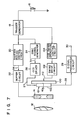
- FIG. 2 there is schematically illustrated an electronic still camera with a solid state image sensor which is a first embodiment of the present invention.
- An interline transfer type charge coupled device (IT-CCD) 10 is provided as the solid state image sensor of this electronic still camera.
- the IT-CCD 10 receives incident image light (not shown) through a lens 12 and a shutter mechanism 14 operable with a high shutter speed of 1/30 sec or less, for example, 1/1000 sec.
- a release button 16 is connected between a trigger generating circuit 18 and ground.
- the trigger generator 18 is connected to the shutter mechanism 14 through a shutter period control circuit 20 for controlling the opening and closing of the shutter mechanism 14 and a buffer circuit 22.
- the trigger generator 18 is electrically connected to the IT-CCD 10 through a sync signal generating circuit 24, a CCD driver 26 and a gate terminal 27.
- An image sensing signal 28 from the IT-CCD 10 is supplied to an output terminal 30 through a signal processing circuit 29 containing an amplifier (not shown).
- the CCD driver 26 drives the IT-CCD 10 in response to a sync signal 31 generated by the sync signal generating circuit 24.
- the IT-CCD 10 is provided, as shown in Fig. 3, with a photosensitive portion 32 made up of photosensitive elements, for example, photodiodes P 11 , P 11 ', P 12 , P 12 ', ..., P 1N , P 1N ', ..., P ij , P ij ', ..., P MN , P MN '.
- photodiodes P vertically arranged, the adjacent photodiodes are paired and designated by paired notation, as just above. This is done for making the notation of the photodiodes arrayed comply with the conventional one adaptable for NTSC system.
- These photodiodes P are arrayed on a CCD substrate (not shown) in a matrix fashion.
- each column includes photodiodes of 2N and the columns of M are arrayed side by side.
- M vertical CCDs C 1 to C r1 are disposed adjacent to the M photodiodes columns, respectively.
- the number of vertical CCDs C 1 to C M is equal to the number of vertical picture elements in the IT-CCD 10, that is, the half (N) of the number of photodiodes contained in each photodiode column.
- the vertical CCDs C 1 to C M are connected at their final transfer stage to a horizontal CCD shift register S.
- a field shift gate (FSG) 34 is arranged with the gate portions each extending through gaps between the vertical photodiode columns P 1 to P M and the vertical CCDs C 1 to C M .
- the FSG 34 is electrically connected to the gate terminal 19.
- a pulse signal (a gate control signal) is applied from the CCD driver 20 to the FSG 34 through the gate terminal 27, the signal charge stored in the photodiodes P is transferred to the vertical CCDs C 1 to C M .
- the signal charge transferred to the vertical CCDs C l to C M is sequentially transferred to the horizontal CCD shift register S for each stage. The charge is then read out from the output terminal 30 through the signal processor 29.
- Fig. 4 shows an enlarged plan view of an image sensing area corresponding to one picture element or one cell in the photosensitive portion 32 of the IT-CCD 10 in Fig. 3.
- a hatched portion 38 indicates an aluminum electrode serving to shut off the incident light.
- the A l electrode 38 has an opening 40 under which the photodiode Pij' is located.
- the vertical CCD C i and the FSG 34 run under the Al electrode 38, and hence are optically shielded from light rays by the Al electrode 38.
- An internal interconnection pattern (not shown) for driving the vertical CCD C i is formed under an area 42 of the Al electrode 38 located above the photodiode Pij.
- the area 42 of the Al electrode 38 performs optical isolation between the photodiodes Pij and Pij'.
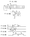
- Fig. 5A shows a waveform of a gate control signal supplied from the CCD driver 26 to the FSG 34 of the IT-CCD 10, through the gate terminal 27.
- the gate control signal has a pulse waveform changing stepwise between a low potential level V L and a high potential level V H , as depicted in Fig. 5A.
- the signal charge generated and stored in the photosensitive section 32 is transferred to the vertical CCDs C 1 to C M , by applying a high potential level V H to the FSG 34 of the IT-CCD 10 within one frame period t F .
- the high potential pulses 50 and 52 shown in Fig. 5A are repeatedly supplied to the FSG 34 of the IT-CCD 10 for every field t f .
- the electronic still camera as a first embodiment of the present invention, at least two pulses 50 and 52 are sufficient for obtaining an instantaneous still image.
- the pulse width T s of each of these pulses 50 and 52 corresponds to a transfer period of the signal charge from the photosensitive section 32 of the IT-CCD 10 to the vertical CCDs C l to C M .
- the pulse width T s ranges from 1 ⁇ sec to 10 ⁇ sec, for example.
- Fig. 5B shows a waveform of a shutter control signal 54 generated by the shutter period control circuit 20 for controlling the opening and closing of the shutter mechanism 14 of Fig. 2.
- the shutter mechanism 14 is operated under control of the pulse signal 54. It should be noted that a center point of the high potential level holding time To of the pulse signal 54 is made coincident with the trailing edge of the pulse component 50 of the gate control signal of Fig. 5A.
- the shutter period control circuit 20 and the sync signal generating circuit 24 are synchronized with each other by the trigger generator 18 so that the application of the high potential of the gate control signal of Fig. 5A to the FSG 34 of the IT-CCD 10 is completed when the shutter mechanism 14 opens and then half of the entire opening time elapses.
- the photosensitive section 32 of the IT-CCD 10 is still irradiated with the image light, and the signal charge generated in the photosensitive section 32 of the IT-CCD 10 is transferred into the vertical CCDs C 1 to C M within the period T s .
- the opening period of the shutter mechanism 14 is centered at the trailing edge of the high potential pulse applied to the FSG 34 of the IT-CCD 10 and ranges to the periods adjacent to that trailing edge, i.e., the above fields A and B. Therefore, in the first half period TO/2 of the shutter opening period T O ,the image light corresponding to the field A image is incident on the photosensitive section 32 of the IT-CCD 10. As a result, the signal charges representing the field A image are generated and stored in the photosensitive section 32. The signal charges of the field A respond to the high potential pulse 50 in the gate control signal of Fig. 5A applied to the FSG 34 of the IT-CCD 10 and are transferred to the vertical CCDs C 1 to C M .
- the image light corresponding to the field B image is applied to the IT-CCD 10, so that the signal charges representing the field B image are stored in the CCD photosensitive section 32.
- the signal charges of the field B respond to the high potential pulse 52 to be transferred to the vertical CCDs C l to C M .
- one-frame image signal is obtained composed of a field A image signal S A and a field B image signal S B , which are at substantially the same signal level, as shown in Fig. 5C.
- the time length of the light irradiation to the IT-CCD 10 during the field A period is equal to that during the field B period, these fields making one frame. Therefore, the output levels of the two fields' (A and B) image signals S A and S B are substantially equal to each other.
- the image sensing apparatus employs a new and unique system for image sensing wherein the shutter is open over a period of the high potential V H applied to the FSG of the IT-CCD, to allow the image light to be applied to the CCD.
- the signals of both the fields A and B can be produced even at a high speed operation such as 1/1000 second, for example. Therefore, the image sensing apparatus according to the present invention may be preferably applied to an electronic still camera without degrading the resolution.
- T S of the V H application pulse is approximately 1 usec, if the shutter opening period To is 1/1000 sec (1 msec), for example, T S is approximately 0.1 % of the shutter opening period T O , and extremely short. Therefore, a slight displacement between the trailing edge of the V H application pulse and the center of the shutter opening period is not problematic.
- Fig. 6 shows a modification of the control for the shutter operation of the shutter mechanism 14 (Fig. 2).
- Fig. 6A shows a waveform of a gate control signal supplied from the CCD driver 26 to the FSG 34 of the IT-CCD 10, and is equal to that of Fig. 5A.
- Fig. 6B shows a pulse waveform of a shutter control signal from the shutter time control circuit 20.
- the shutter control signal has two pulse components 60 and 62 for one operation of a release button 16 (for sensing a single still image).
- the pulse components 60 and 62 appear separated from each other by a predetermined period T M with respect to the center of the high potential pulse generating period T S of the gate control signal of Fig. 6A.
- these pulse components 60 and 62 are produced within the period corresponding to the different successive field periods of one frame period.
- the shutter mechanism (Fig. 2) responds to the shutter control signal to open twice in response to one operation of the release button 16.
- the shutter control signal is generated by the shutter period control circuit 20 on the basis of the operation of the trigger generator 18 and is supplied to the shutter mechanism 14 through the buffer circuit 22. Therefore, the shutter mechanism 14 first opens during a period T ol shown in Fig.
- this period is contained in one of the two periods forming one frame, for example, the field A), thereby allowing the incident light to be applied to the IT-CCD 10.
- the shutter mechanism 14 closes.
- the period T S for applying the high potential V H to the FSG 34 of the IT-CCD 10 is contained in this period T M .
- the signal charge field A image signal
- the shutter mechanism 14 responds to the pulse component 62 to open again.
- the shutter mechanism 14 opens as the second time during a short period as shown in Fig.
- the image light is again applied to the IT-CCD 10 to pick up the field B image.
- the signal charges stored in the photosensitive section 32 of the IT-CCD 10 corresponding to the field B image is transferred as the second time signal to the vertical CCDs C 1 to C M , through the FSG 34 operating in response to the pulse component 52 next generated in Fig. 6A.
- the image signals of the two fields A and B are obtained as shown in Fig. 6C.
- the shutter speed of the first photographing is determined based on the entire period T o ' from a start point of the first shutter opening period to an end point of the second shutter opening period.
- the above modification also allows a high speed shuttering operation of the image sensing apparatus without suffering from a reduction of resolution.
- a shutter closing period i.e., the incident light prohibiting period T M is provided within the shutter open period T o ' for the first photographing of a still picture (T M ⁇ T o ').
- the high potential pulse 50 supplied to the FSG 34 of the IT-CCD 10 is generated.
- the signal charge transfer from the photosensitive section 32 of the IT-CCD 10 to the vertical CCDs C 1 to C M is performed within this perid T M .
- the present invention can attain a high shuttering speed operation with a high resolution.
- the present invention is adaptable for a system for improving a horizontal resolution. This will be described in detail.
- Fig. 7 there is shown an arrangement of an electronic still camera which is another embodiment of the present invention.
- the IT-CCD 10 is so arranged as to vibrate or swing with respect to image light coming through the lens 12 and the shutter mechanism 14.
- the IT-CCD 10 is fixed to a CCD support table 100 on the surface 10b as the reverse side of the image sensing surface 10a of the IT-CCD 10.
- the CCD support table 100 vibrates in a plane orthogonal to incident image light 16 directed toward the IT-CCD 10 by a swing drive circuit 102, in a predetermined direction, e.g., the horizontal direction of the IT-CCD 10, at periods of one frame. Therefore, the IT-CCD 10 fixed to the support table 100 also vibrates or swings relative to the incident image light according to the swing mode.
- a CCD swing operation control circuit 104 provided between the trigger generator 18 and the swing drive circuit 102 responds to a trigger signal generated from the trigger generator 18 interlocked with the release button 16, which is operated for taking a still picture, and properly controls the start of the swing operation of the CCD support table 100.
- Fig. 8A schematically illustrates a plurality of one-cell areas shown in Fig. 4 for purposes of explaining the swing mode of the IT-CCD 10.
- the IT-CCD 10 swings or vibrates in an X-axial direction (horizontal direction) as indicated by an arrow 108 one time for one photographing operation of a still picture, so that the opening 40 with the unit cell Pij of the IT-CCD 10 positioned right thereunder positions at a first photographing position, as indicated by a solid line in Fig. 8A, during the field A period of one frame t F , while it positions at a second position 106 as indicated by a broken line during the field B period t b .
- the vibration mode 8B shows a swing mode called a triangle wave vibration mode of the IT-CCD 10.
- the CCD vibration width in this mode is indicated by a capital letter D. Therefore, if the coordinate of the center of the vibration is 0, the IT-CCD 10 reciprocately moves a distance D/2 in the positive and negative directions with respect to the vibration center 0. Therefore, during the one frame period t F , substantially two spatial sampling areas are present in the horizontal direction of the IT-CCD 10. Therefore, the number of elements of the IT-CCD 10 is effectively doubled, so that the resolution in the horizontal direction is improved two times. While the vibration mode has been described using only the unit cell Pi j for simplicity, the same thing can be correspondingly applied for the remaining cells.
- the signal charges which are generated and stored in the photosensitive section 32 of the swinging IT-CCD 10 during the periods of the fields A and B, are transferred to the vertical CCDs C l to C M at a proper time point during the vertical blanking period.
- the charge transfer period is synchronized with the vibration center of the IT-CCD 10.
- Fig. 9A shows a waveform of a gate control signal supplied to the FSG 34 of the IT-CCD 10.
- a signal waveform shown in Fig. 9A is again illustrated, although it is the same as those shown in Figs. 5A and 6A.
- Fig. 9B shows a waveform of a shutter control signal supplied from the shutter control circuit 20 to the shutter mechanism 14, and is similar to the signal waveform of Fig. 5B.
- Fig. 9C shows a waveform of a drive signal 110 supplied from the drive circuit 102 to the CCD support table 100 for swinging the IT-CCD 10. As seen from Figs.
- a still image of one frame is formed by composing the image outputs of the fields A and B, denoted as S A and S B , which are thus formed (see Fig. 9D).
- the horizontal resolution as well as the vertical resolution can be improved even in the high speed mode by horizontally moving the solid state image sensing chip.
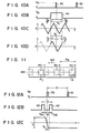
- Fig. 10 shows a set of waveforms for illustrating a modification of the CCD swing technique shown in Fig. 9.
- Figs. 10A and 10B show the same waveforms as those of Figs. 9A and 9B.
- the IT-CCD 10 is driven so as to swing once for a single photographing operation in synchronism with the shutter opening period To.
- the CCD is vibrated before the shutter opening and is continued after the shutter is closed, as seen from Fig. 10C.
- the shutter can be opened while the CCD is stably vibrated, thereby simplifying the coincidence of the center of the shutter opening period and the vibration center.
- Fig. 11 shows a modification of another embodiment of the present invention shown in Figs. 7 to 9.
- the IT-CCD 10 is so designed that it moves in a predetermined direction, for example, the horizontal direction of the CCD as indicated by an arrow 120.
- the IT-CCD 10 is moved when a still picture is taken, so as to satisfy the following equation.
- P H is a horizontal pitch of the photocell Pij of the IT-CCD 10
- L A is a horizontal length of the opening 40 of the cell P ij
- V S is a linear movement speed of the IT-CCD 10.
- Openings 40-1, 40-2, 40-3, ... of the picture element cell Pij are moved up to positions 122 as indicated by broken lines in Fig. 11, i.e., positions of the openings of the cells horizontally adjacent to each other.
- the Fig. 11 embodiment is free from the problem of degradation of the resolution arising from a phase difference, which is generated in the modification of Fig. 10.
- all a designer has to do is to merely change the linear movement speed V s corresponding to the change in shutter speed.
- Figs. 12A 'to 12C show waveforms of the gate control signal, the shutter control signal and the vibration mode of the IT-CCD in the modification of the electronic still camera as described referring to Fig. 6.
- the waveforms of Figs. 12A and 12B are the same as those in Figs. 6A and 6B, respectively, which are again illustrated for ease of explanation.
- the IT-CCD 10 stops at a first position and receives the incident image light.
- the IT-CCD 10 moves at a constant speed in a given direction, e.g., a horizontal direction of the CCD, or in a direction corresponding to a slant direction on the reproduced picture, and reaches a second position immediately before the shutter closing period T M .
- the IT-CCD 10 stops at the second position again to receive the incident image light.
- the moving period of the CCD T c is set to be smaller than the shutter closing time T M , T c ⁇ T M .
- a distance between the first and second positions, that is, a moving distance d within the shutter closing period Tp Z of the IT-CCD 10 is selected like the distance D shown in Fig.
- the IT-CCD 10 displaces from the second position to the first position, as in the previous case.
- the solid state image sensing device applied to the present invention is not limited by the IT-CCD used in the embodiments mentioned above, but may be obviously replaced by any means if it can store the signal charges generated in the photosensitive section of each picture element for a given period and then transfer the signal changes to the readout section.
- the present invention is applicable for a so-called multi-layered sensor in which the photo-electric conversion is performed by use of the photoconductive film, and the readout of the signal charges is made using the conventional solid state image pick-up element. While the embodiment of Fig. 3 employs an array of photodiodes in which the photodiodes are vertically arranged in a line, these may be arranged in a zig-zag fashion.
- a couple of high potential pulses are generated in succession for the gate control signal supplied to the FSG of the IT-CCD, as shown in Fig. 12A. If a plurality of high potential pulses V H are applied at time points before and after the pulse pair, the present invention can be practiced with substantially the same effect.
- the present invention is applicable for an electronic still camera with one, two or three solid image sensing chip substrates for effecting the color image pick-up.
- a reproduced picture with a high resolution can be obtained if the image sensing apparatus according to the present invention and the picture element displacing method are combined in the electronic camera with the two or three chip substrates.
- a one-dimensional sensor may be used to improve the resolution.
- the number of the photodiodes in the vertical direction is two times that of the stages of the CCD.
- the present invention is also applicable to a case where the number of stages of both the elements are equal to each other.
- the solid state image sensing chip substrate is relatively moved in the direction corresponding to the horizontal direction on the reproduced picture. It is evident that the it may also be moved diagonally.
- the vibration mode of the IT-CCD 10 may be not only the triangle wave vibration mode, but also a sinusoidal wave vibration mode, a trapezoidal vibration mode, a step vibration mode or the like.
Landscapes
- Engineering & Computer Science (AREA)
- Multimedia (AREA)
- Signal Processing (AREA)
- Transforming Light Signals Into Electric Signals (AREA)
- Solid State Image Pick-Up Elements (AREA)
Applications Claiming Priority (2)
| Application Number | Priority Date | Filing Date | Title |
|---|---|---|---|
| JP57051418A JPS58169966A (ja) | 1982-03-31 | 1982-03-31 | 固体撮像装置の駆動方式 |
| JP51418/82 | 1982-03-31 |
Publications (3)
| Publication Number | Publication Date |
|---|---|
| EP0090597A2 true EP0090597A2 (fr) | 1983-10-05 |
| EP0090597A3 EP0090597A3 (en) | 1986-01-02 |
| EP0090597B1 EP0090597B1 (fr) | 1989-07-26 |
Family
ID=12886375
Family Applications (1)
| Application Number | Title | Priority Date | Filing Date |
|---|---|---|---|
| EP83301634A Expired EP0090597B1 (fr) | 1982-03-31 | 1983-03-23 | Dispositif électronique pour capter des images |
Country Status (4)
| Country | Link |
|---|---|
| US (1) | US4535363A (fr) |
| EP (1) | EP0090597B1 (fr) |
| JP (1) | JPS58169966A (fr) |
| DE (1) | DE3380288D1 (fr) |
Cited By (1)
| Publication number | Priority date | Publication date | Assignee | Title |
|---|---|---|---|---|
| GB2208773A (en) * | 1987-08-14 | 1989-04-12 | Tamfelt Oy Ab | A method of taking pictures of a quick-moving object |
Families Citing this family (20)
| Publication number | Priority date | Publication date | Assignee | Title |
|---|---|---|---|---|
| JPS59174074A (ja) * | 1983-03-23 | 1984-10-02 | Toshiba Corp | 固体撮像装置の出力信号再生回路 |
| US4652928A (en) * | 1983-06-15 | 1987-03-24 | Kabushiki Kaisha Toshiba | Solid state image sensor with high resolution |
| JPS60160270A (ja) * | 1984-01-31 | 1985-08-21 | Toshiba Corp | 固体撮像装置 |
| JPH0640665B2 (ja) * | 1984-04-13 | 1994-05-25 | 株式会社東芝 | 固体撮像装置の出力信号再生回路 |
| JPH07114472B2 (ja) * | 1984-11-19 | 1995-12-06 | 株式会社ニコン | 固体撮像素子の駆動方法 |
| EP0196009A3 (fr) * | 1985-03-20 | 1987-01-14 | Casio Computer Company Limited | Caméra pour vues fixes |
| JPS6266468U (fr) * | 1985-10-16 | 1987-04-24 | ||
| US4748507A (en) * | 1986-10-17 | 1988-05-31 | Kenneth Gural | Solid state imaging device having means to shift the image between scans and associated circuitry to improve the scanned image |
| DE3877034T2 (de) * | 1987-04-10 | 1993-04-22 | Toshiba Kawasaki Kk | Festkoerper-bildabtaster mit hochgeschwindigkeitsverschluss und verfahren zur erzielung einer hohen verschlussgeschwindigkeit in einem festkoerper-bildabtaster. |
| GB8709916D0 (en) * | 1987-04-27 | 1987-10-21 | Gec Avionics | Imaging systems |
| JP3318437B2 (ja) * | 1994-05-26 | 2002-08-26 | 富士写真フイルム株式会社 | 電子スチルカメラの撮像素子遮蔽装置 |
| JPH0832879A (ja) * | 1994-07-14 | 1996-02-02 | Fuji Photo Film Co Ltd | 画像読取方法 |
| US5754228A (en) * | 1995-09-25 | 1998-05-19 | Lockhead Martin Corporation | Rapid-sequence full-frame CCD sensor |
| JP3617887B2 (ja) * | 1996-10-14 | 2005-02-09 | シャープ株式会社 | 撮像装置 |
| US6251086B1 (en) * | 1999-07-27 | 2001-06-26 | Scimed Life Systems, Inc. | Guide wire with hydrophilically coated tip |
| JP3704238B2 (ja) * | 1997-03-31 | 2005-10-12 | 株式会社リコー | 撮像装置 |
| JP3988215B2 (ja) * | 1997-07-17 | 2007-10-10 | 株式会社ニコン | 撮像装置 |
| BG107215A (bg) * | 2002-10-23 | 2004-04-30 | Melexis Nv Microelectronic Integrated Systems | Сигнализиращо средство за сензорни многоелементни системи |
| JP5328526B2 (ja) * | 2009-07-03 | 2013-10-30 | キヤノン株式会社 | 撮像装置 |
| US9204129B2 (en) * | 2010-09-15 | 2015-12-01 | Perceptron, Inc. | Non-contact sensing system having MEMS-based light source |
Citations (2)
| Publication number | Priority date | Publication date | Assignee | Title |
|---|---|---|---|---|
| JPS5651169A (en) * | 1979-10-02 | 1981-05-08 | Fuji Photo Film Co Ltd | Light emission controlling method of strobe light |
| FR2486387A1 (fr) * | 1980-07-11 | 1982-01-15 | Siemens Ag | Installation de radiodiagnostic a convertisseur d'image a l'etat solide |
Family Cites Families (8)
| Publication number | Priority date | Publication date | Assignee | Title |
|---|---|---|---|---|
| US3824336A (en) * | 1972-03-17 | 1974-07-16 | Teletronics Int Inc | Editing system and method |
| US4057830A (en) * | 1972-06-27 | 1977-11-08 | Texas Instruments Incorporated | Electronic photography system |
| GB1577026A (en) * | 1977-05-18 | 1980-10-15 | Rank Organisation Ltd | Telecine apparatus |
| US4131919A (en) * | 1977-05-20 | 1978-12-26 | Eastman Kodak Company | Electronic still camera |
| US4161000A (en) * | 1977-10-28 | 1979-07-10 | Video Systems Research, Inc. | High speed television camera control system |
| JPS5562423A (en) * | 1978-11-02 | 1980-05-10 | Olympus Optical Co Ltd | Projecting device |
| JPS5668068A (en) * | 1979-11-09 | 1981-06-08 | Toshiba Corp | Image pickup system using electric charge transfer element |
| US4471388A (en) * | 1981-12-14 | 1984-09-11 | Rca Corporation | Television camera mechanical apparatus driven by recorder motor |
-
1982
- 1982-03-31 JP JP57051418A patent/JPS58169966A/ja active Granted
-
1983
- 1983-03-23 DE DE8383301634T patent/DE3380288D1/de not_active Expired
- 1983-03-23 EP EP83301634A patent/EP0090597B1/fr not_active Expired
- 1983-03-23 US US06/478,104 patent/US4535363A/en not_active Expired - Lifetime
Patent Citations (2)
| Publication number | Priority date | Publication date | Assignee | Title |
|---|---|---|---|---|
| JPS5651169A (en) * | 1979-10-02 | 1981-05-08 | Fuji Photo Film Co Ltd | Light emission controlling method of strobe light |
| FR2486387A1 (fr) * | 1980-07-11 | 1982-01-15 | Siemens Ag | Installation de radiodiagnostic a convertisseur d'image a l'etat solide |
Non-Patent Citations (2)
| Title |
|---|
| APPLIED OPTICS, vol. 21, no. 5, March 1, 1982, pages 851-860, New York, US; B.L. GOTWOLS et al.: "Charge-coupled device camera system for remotely measuring the dynamics of ocean waves" * |
| PATENTS ABSTRACTS OF JAPAN, vol. 5, no. 113 (E-66)(785), July 22, 1981; & JP - A - 56 051 169 (FUJI SHASHIN FILM K.K.) 08-05-1981 * |
Cited By (1)
| Publication number | Priority date | Publication date | Assignee | Title |
|---|---|---|---|---|
| GB2208773A (en) * | 1987-08-14 | 1989-04-12 | Tamfelt Oy Ab | A method of taking pictures of a quick-moving object |
Also Published As
| Publication number | Publication date |
|---|---|
| US4535363A (en) | 1985-08-13 |
| JPS58169966A (ja) | 1983-10-06 |
| EP0090597A3 (en) | 1986-01-02 |
| EP0090597B1 (fr) | 1989-07-26 |
| JPH0454429B2 (fr) | 1992-08-31 |
| DE3380288D1 (en) | 1989-08-31 |
Similar Documents
| Publication | Publication Date | Title |
|---|---|---|
| EP0090597B1 (fr) | Dispositif électronique pour capter des images | |
| US4541016A (en) | Solid state image pickup device | |
| US4998164A (en) | Swing-driven solid-state color image sensor | |
| CN1036233C (zh) | 视频信号处理设备 | |
| EP0150973B2 (fr) | Capteur d'images avec mouvements oscillatoires et vibratoires | |
| EP0859509B1 (fr) | Méthode de surveillance avec un dispositif d'imagerie CCD et caméra numérique à image fixe utilisant ce procédé | |
| JPH08223465A (ja) | 順次走査撮像センサ上の画像の高速自動焦点調節を備える電子カメラ | |
| JP2753541B2 (ja) | 静止画撮像装置 | |
| WO1997017811A1 (fr) | Procede et dispositif pour la prise de vue d'image fixe en couleur | |
| EP0195270B1 (fr) | Caméra vidéo | |
| US4499496A (en) | Solid state image sensing device | |
| EP0421243B1 (fr) | Caméra à mise au point automatique | |
| US4734773A (en) | Imaging apparatus having high-frequency electron purging circuit operable during an exposure time | |
| JPH0140547B2 (fr) | ||
| EP0568216A1 (fr) | Dispositif de prise de vues à l'état solide | |
| JP2809937B2 (ja) | Ccd撮像装置 | |
| JPH08307776A (ja) | 撮像装置 | |
| JPS6350172A (ja) | ビデオカメラ装置 | |
| JPH04257171A (ja) | 撮像装置 | |
| JPS63101811A (ja) | 電子カメラの自動焦点調節装置 | |
| JPH04167776A (ja) | 撮像装置及び固体撮像素子の駆動装置 | |
| JPS6027279A (ja) | 画像読取方法 | |
| JPS61264874A (ja) | 固体撮像装置 | |
| JPH0955885A (ja) | 撮像装置 | |
| JPH04343586A (ja) | 固体撮像素子の駆動方法 |
Legal Events
| Date | Code | Title | Description |
|---|---|---|---|
| PUAI | Public reference made under article 153(3) epc to a published international application that has entered the european phase |
Free format text: ORIGINAL CODE: 0009012 |
|
| 17P | Request for examination filed |
Effective date: 19830330 |
|
| AK | Designated contracting states |
Designated state(s): DE FR GB NL |
|
| RAP1 | Party data changed (applicant data changed or rights of an application transferred) |
Owner name: KABUSHIKI KAISHA TOSHIBA |
|
| PUAL | Search report despatched |
Free format text: ORIGINAL CODE: 0009013 |
|
| AK | Designated contracting states |
Designated state(s): DE FR GB NL |
|
| 17Q | First examination report despatched |
Effective date: 19880229 |
|
| GRAA | (expected) grant |
Free format text: ORIGINAL CODE: 0009210 |
|
| AK | Designated contracting states |
Kind code of ref document: B1 Designated state(s): DE FR GB NL |
|
| REF | Corresponds to: |
Ref document number: 3380288 Country of ref document: DE Date of ref document: 19890831 |
|
| ET | Fr: translation filed | ||
| PLBE | No opposition filed within time limit |
Free format text: ORIGINAL CODE: 0009261 |
|
| STAA | Information on the status of an ep patent application or granted ep patent |
Free format text: STATUS: NO OPPOSITION FILED WITHIN TIME LIMIT |
|
| 26N | No opposition filed | ||
| REG | Reference to a national code |
Ref country code: GB Ref legal event code: 746 Effective date: 19981126 |
|
| PGFP | Annual fee paid to national office [announced via postgrant information from national office to epo] |
Ref country code: DE Payment date: 19991231 Year of fee payment: 18 |
|
| PGFP | Annual fee paid to national office [announced via postgrant information from national office to epo] |
Ref country code: FR Payment date: 20000310 Year of fee payment: 18 |
|
| PGFP | Annual fee paid to national office [announced via postgrant information from national office to epo] |
Ref country code: GB Payment date: 20000322 Year of fee payment: 18 |
|
| PGFP | Annual fee paid to national office [announced via postgrant information from national office to epo] |
Ref country code: NL Payment date: 20000330 Year of fee payment: 18 |
|
| REG | Reference to a national code |
Ref country code: FR Ref legal event code: D6 |
|
| PG25 | Lapsed in a contracting state [announced via postgrant information from national office to epo] |
Ref country code: GB Free format text: LAPSE BECAUSE OF NON-PAYMENT OF DUE FEES Effective date: 20010323 |
|
| PG25 | Lapsed in a contracting state [announced via postgrant information from national office to epo] |
Ref country code: NL Free format text: LAPSE BECAUSE OF NON-PAYMENT OF DUE FEES Effective date: 20011001 |
|
| GBPC | Gb: european patent ceased through non-payment of renewal fee |
Effective date: 20010323 |
|
| PG25 | Lapsed in a contracting state [announced via postgrant information from national office to epo] |
Ref country code: FR Free format text: LAPSE BECAUSE OF NON-PAYMENT OF DUE FEES Effective date: 20011130 |
|
| NLV4 | Nl: lapsed or anulled due to non-payment of the annual fee |
Effective date: 20011001 |
|
| REG | Reference to a national code |
Ref country code: FR Ref legal event code: ST |
|
| PG25 | Lapsed in a contracting state [announced via postgrant information from national office to epo] |
Ref country code: DE Free format text: LAPSE BECAUSE OF NON-PAYMENT OF DUE FEES Effective date: 20020101 |