EP0083542A1 - Sélecteur de longueurs d'ondes - Google Patents
Sélecteur de longueurs d'ondes Download PDFInfo
- Publication number
- EP0083542A1 EP0083542A1 EP82402383A EP82402383A EP0083542A1 EP 0083542 A1 EP0083542 A1 EP 0083542A1 EP 82402383 A EP82402383 A EP 82402383A EP 82402383 A EP82402383 A EP 82402383A EP 0083542 A1 EP0083542 A1 EP 0083542A1
- Authority
- EP
- European Patent Office
- Prior art keywords
- concave mirror
- plane
- reflecting device
- layer
- mirror
- Prior art date
- Legal status (The legal status is an assumption and is not a legal conclusion. Google has not performed a legal analysis and makes no representation as to the accuracy of the status listed.)
- Granted
Links
Images

Classifications
-
- G—PHYSICS
- G02—OPTICS
- G02B—OPTICAL ELEMENTS, SYSTEMS OR APPARATUS
- G02B6/00—Light guides; Structural details of arrangements comprising light guides and other optical elements, e.g. couplings
- G02B6/24—Coupling light guides
- G02B6/26—Optical coupling means
- G02B6/28—Optical coupling means having data bus means, i.e. plural waveguides interconnected and providing an inherently bidirectional system by mixing and splitting signals
- G02B6/293—Optical coupling means having data bus means, i.e. plural waveguides interconnected and providing an inherently bidirectional system by mixing and splitting signals with wavelength selective means
- G02B6/29304—Optical coupling means having data bus means, i.e. plural waveguides interconnected and providing an inherently bidirectional system by mixing and splitting signals with wavelength selective means operating by diffraction, e.g. grating
- G02B6/29305—Optical coupling means having data bus means, i.e. plural waveguides interconnected and providing an inherently bidirectional system by mixing and splitting signals with wavelength selective means operating by diffraction, e.g. grating as bulk element, i.e. free space arrangement external to a light guide
- G02B6/29307—Optical coupling means having data bus means, i.e. plural waveguides interconnected and providing an inherently bidirectional system by mixing and splitting signals with wavelength selective means operating by diffraction, e.g. grating as bulk element, i.e. free space arrangement external to a light guide components assembled in or forming a solid transparent unitary block, e.g. for facilitating component alignment
-
- G—PHYSICS
- G02—OPTICS
- G02B—OPTICAL ELEMENTS, SYSTEMS OR APPARATUS
- G02B6/00—Light guides; Structural details of arrangements comprising light guides and other optical elements, e.g. couplings
- G02B6/24—Coupling light guides
- G02B6/26—Optical coupling means
- G02B6/28—Optical coupling means having data bus means, i.e. plural waveguides interconnected and providing an inherently bidirectional system by mixing and splitting signals
- G02B6/293—Optical coupling means having data bus means, i.e. plural waveguides interconnected and providing an inherently bidirectional system by mixing and splitting signals with wavelength selective means
- G02B6/29346—Optical coupling means having data bus means, i.e. plural waveguides interconnected and providing an inherently bidirectional system by mixing and splitting signals with wavelength selective means operating by wave or beam interference
- G02B6/29361—Interference filters, e.g. multilayer coatings, thin film filters, dichroic splitters or mirrors based on multilayers, WDM filters
- G02B6/29368—Light guide comprising the filter, e.g. filter deposited on a fibre end
-
- G—PHYSICS
- G02—OPTICS
- G02B—OPTICAL ELEMENTS, SYSTEMS OR APPARATUS
- G02B6/00—Light guides; Structural details of arrangements comprising light guides and other optical elements, e.g. couplings
- G02B6/24—Coupling light guides
- G02B6/26—Optical coupling means
- G02B6/28—Optical coupling means having data bus means, i.e. plural waveguides interconnected and providing an inherently bidirectional system by mixing and splitting signals
- G02B6/293—Optical coupling means having data bus means, i.e. plural waveguides interconnected and providing an inherently bidirectional system by mixing and splitting signals with wavelength selective means
- G02B6/29379—Optical coupling means having data bus means, i.e. plural waveguides interconnected and providing an inherently bidirectional system by mixing and splitting signals with wavelength selective means characterised by the function or use of the complete device
- G02B6/2938—Optical coupling means having data bus means, i.e. plural waveguides interconnected and providing an inherently bidirectional system by mixing and splitting signals with wavelength selective means characterised by the function or use of the complete device for multiplexing or demultiplexing, i.e. combining or separating wavelengths, e.g. 1xN, NxM
Definitions
- the present invention relates to a selector for separating two wavelength ranges in complex light. It applies more particularly to the multiplexing or separation of information transmitted by optical fibers.
- multi-electric layers consisting of a superposition of thin layers, of the order of a quarter of the wavelength of the light concerned, and alternatively in materials of high and low index, such as example of zinc sulfide or cryolite.
- an overall layer is obtained which, relative to a critical wavelength, reflects the wavelengths longer, for example, at this critical value ⁇ o while it lets through. the lower wavelengths.
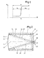
- FIG. 1 the simplified graph of FIG. 1 where the light energy collected after reflection by a multi-electric layer of a light beam emitting in a wide spectral band A has been represented on the y-axis.
- the reflected light is almost zero while in the band A 2 whose wavelengths are greater than ⁇ o the light is almost fully reflected.
- the dielectric layer therefore behaves like a mirror for the strip A 2 and like a transparent strip for the strip A 1 .
- the invention constitutes a new application of a multi-electric layer for separating, in a light introduced into the selector by an input optical fiber, two different bands of wavelengths and collecting them separately on at least two other optical fibers of exit.
- the invention relates to a selector for separating at least two ranges of wavelengths in complex light introduced into the apparatus by the end of an optical fiber placed in the immediate vicinity of the focal point of a concave mirror producing a parallel beam directed towards a plane reflecting device, the return beam being focused towards an optical output fiber.
- the device comprises at least one plane multi-electric layer interposed between the concave mirror and the planar reflecting device and forming with the axis at the top of the concave mirror an angle slightly different from that of the planar reflecting device, each layer multi-electric having an interruption in the vicinity of the axis at the top of the concave mirror.
- the plane reflecting device is a plane mirror.
- the reflecting device is a plane grating of diffraction by reflection.
- Figure 2 shows a device for simply separating two wavelength bands.
- FIG. 3 shows a device also operating as a monochromator in a band of wavelengths.
- the device consists of the juxtaposition of two glass blocks 1 and 2.
- the block 1 has a spherical or parabolic convex part 4.
- the surface 4 is made reflective by a coating 5 which thus constitutes, towards the inside of the block, a concave mirror whose main axis 6 is normal to the top of the surface 4.
- the coating 5 is interrupted on a small central area 7 in the vicinity of the top of the convex part.
- the block 1 has, at the end opposite to the surface 4, a flat surface on which the second block 2 is bonded having a flat planar surface.
- This last flat surface carries a multi-electric layer 8, also interrupted in the vicinity of the main axis 6 of the mirror 5.
- the block 2 constitutes a plane mirror 10 perpendicular to the axis 6 and arranged in the focal plane of the mirror. concave 5.
- the end of the input optical fiber 12 is flush with the surface of the plane mirror 10 and is very slightly offset from the focal point of the mirror 5.
- the beam 14 from the end of the fiber 12 passes into the area where the layer 8 is interrupted and is reflected on the mirror 5 in a parallel beam 15.
- the beam 15 of spectral width A (FIG. 1)
- the strip A 1 crosses the layer 8 and is reflected on the mirror 10 in a beam parallel 16 which again crosses the layer 8; by reflection on the mirror 5 it becomes the beam 17 which focuses at a point slightly offset from the focus of the mirror 5 and where it is collected by the output fiber 18.
- the spectral band A 2 does not cross the layer 8, but the latter reflects it like a plane mirror in a new parallel beam 20 angularly offset as a function of the angle of the layer 8 in relation to the axis 6.
- the beam 20 is reflected in a beam 21 which is focused on the end of another output fiber 22.
- the layer 8 by its structure and its inclination relative to the axis 6, separates the two bands A 1 and A 2 from the overall band A and, by modifying the angular direction of one, makes it possible to collect on the two separate fibers 18 and 22.
- the non-reflecting zone 7 makes it possible to eliminate the rays coming from the input fiber 12 and which could have directly reached the output fibers 18 and 22 without being filtered by the layer 8.
- the multi-electric layer 8 is produced by alternating layers of high and low index and of optical thickness approximately ⁇ c being the central wavelength of the range A 2 where the reflective power must be maximum, and in the case of order 0 for the filter thus formed.
- ⁇ c being the central wavelength of the range A 2 where the reflective power must be maximum
- FIG. 4 then represents the reflecting power as a function of the wavelength, and this will reach 0.998 for the range from 8000 to 8800 0 A, while it will be practically zero for the range from 7000 to 7400 A.
- the more complete device of FIG. 3 allows not only the selection of the band A 1 but also, inside the band A 1 , the selection of one or more nonchromatic wavelengths.
- block 32 homologous to block 2 in FIG. 2, is glued to a third block 33 carrying a planar diffraction grating 40.
- the beam 44 coming from the end of the input fiber 42 is reflected in a parallel beam 45 by the mirror 35, with the exception of rays which end at the non-reflecting zone 37.
- the strip A 2 reflected at 50 by the layer 38, and at 51 by the mirror 35, is focused on the output fiber 52.
- the wavelengths of the band A 1 after crossing the layer 38, meet the network 40 which disperses them in different directions.
- one of the wavelengths will be sent back in a parallel beam 46 then reflected in a beam 47 to be focused on the end of the output fiber 48.
- Another wavelength will give the beam 49 which will similarly be focused on another output fiber 54.
- the optical assembly thus formed therefore behaves as a band selector for the band A 2 , and as a monochromator for the wavelengths of the band A l .
- the invention is not strictly limited to the embodiments which have been described by way of example, but it also covers the embodiments which would differ therefrom only in details, in variant embodiments or by the use of equivalent means.
- the focus on the output fiber 18 instead of slightly shifting the input fiber 12 relative to the focus of the mirror 5, it could also be possible for the focus on the output fiber 18 to be distinct from the end of the fiber 12, place this input fiber 12 just at the focus of the concave mirror 5, but give the plane mirror 10 an angle very slightly different from 90 ° relative to the axis 6.
Abstract
Description
- La présente invention concerne un sélecteur pour séparer deux plages de longueurs d'onde dans une lumière complexe. Elle s'applique plus particulièrement au multiplexage ou séparation d'informations transmises par fibres optiques.
- Le développement de la technique de transmission d'informations par modulation de signaux lumineux transmis à longue distance par fibres optiques a conduit à faire transmettre par une même fibre plusieurs signaux portés chacun par des lumières de longueurs d'onde ou de plages de longueurs d'onde différentes. Il est donc important, à l'extrémité de la. fibre, de séparer les diverses plages pour détecter séparément chacun des signaux associés à chaque plage.
- On connait par ailleurs les propriétés des couches multidiélectriques constituées par une superposition de couches minces, d'épaisseur de l'ordre du quart de la longueur d'onde de la lumière concernée, et alternativement en matériaux de fort et de faible indice, comme par exemple du sulfure de zinc ou de la cryolithe. Par un choix convenable du nombre et de l'épaisseur des couches élémentaires on obtient une couche globale qui, relativement à une longueur d'onde critique, réfléchit les longueurs d'onde supérieures par exemple à cette valeur critique λo tandis qu'elle laisse passer les longueurs d'onde inférieures. Ceci est illustré par le graphique simplifié de la figure 1 où l'on a représenté en ordonnées, pour chaque longueur d'onde, l'énergie lumineuse recueillie après réflexion par une couche multidiélectrique d'un faisceau lumineux émettant dans une large bande spectrale A. Dans la bande Al dont les longueurs d'onde sont inférieures à la longueur d'onde critique λo de la couche, la lumière réfléchie est presque nulle tandis que dans la bande A2 dont les longueurs d'onde sont supérieures à λo la lumière est pratiquement entièrement réfléchie. La couche diélectrique se comporte donc comme un miroir pour la bande A2 et comme une lame transparente pour la bande A1.
- L'invention constitue une application nouvelle d'une couche multidiélectrique pour séparer, dans une lumière introduite dans le sélecteur par une fibre optique d'entrée, deux bandes différentes de longueurs d'onde et les recueillir séparément sur au moins deux autres fibres optiques de sortie.
- L'invention concerne un sélecteur pour séparer au moins deux plages de longueurs d'onde dans une lumière complexe introduite dans l'appareil par l'extrémité d'une fibre optique disposée au voisinage immédiat du foyer d'un miroir concave produisant un faisceau parallèle dirigé vers un dispositif réfléchissant plan, le faisceau en retour étant focalisé vers une fibre optique de sortie.
- Selon l'invention l'appareil comporte au moins une couche mulidi- électrique plane interposée entre le miroir concave et le dispositif réfléchissant plan et formant avec l'axe au sommet du miroir concave un angle légèrement différent de celui du dispositif réfléchissant plan, chaque couche multidiélectrique présentant une interruption au voisinage de l'axe au sommet du miroir concave.
- Selon une forme particulière de réalisation de l'invention le dispositif réfléchissant plan est un miroir plan.
- Selon une autre forme de réalisation de l'invention le dispositif réfléchissant est un réseau plan de diffraction par réflexion.
- L'invention sera mieux comprise en se référant aux modes de réalisation particuliers donnés à titre d'exemple et représentés par les autres dessins annexés.
- La figure 2 montre un dispositif destiné à séparer simplement deux bandes de longueurs d'onde.
- La figure 3 montre un dispositif fonctionnant également en monochromateur dans une bande de longueurs d'onde.
- En se référant tout d'abord à la figure 2, on voit que le dispositif est constitué par la juxtaposition de deux blocs de verre 1 et 2. Le bloc 1 présente une partie convexe sphérique ou parabolique 4. La surface 4 est rendue réfléchissante par un revêtement 5 qui constitue ainsi, vers l'intérieur du bloc, un miroir concave dont l'axe principal 6 est la normale au sommet de la surface 4. Le revêtement 5 est interrompu sur une petite zone centrale 7 au voisinage du sommet de la partie convexe. Le bloc 1 présente, à l'extrémité opposée à la surface 4, une surface plane sur laquelle est collé le deuxième bloc 2 présentant une surface plane conjugée. Cette dernière surface plane porte une couche multidiélectrique 8, également interrompue au voisinage de l'axe principal 6 du miroir 5. Sur son autre face le bloc 2 constitue un miroir plan 10 perpendiculaire à l'axe 6 et disposé dans le plan focal du miroir concave 5.
- L'extrémité de la fibre optique d'entrée 12 affleure à la surface du miroir plan 10 et est très légèrement décalée par rapport au foyer du miroir 5. Le faisceau 14 issu de l'extrémité de la fibre 12 passe dans la zone où la couche 8 est interrompue et se réfléchit sur le miroir 5 en un faisceau parallèle 15. Dans le faisceau 15 de largeur spectrale A (figure 1), la bande Al traverse la couche 8 et se réfléchit sur le miroir 10 en un faisceau parallèle 16 qui à nouveau traverse la couche 8;par réflexion sur le miroir 5 il devient le faisceau 17 qui se focalise en un point légèrement décalé par rapport au foyer du miroir 5 et où il est recueilli par la fibre de sortie 18.
- Dans le faisceau parallèle 15 la bande spectrale A2 ne traverse pas la couche 8, mais celle-ci le réfléchit comme un miroir plan en un nouveau faisceau parallèle 20 décalé angulairement en fonction de l'angle de la couche 8 par rappport à l'axe 6. Le faisceau 20 est réfléchi en un faisceau 21 qui est focalisé sur l'extrémité d'une autre fibre de sortie 22.
- On voit que la couche 8, par sa structure et son inclinaison par rapport à l'axe 6, sépare les deux bandes A1 et A2 de la bande globale A et, en modifiant la direction angulaire de l'une, permet de les recueillir sur les deux fibres séparées 18 et 22. On notera que la zone non réfléchissante 7 permet d'éliminer les rayons issus de la fibre d'entrée 12 et qui auraient pu atteindre directement les fibres de sortie 18 et 22 sans être filtrés par la couche 8.
- En pratique on réalise la couche multidiélectrique 8 par une alternance de couches de haut et bas indice et d'épaisseur optique environ λc étant la longueur d'onde centrale de la plage A2 où le pouvoir réflecteur doit être maximum, et dans le cas de l'ordre 0 pour le filtre ainsi constitué. Pour l'ordre 1, qui permet une séparation plus tranchée des bandes, l'épaisseur optique des couches sera

- Ainsi pour séparer une bande A1 de 7000 à 7400 A et une bande A2 de 8000 à 8800 Å, avec des supports 1 et 2 d'indice 1,563 et en travaillant dans l'ordre 1, on utilisera des couches H d'indice 2,35 et d'épaisseur 2625 Å et des couches L d'indice 1,35 et d'épaisseur 4569 Å, la longueur d'onde centrale de la plage A2 étant prise à 8225 Å. La couche 8 comprendra alors une demi-couche H, puis neuf couches L intercalées avec huit couches H, puis à nouveau une demi-couche H.
- La figure 4 représente alors le pouvoir réflecteur en fonction de la longueur d'onde, et celui-ci atteindra 0,998 pour la plage de 8000 à 8800 0 A, tandis qu'il sera pratiquement nul pour la plage de 7000 à 7400 A.
- Le dispositif plus complet de la figure 3 permet non seulement la sélection de la bande A1 mais encore, à l'intérieur de la bande A1, la sélection d'une ou plusieurs longueurs d'onde nonchromatiques.
- Pour celà le bloc 32, homologue du bloc 2 de la figure 2, est collé sur un troisième bloc 33 portant un réseau plan de diffraction 40. Comme dans le cas précédent le faisceau 44 issu de l'extrémité de la fibre d'entrée 42 est réfléchi en un faisceau parallèle 45 par le miroir 35, à l'exception des rayons qui aboutissent à-la zone non réfléchissante 37. Ici encore la bande A2 réfléchie en 50 par la couche 38, et en 51 par le miroir 35, est focalisée sur la fibre de sortie 52.
- Par contre les longueurs d'onde de la bande A1, après traversée de la couche 38, rencontrent le réseau 40 qui les disperse dans des directions différentes. Ainsi par exemple l'une des longueurs d'onde sera.renvoyée en un faisceau parallèle 46 puis réfléchi en un faisceau 47 pour être focalisé sur l'extrémité de la fibre de sortie 48. Une autre longueur d'onde donnera le faisceau 49 qui sera de la même façon focalisé sur une autre fibre de sortie 54. L'ensemble optique ainsi constitué se comporte donc comme un sélecteur de bande pour la bande A2, et comme un monochromateur pour les longueurs d'onde de la bande Al.
- Bien entendu l'invention n'est pas strictement limitée aux modes de réalisation qui ont été décrits à titre d'exemple, mais elle couvre aussi les réalisations qui n'en différeraient que par des détails, par des variantes de réalisation ou par l'utilisation de moyens équivalents. Ainsi dans le cas de la figure 2, au lieu de décaler légèrement la fibre d'entrée 12 par rapport au foyer du miroir 5, on pourrait aussi pour que la focalisation sur la fibre de sortie 18 soit distincte de l'extrémité de la fibre 12, placer cette fibre d'entrée 12 juste au foyer du miroir concave 5, mais donner au miroir plan 10 un angle très légèrement différent de 90° par rapport à l'axe 6.
- On pourrait aussi utiliser plusieurs couches multidiélectriques l'une derrière l'autre avec des angles légèrement différents réalisant ainsi autant de miroirs dichroiques, chaque couche séparant deux plages particulières de longueurs d'onde.
Claims (3)
caractérisé par le fait qu'il comporte au moins une couche multidiélectrique plane (8) interposée entre le miroir concave (5) et le dispositif réfléchissant plan (10) et formant avec l'axe (6) au sommet du miroir concave un angle légèrement différent de celui du dispositif réfléchissant plan, chaque couche multidiélectrique présentant une interruption au voisinage de l'axe au sommet du miroir concave.
caractérisé par le fait que le dispositif réfléchissant plan est un miroir plan (10).
caractérisé par le fait que le dispositif réfléchissant plan est un réseau plan de diffraction par réflexion (40).
Priority Applications (1)
| Application Number | Priority Date | Filing Date | Title |
|---|---|---|---|
| AT82402383T ATE14263T1 (de) | 1981-12-24 | 1982-12-24 | Wellenlaengensortierer. |
Applications Claiming Priority (2)
| Application Number | Priority Date | Filing Date | Title |
|---|---|---|---|
| FR8124211A FR2519148B1 (fr) | 1981-12-24 | 1981-12-24 | Selecteur de longueurs d'ondes |
| FR8124211 | 1981-12-24 |
Publications (2)
| Publication Number | Publication Date |
|---|---|
| EP0083542A1 true EP0083542A1 (fr) | 1983-07-13 |
| EP0083542B1 EP0083542B1 (fr) | 1985-07-10 |
Family
ID=9265391
Family Applications (1)
| Application Number | Title | Priority Date | Filing Date |
|---|---|---|---|
| EP82402383A Expired EP0083542B1 (fr) | 1981-12-24 | 1982-12-24 | Sélecteur de longueurs d'ondes |
Country Status (6)
| Country | Link |
|---|---|
| US (1) | US4583820A (fr) |
| EP (1) | EP0083542B1 (fr) |
| JP (1) | JPS58160917A (fr) |
| AT (1) | ATE14263T1 (fr) |
| DE (1) | DE3264696D1 (fr) |
| FR (1) | FR2519148B1 (fr) |
Cited By (2)
| Publication number | Priority date | Publication date | Assignee | Title |
|---|---|---|---|---|
| FR2543768A1 (fr) * | 1983-03-31 | 1984-10-05 | Instruments Sa | Multiplexeur-demultiplexeur de longueurs d'onde, et procede de realisation d'un tel ensemble |
| FR2579333A1 (fr) * | 1985-03-20 | 1986-09-26 | Instruments Sa | Multiplexeur-demultiplexeur de longueurs d'ondes corrige des aberrations geometriques et chromatiques |
Families Citing this family (43)
| Publication number | Priority date | Publication date | Assignee | Title |
|---|---|---|---|---|
| US4836634A (en) * | 1980-04-08 | 1989-06-06 | Instruments Sa | Wavelength multiplexer/demultiplexer using optical fibers |
| US4723829A (en) * | 1982-10-12 | 1988-02-09 | U.S. Philips Corporation | Optical wavelength demultiplexer |
| US4643519A (en) * | 1983-10-03 | 1987-02-17 | International Telephone And Telegraph Corporation | Wavelength division optical multiplexer/demultiplexer |
| GB2147715B (en) * | 1983-10-03 | 1987-11-04 | Int Standard Electric Corp | Optical coupler |
| DE3503203A1 (de) * | 1985-01-31 | 1986-08-07 | Standard Elektrik Lorenz Ag, 7000 Stuttgart | Optischer multiplexer/demultiplexer |
| JPS61255308A (ja) * | 1985-05-08 | 1986-11-13 | Matsushita Electric Ind Co Ltd | 光分波・合波器 |
| JPS61255306A (ja) * | 1985-05-08 | 1986-11-13 | Matsushita Electric Ind Co Ltd | 光分波・合波器 |
| JPS62147407A (ja) * | 1985-12-20 | 1987-07-01 | Matsushita Electric Ind Co Ltd | 光分波・合波器 |
| US4968113A (en) * | 1989-04-05 | 1990-11-06 | Amp Incorporated | Optical fiber nut |
| US5023944A (en) * | 1989-09-05 | 1991-06-11 | General Dynamics Corp./Electronics Division | Optical resonator structures |
| US5134674A (en) * | 1989-12-05 | 1992-07-28 | Amp Incorporated | Reflection coupling of optical fibers |
| US5408552A (en) * | 1993-02-17 | 1995-04-18 | General Electric Company | Light valves for light guides using scattering materials |
| US5838504A (en) * | 1993-04-27 | 1998-11-17 | Asahi Kogaku Kogyo Kabushiki Kaisha | Prism and real image type view finder |
| FR2731573B1 (fr) * | 1995-03-07 | 1997-05-30 | Instruments Sa | Multiplexeur-demultiplexeur de longueurs d'onde optique |
| TW373083B (en) * | 1996-12-20 | 1999-11-01 | Corning Inc | Reflective coupling array for optical waveguide |
| FR2765972B1 (fr) * | 1997-07-11 | 1999-09-24 | Instruments Sa | Systeme optique a dispersion en longueur d'onde |
| US5980755A (en) * | 1997-11-07 | 1999-11-09 | Rg, Delaware, Inc. | Methods and apparatus for monitoring a filter bed by differential pressure |
| US6236780B1 (en) | 1997-12-13 | 2001-05-22 | Light Chip, Inc. | Wavelength division multiplexing/demultiplexing devices using dual diffractive optic lenses |
| US5999672A (en) * | 1997-12-13 | 1999-12-07 | Light Chip, Inc. | Integrated bi-directional dual axial gradient refractive index/diffraction grating wavelength division multiplexer |
| US6289155B1 (en) | 1997-12-13 | 2001-09-11 | Lightchip, Inc. | Wavelength division multiplexing/demultiplexing devices using dual high index of refraction crystalline lenses |
| US6271970B1 (en) | 1997-12-13 | 2001-08-07 | Lightchip, Inc. | Wavelength division multiplexing/demultiplexing devices using dual homogeneous refractive index lenses |
| US6404945B1 (en) | 1997-12-13 | 2002-06-11 | Lightchip, Inc. | Wavelength division multiplexing/demultiplexing devices using homogeneous refractive index lenses |
| US6298182B1 (en) | 1997-12-13 | 2001-10-02 | Light Chip, Inc. | Wavelength division multiplexing/demultiplexing devices using polymer lenses |
| US6011884A (en) * | 1997-12-13 | 2000-01-04 | Lightchip, Inc. | Integrated bi-directional axial gradient refractive index/diffraction grating wavelength division multiplexer |
| US6263135B1 (en) | 1997-12-13 | 2001-07-17 | Lightchip, Inc. | Wavelength division multiplexing/demultiplexing devices using high index of refraction crystalline lenses |
| US6011885A (en) * | 1997-12-13 | 2000-01-04 | Lightchip, Inc. | Integrated bi-directional gradient refractive index wavelength division multiplexer |
| US6243513B1 (en) | 1997-12-13 | 2001-06-05 | Lightchip, Inc. | Wavelength division multiplexing/demultiplexing devices using diffractive optic lenses |
| WO1999046629A1 (fr) * | 1998-03-11 | 1999-09-16 | Nippon Sheet Glass Co., Ltd. | Demultiplexeur optique |
| FR2779535B1 (fr) * | 1998-06-04 | 2000-09-01 | Instruments Sa | Multiplexeur compact |
| US6108471A (en) * | 1998-11-17 | 2000-08-22 | Bayspec, Inc. | Compact double-pass wavelength multiplexer-demultiplexer having an increased number of channels |
| US6275630B1 (en) * | 1998-11-17 | 2001-08-14 | Bayspec, Inc. | Compact double-pass wavelength multiplexer-demultiplexer |
| US6343169B1 (en) | 1999-02-25 | 2002-01-29 | Lightchip, Inc. | Ultra-dense wavelength division multiplexing/demultiplexing device |
| US6480648B1 (en) | 1999-02-25 | 2002-11-12 | Lightchip, Inc. | Technique for detecting the status of WDM optical signals |
| US6829096B1 (en) * | 1999-02-25 | 2004-12-07 | Confluent Photonics Corporation | Bi-directional wavelength division multiplexing/demultiplexing devices |
| US6434299B1 (en) | 1999-06-01 | 2002-08-13 | Lightchip, Inc. | Wavelength division multiplexing/demultiplexing devices having concave diffraction gratings |
| US6415073B1 (en) * | 2000-04-10 | 2002-07-02 | Lightchip, Inc. | Wavelength division multiplexing/demultiplexing devices employing patterned optical components |
| US6563977B1 (en) | 2000-06-27 | 2003-05-13 | Bayspec, Inc. | Compact wavelength multiplexer-demultiplexer providing low polarization sensitivity |
| DE10043985A1 (de) * | 2000-09-05 | 2002-03-14 | Cube Optics Ag | Optischer Modifizierer und Verfahren zur Herstellung hierfür |
| US6901200B2 (en) * | 2000-12-22 | 2005-05-31 | Fiber Optic Network Solutions, Inc. | Module and housing for optical fiber distribution and DWDM equipment |
| JP2003107278A (ja) * | 2001-09-28 | 2003-04-09 | Nippon Sheet Glass Co Ltd | 光モジュール及び光モジュールの作製方法 |
| TW589474B (en) * | 2003-04-29 | 2004-06-01 | Au Optronics Corp | Display panel with the integrated driver circuit |
| KR100701153B1 (ko) | 2005-12-09 | 2007-03-28 | 한국전자통신연구원 | 파장 가변 광원 소자 |
| EP2083298B1 (fr) | 2008-01-23 | 2017-05-10 | Yenista Optics | Dispositif optique comportant un système de dispersion compact |
Citations (2)
| Publication number | Priority date | Publication date | Assignee | Title |
|---|---|---|---|---|
| US3953727A (en) * | 1974-01-18 | 1976-04-27 | Thomson-Csf | System for transmitting independent communication channels through a light-wave medium |
| EP0037787A1 (fr) * | 1980-04-08 | 1981-10-14 | Instruments S.A. | Monochromateur |
Family Cites Families (16)
| Publication number | Priority date | Publication date | Assignee | Title |
|---|---|---|---|---|
| US4198117A (en) * | 1976-12-28 | 1980-04-15 | Nippon Electric Co., Ltd. | Optical wavelength-division multiplexing and demultiplexing device |
| US4111524A (en) * | 1977-04-14 | 1978-09-05 | Bell Telephone Laboratories, Incorporated | Wavelength division multiplexer |
| US4153330A (en) * | 1977-12-01 | 1979-05-08 | Bell Telephone Laboratories, Incorporated | Single-mode wavelength division optical multiplexer |
| JPS606481B2 (ja) * | 1978-01-11 | 1985-02-19 | 松下電器産業株式会社 | 光分岐混合器 |
| JPS5510511A (en) * | 1978-07-10 | 1980-01-25 | Nippon Atomic Ind Group Co | Method of solidfying radioactive waste with plastics |
| JPS5535330A (en) * | 1978-09-04 | 1980-03-12 | Nippon Telegr & Teleph Corp <Ntt> | Low loss diffraction grating branching filter |
| US4208094A (en) * | 1978-10-02 | 1980-06-17 | Bell Telephone Laboratories, Incorporated | Optical switch |
| JPS5574427A (en) * | 1978-11-30 | 1980-06-05 | Ritsuo Hasumi | Molding spectroscope |
| JPS55105211A (en) * | 1979-02-07 | 1980-08-12 | Matsushita Electric Ind Co Ltd | Photo branching and coupling device |
| JPS5617305A (en) * | 1979-07-20 | 1981-02-19 | Matsushita Electric Ind Co Ltd | Light branching coupler |
| US4329017A (en) * | 1979-08-14 | 1982-05-11 | Kaptron, Inc. | Fiber optics communications modules |
| US4274706A (en) * | 1979-08-30 | 1981-06-23 | Hughes Aircraft Company | Wavelength multiplexer/demultiplexer for optical circuits |
| JPS5697305A (en) * | 1980-01-05 | 1981-08-06 | Takumi Tomijima | Grating spectroscope for optical multiple communication |
| US4387955A (en) * | 1981-02-03 | 1983-06-14 | The United States Of America As Represented By The Secretary Of The Air Force | Holographic reflective grating multiplexer/demultiplexer |
| CA1154987A (fr) * | 1981-11-27 | 1983-10-11 | Narinder S. Kapany | Module de telecommunication par fibres optiques |
| US4486071A (en) * | 1982-07-07 | 1984-12-04 | At&T Bell Laboratories | Optical coupling device |
-
1981
- 1981-12-24 FR FR8124211A patent/FR2519148B1/fr not_active Expired
-
1982
- 1982-12-23 US US06/452,481 patent/US4583820A/en not_active Expired - Lifetime
- 1982-12-23 JP JP57235138A patent/JPS58160917A/ja active Pending
- 1982-12-24 DE DE8282402383T patent/DE3264696D1/de not_active Expired
- 1982-12-24 EP EP82402383A patent/EP0083542B1/fr not_active Expired
- 1982-12-24 AT AT82402383T patent/ATE14263T1/de not_active IP Right Cessation
Patent Citations (2)
| Publication number | Priority date | Publication date | Assignee | Title |
|---|---|---|---|---|
| US3953727A (en) * | 1974-01-18 | 1976-04-27 | Thomson-Csf | System for transmitting independent communication channels through a light-wave medium |
| EP0037787A1 (fr) * | 1980-04-08 | 1981-10-14 | Instruments S.A. | Monochromateur |
Non-Patent Citations (2)
| Title |
|---|
| LASER FOCUS, vol. 17, no. 2, février 1981, page 68, Newton, Massachusetts, USA * |
| SOVIET JOURNAL OF QUANTUM ELECTRONICS, vol. 8, no. 2, février 1981, pages 229-231, New York, USA * |
Cited By (5)
| Publication number | Priority date | Publication date | Assignee | Title |
|---|---|---|---|---|
| FR2543768A1 (fr) * | 1983-03-31 | 1984-10-05 | Instruments Sa | Multiplexeur-demultiplexeur de longueurs d'onde, et procede de realisation d'un tel ensemble |
| EP0121482A1 (fr) * | 1983-03-31 | 1984-10-10 | Instruments S.A. | Multiplexeur-démultiplexeur de longueurs d'onde, et procédé de réalisation d'un tel ensemble |
| FR2579333A1 (fr) * | 1985-03-20 | 1986-09-26 | Instruments Sa | Multiplexeur-demultiplexeur de longueurs d'ondes corrige des aberrations geometriques et chromatiques |
| EP0196963A1 (fr) * | 1985-03-20 | 1986-10-08 | Instruments S.A. | Multiplexeur-démultiplexeur de longueurs d'ondes corrigé des aberrations géométriques et chromatiques |
| US4819224A (en) * | 1985-03-20 | 1989-04-04 | Instruments S.A. | Wavelength multiplexer-demultiplexer corrected of geometric and chromatic aberrations |
Also Published As
| Publication number | Publication date |
|---|---|
| EP0083542B1 (fr) | 1985-07-10 |
| FR2519148B1 (fr) | 1985-09-13 |
| JPS58160917A (ja) | 1983-09-24 |
| FR2519148A1 (fr) | 1983-07-01 |
| US4583820A (en) | 1986-04-22 |
| DE3264696D1 (en) | 1985-08-14 |
| ATE14263T1 (de) | 1985-07-15 |
Similar Documents
| Publication | Publication Date | Title |
|---|---|---|
| EP0083542B1 (fr) | Sélecteur de longueurs d'ondes | |
| US4836634A (en) | Wavelength multiplexer/demultiplexer using optical fibers | |
| EP0121482B1 (fr) | Multiplexeur-démultiplexeur de longueurs d'onde, et procédé de réalisation d'un tel ensemble | |
| EP0403342B1 (fr) | Dispositif de visualisation pour viseur de casque ergonomique à grand champ d'observation | |
| EP0547949B1 (fr) | Séparateur de polarisation optique et application à un système de visualisation | |
| EP0196963B1 (fr) | Multiplexeur-démultiplexeur de longueurs d'ondes corrigé des aberrations géométriques et chromatiques | |
| FR2687484A1 (fr) | Filtre holographique de protection contre des rayonnements, notamment laser. | |
| EP0102264B1 (fr) | Dispositif à isolement optique pour multiplexage ou démultiplexage de longueurs d'onde | |
| EP0066496B1 (fr) | Procédé de réalisation d'un filtre optique à microvolets et utilisation pour un indicateur cathodique aéroporté | |
| EP0549406B1 (fr) | Séparateur optique de polarisation et application à un système de visualisation | |
| EP0037787A1 (fr) | Monochromateur | |
| FR2726365A1 (fr) | Dispositif d'analyse spectrale a filtrages complementaires combines, en particulier de spectrometrie raman | |
| FR2693004A1 (fr) | Dispositif de collimation de faible encombrement, en particulier pour visuel de casque. | |
| EP0887672A1 (fr) | Multiplexeur-démultiplexeur en longueur d'onde à fibres optiques | |
| FR2673718A1 (fr) | Appareil de spectrometrie raman. | |
| CA2312664C (fr) | Source laser avec filtrage integre de l'emission spontanee amplifiee | |
| FR2687795A1 (en) | Optoelectric system for the detection and angular location of a luminous object | |
| FR2742884A1 (fr) | Rejecteur spectral grand champ angulaire et procede de fabrication | |
| FR2496260A2 (fr) | Monochromateur | |
| CA2312517C (fr) | Source laser a cavite externe accordable en longueur d'onde | |
| JPH11305024A (ja) | 光学フィルタリング装置の位置及びカットオフバンドの幅を最適にするための方法及び装置 | |
| FR2685101A1 (fr) | Dispositif de collimation de faible encombrement a grand champ et luminosite elevee. | |
| FR2512614A1 (fr) | Procede de multiplexage dans une fibre optique | |
| EP0322451A1 (fr) | Dispositif optique de collection de lumiere formant objectif a miroir de grande ouverture numerique | |
| Mott | Energy efficient interference coatings for infrared optical systems |
Legal Events
| Date | Code | Title | Description |
|---|---|---|---|
| PUAI | Public reference made under article 153(3) epc to a published international application that has entered the european phase |
Free format text: ORIGINAL CODE: 0009012 |
|
| AK | Designated contracting states |
Designated state(s): AT BE CH DE FR GB IT LI LU NL SE |
|
| 17P | Request for examination filed |
Effective date: 19830810 |
|
| ITF | It: translation for a ep patent filed |
Owner name: JACOBACCI & PERANI S.P.A. |
|
| GRAA | (expected) grant |
Free format text: ORIGINAL CODE: 0009210 |
|
| AK | Designated contracting states |
Designated state(s): AT BE CH DE FR GB IT LI LU NL SE |
|
| RAP1 | Party data changed (applicant data changed or rights of an application transferred) |
Owner name: INSTRUMENTS S.A. |
|
| REF | Corresponds to: |
Ref document number: 14263 Country of ref document: AT Date of ref document: 19850715 Kind code of ref document: T |
|
| REF | Corresponds to: |
Ref document number: 3264696 Country of ref document: DE Date of ref document: 19850814 |
|
| PG25 | Lapsed in a contracting state [announced via postgrant information from national office to epo] |
Ref country code: LU Free format text: LAPSE BECAUSE OF NON-PAYMENT OF DUE FEES Effective date: 19851231 |
|
| PLBE | No opposition filed within time limit |
Free format text: ORIGINAL CODE: 0009261 |
|
| STAA | Information on the status of an ep patent application or granted ep patent |
Free format text: STATUS: NO OPPOSITION FILED WITHIN TIME LIMIT |
|
| 26N | No opposition filed | ||
| PGFP | Annual fee paid to national office [announced via postgrant information from national office to epo] |
Ref country code: SE Payment date: 19891107 Year of fee payment: 8 |
|
| PGFP | Annual fee paid to national office [announced via postgrant information from national office to epo] |
Ref country code: LU Payment date: 19891108 Year of fee payment: 8 |
|
| PGFP | Annual fee paid to national office [announced via postgrant information from national office to epo] |
Ref country code: AT Payment date: 19891114 Year of fee payment: 8 |
|
| PGFP | Annual fee paid to national office [announced via postgrant information from national office to epo] |
Ref country code: BE Payment date: 19891211 Year of fee payment: 8 |
|
| PGFP | Annual fee paid to national office [announced via postgrant information from national office to epo] |
Ref country code: CH Payment date: 19891212 Year of fee payment: 8 |
|
| ITTA | It: last paid annual fee | ||
| PGFP | Annual fee paid to national office [announced via postgrant information from national office to epo] |
Ref country code: NL Payment date: 19891231 Year of fee payment: 8 |
|
| PGFP | Annual fee paid to national office [announced via postgrant information from national office to epo] |
Ref country code: DE Payment date: 19900122 Year of fee payment: 8 |
|
| PG25 | Lapsed in a contracting state [announced via postgrant information from national office to epo] |
Ref country code: AT Effective date: 19901224 |
|
| PG25 | Lapsed in a contracting state [announced via postgrant information from national office to epo] |
Ref country code: SE Effective date: 19901225 |
|
| PG25 | Lapsed in a contracting state [announced via postgrant information from national office to epo] |
Ref country code: LI Effective date: 19901231 Ref country code: CH Effective date: 19901231 Ref country code: BE Effective date: 19901231 |
|
| PGFP | Annual fee paid to national office [announced via postgrant information from national office to epo] |
Ref country code: GB Payment date: 19910111 Year of fee payment: 9 |
|
| BERE | Be: lapsed |
Owner name: INSTRUMENTS S.A. Effective date: 19901231 |
|
| PG25 | Lapsed in a contracting state [announced via postgrant information from national office to epo] |
Ref country code: NL Effective date: 19910701 |
|
| NLV4 | Nl: lapsed or anulled due to non-payment of the annual fee | ||
| REG | Reference to a national code |
Ref country code: CH Ref legal event code: PL |
|
| PG25 | Lapsed in a contracting state [announced via postgrant information from national office to epo] |
Ref country code: DE Effective date: 19910903 |
|
| PG25 | Lapsed in a contracting state [announced via postgrant information from national office to epo] |
Ref country code: GB Effective date: 19911224 |
|
| GBPC | Gb: european patent ceased through non-payment of renewal fee | ||
| EUG | Se: european patent has lapsed |
Ref document number: 82402383.2 Effective date: 19910910 |
|
| PGFP | Annual fee paid to national office [announced via postgrant information from national office to epo] |
Ref country code: FR Payment date: 20011214 Year of fee payment: 20 |
|
| REG | Reference to a national code |
Ref country code: FR Ref legal event code: TP Ref country code: FR Ref legal event code: CD |