EP0077010B1 - Circuit pour réduire le temps de montée des flancs d'un signal vidéo, notamment pour enregistreur vidéo - Google Patents
Circuit pour réduire le temps de montée des flancs d'un signal vidéo, notamment pour enregistreur vidéo Download PDFInfo
- Publication number
- EP0077010B1 EP0077010B1 EP82109220A EP82109220A EP0077010B1 EP 0077010 B1 EP0077010 B1 EP 0077010B1 EP 82109220 A EP82109220 A EP 82109220A EP 82109220 A EP82109220 A EP 82109220A EP 0077010 B1 EP0077010 B1 EP 0077010B1
- Authority
- EP
- European Patent Office
- Prior art keywords
- video signal
- signal
- circuit
- circuit according
- diodes
- Prior art date
- Legal status (The legal status is an assumption and is not a legal conclusion. Google has not performed a legal analysis and makes no representation as to the accuracy of the status listed.)
- Expired
Links
Images


Classifications
-
- H—ELECTRICITY
- H04—ELECTRIC COMMUNICATION TECHNIQUE
- H04N—PICTORIAL COMMUNICATION, e.g. TELEVISION
- H04N5/00—Details of television systems
- H04N5/76—Television signal recording
- H04N5/91—Television signal processing therefor
Definitions
- Video signals for perfect picture reproduction in a television receiver generally have a video bandwidth of about 5 MHz.
- a Vedeo signal has a reduced bandwidth of 2-3 MHz, e.g. when scanning bad films, with simple cameras, when playing back recording devices with reduced bandwidth or with band-limited transmission links.
- Such a reduced bandwidth means reduced image sharpness during playback, especially with vertical edges in the image.
- the amplitude of the correction signal is optimally dimensioned for small signal jumps in the video signal, larger signal jumps, e.g. a black and white jump in the corrected video signal extremely high voltage peaks at the jumps. These high voltage peaks, which can also be asymmetrical to the actual value of the video signal, cause a subjective image deterioration. The voltage peaks can also cross the synchronous floor of the line sync pulses in the direction of ultrasonic black and lead to deflection disturbances in the line deflection circuit. This disadvantage can be avoided by making the amplitude of the correction signal smaller. Then, on the other hand, the image improvement in the case of small signal jumps in the video signal becomes less or hardly noticeable again.
- the invention has for its object to provide a circuit of the type described, which brings about an optimal image improvement in the case of small signal jumps in the video signal, without disturbing voltage peaks occurring in the video signal in the case of larger signal jumps.
- the invention is based on the following consideration.
- a steepening of the edges in the video signal in the case of small signal jumps is particularly important, especially since small signal jumps occur more frequently in the image from a statistical point of view.
- larger signal jumps it is neither necessary nor expedient to add a correspondingly larger correction signal. Rather, it is advantageous to limit the amplitude of the correction signal.
- the effect of the correction circuit according to the invention is therefore advantageously adapted to the amplitude of the signal jumps in the video signal, taking into account the subjective image improvement that occurs.
- the correction of the video signal according to the invention is preferably carried out in the recording path. If a less good video signal, e.g. due to a bad broadcast, the video signal is improved even before the recording. This is important because after the recording of a bad video signal and the subsequent further deterioration by the video recorder, the signal cannot ultimately be improved to the same extent.
- the correction of the video signal during recording has the advantage that a video signal which is improved in terms of image sharpness is then recorded. The advantage of better image sharpness thus also arises when this tape is played back on any other video recorder.
- the video signal is generally somewhat deteriorated even by the recording circuit when it is recorded. This deterioration of the video signal can also be compensated for by the circuit according to the invention during recording, so that the quality of the video signal recorded on the tape does not deviate from that of the video signal fed to the recorder.
- a low-pass filter is switched into the path of the corrected video signal, the pass band of which is approximately equal to the bandwidth of the original video signal.
- the cut-off frequency of the low pass can e.g. are at 3 MHz, 4 MHz or 5 MHz. This low-pass filter, which eliminates all noise components above the upper band limit of the video signal, considerably improves image reproduction.
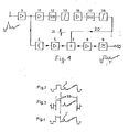
- the uncorrected video signal 1 passes from terminal 2 via amplifier 3, delay element 4 and amplifier 5 to adder 7. From there the video signal passes through amplifier 8 and low pass 9 with a cutoff frequency of 3. 0 MHz to the output terminal 10 at which the corrected video signal 1 'is available.
- the video signal 1 From the output of the amplifier 3, the video signal 1 also reaches the differentiating stage 12 via the amplifier 11.
- the amplitude limiter 13 is located at the output of the differentiating stage 12 and limits the signal amplitudes of the differentiated signal in positive and negative directions.
- the signal differentiated in this way and limited in amplitude reaches the second differentiating stage 17 via the amplifier 16.
- This is also followed by a limiter 18, which acts like the limiter 13.
- the amplitude of the correction signal 21 and the limiter values of the limiters 13, 18 are selected such that the amplitude limiters 13, 18 are practically ineffective in the case of small signal jumps in the video signal 1, the correction signal 21 is not limited and a desired steepening of the edges in the video signal occurs that but with larger signal jumps in the video signal 1 in the corrected video signal 1 'there are no excessive voltage peaks which can disturb the image reproduction or the synchronization.
- FIG. 2 shows the uncorrected video signal 1 at the terminal 2.
- the video signal contains a relatively wide black / white jump, a so-called 20T pulse and five small signal jumps. These small signal jumps are particularly distributed by the circuit.
- FIG. 3 shows a corrected video signal as it would be in a known manner with a circuit according to FIG. 1 without the limiter at terminal 10.
- the five small signal jumps experience a desired steepening, which brings about a subjectively better image reproduction.
- extremely high voltage peaks 33 occur, which reach three times the value of the signal jumps contained in the video signal.
- These extremely high signal jumps lead to a subjective image deterioration. Since they exceed the synchronous floor of the line synchronizing pulses, they can also interfere with the line deflection circuit, which operates in an amplitude-dependent manner, during image reproduction.
- FIG. 4 shows the corrected video signal 1 ′ at the terminal 10, which occurs when the limiters 13, 18 in FIG. 1 are used.
- the five small signal jumps experience approximately the same steepening as in FIG. 3, because the limiters 13, 18 remain ineffective with these amplitude jumps.
- the undesirable large voltage peaks 33 according to FIG. 3 are, however, greatly reduced by the limiters 13, 18.
- germanium diodes When switched on, the germanium diode has a lower resistance than a silicon diode, but has a dynamic internal resistance in the pass band, which becomes undesirably larger with large currents.
- silicon diode is not as low-resistance as a germanium diode, it also maintains approximately a constant dynamic internal resistance within the passband even with large signal currents.
- the advantages of the two different types of diodes are now advantageously combined in the invention. This combination results in an overall particularly low internal resistance in the switched-through area, which is effective both with small and with larger signal currents. This measure significantly improves the switching properties of the diodes at the threshold value given by the forward voltage and thus the effect of the limiter.
- diodes with the desired properties are not always available in sufficient numbers. It is then necessary to select diodes with certain properties from a large quantity for the circuit to function properly. However, such a solution is unsuitable for series production. If the diodes do not have the desired properties, the desired switching behavior of the diodes for amplitude limitation is not optimal.
- the necessary limitation is therefore realized without diodes, in that the diodes are formed by the collector-emitter paths of two transistors of the same type which are polarized in opposite directions, the collectors of which are each connected to the base.
- transistors as diodes for the limitation, an increased variety of semiconductor components is available.
- the transistors can be switched in a manner known per se so that they perform the function of a diode.
- a transistor connected as a diode in the. Passband is lower resistance than a diode.
- the forward resistance of the transistor operating as a diode can be influenced, for example intentionally increased, by a special switching of the transistor according to a development of the invention. This can be useful in order to avoid the entire circuit due to a low-impedance controlled Transi Stor undesirably heavy and dampen.
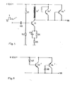
- the video signal 1 is fed to the transistor 11 via the capacitor 60, the base bias of which is determined by the voltage divider 61, 62.
- the emitter of the transistor 11 is grounded via the RC element with the capacitor 63 and the resistor 64 and via the resistor 65.
- the once differentiated correction signal is present at terminal 66 and is fed to a further differentiation stage according to FIG.
- the differentiation takes place with the inductance 12 'in the collector circuit of the transistor 11.
- the two silicon transistors 13 ', 14' are connected antiparallel, the collector being connected to the base.
- the transistors 13 ', 14' act in this circuit like two anti-parallel diodes.
- the forward resistance of the transistors 13 ', 14' is intentionally increased by connecting the collector to the base via a diode 67, 68.
- the diodes 67, 68 make the switching behavior of the transistors 13 ', 14' softer and the forward resistance increased in a desired manner. As a result, a lower load and damping of the amplifier with the transistor 11 can be achieved.
- germanium diodes 67, 68 are preferably used because they have a lower forward resistance at small signal amperages than silicon diodes.
- the dynamic internal resistance of the germanium diodes increases with large signal amplitudes, while it remains almost constant with silicon diodes. The pairing of the germanium diodes 67, 68 and the silicon transistors 13 ', 14' to maintain a switch-like limiter with a defined internal resistance is therefore advantageous.
- the video signal is recorded in a video recorder in the form of a carrier frequency-modulated with the video signal. Due to the frequency response of the recording head and the magnetic tape, the entire transmission characteristic has a drop towards high frequencies. Statistically speaking, high-frequency signal components in particular have a relatively small amplitude. To improve the reproduction of fine picture details, it is therefore known to guide the video signal in front of the FM modulator via a so-called pre-emphasis, in which the high frequencies are raised. During playback, the high frequencies are reduced accordingly in a de-emphasis circuit. This also improves the signal-to-noise ratio for these high frequency components. If the circuit according to FIG.
- the signal falsification caused by the pre-emphasis is avoided with simple circuit means. This is achieved in that an amplifier located in the recording path of the recorder in front of a frequency modulator and used for preemphasis of the video signal is provided with a negative feedback network with negative feedback increasing towards high frequencies.
- the known pre-emphasis circuit has a gain that increases continuously with increasing frequency. This is advantageous for a video signal not processed according to FIG. 1 in the sense of a perfect signal transmission.
- the gain which is effective in the pre-emphasis circuit and increases towards high frequencies is disadvantageous because the signal jumps containing high frequencies are then overemphasized.
- This disadvantage is eliminated by the fact that the pre-emphasis circuit has a defined negative feedback that increases towards high frequencies. This advantageously counteracts the increase in amplification to high frequencies present in the pre-emphasis circuit.
- the pre-emphasis circuit therefore has two frequency-dependent networks which act independently of one another. One is still used in the sense of preemphasis to increase the gain towards high frequencies. The other serves to reduce the gain in a defined frequency range.
- FIG. 7 shows the video image corresponding to FIG. 1 Signal 1 at terminal 2, amplifier 3, delay element 4, amplifier 5, adder 7, amplifier 8, low pass 9 and terminal 10, at which the video signal 1 processed according to the invention in the sense of increasing the sharpness of the image 'stands.
- the correction signal 21 is added to the video signal. This is obtained in the way with the amplifier 11, the differentiating stage 12, the amplitude limiter 13, the second amplifier 16, the second differentiating stage 17 and the second amplitude limiter 18 from the video signal 1.
- the video signal 1 ' is fed to the pre-emphasis circuit 32 via the line 30 and the capacitor 31. At its output, the latter supplies the video signal via capacitor 33 to FM modulator 34. The latter produces a carrier which is frequency-modulated with the video signal and which is recorded with head 35 on magnetic tape 36.
- the circuit 32 contains, in a known manner, the resistors 37, 38 used to generate the base bias, the transistor 39 with the collector load resistor 40, the emitter resistor 41 and the frequency-dependent negative feedback network with the resistors 42, 43 and the capacitors 44, 45.
- the signal from the output of the transistor 39 passes through the emitter follower stage with the transistor 46 and the load resistor 47 to the output of the circuit 32.
- the network 42-45 causes negative feedback that decreases towards high frequencies and thus increases the amplification of the video signal 1 'for preemphasis.
- the circuit 32 additionally contains the negative feedback network with the resistor 48 and the capacitor 49. This network causes negative feedback increasing towards high frequencies and thus a decreasing gain of the transistor 39.
- the time constant of the network 48, 49 is in the order of 200 ns, which corresponds to a cut-off frequency of approximately 0.9 M Hz.
- FIG. 8a shows the pulse shape of a rectangular pulse, which according to a known pre-emphasis circuit, ie without the network 48, 49 and without processing the video signal
- Figure 1 arises from an input pulse according to Figure 2b.
- This pulse has the form necessary for recording with frequency modulation.
- a pulse according to FIG. 8 c would arise at the output of the pre-emphasis circuit.
- the voltage peaks shown are higher than shown as a result of the effect of the increase at high frequencies. They are limited in amplitude by the operating voltage.
- the undesired curve deformation from FIG. 8a to FIG. 8c occurs regardless of the change in amplitude.
- a distorted pulse according to FIG. 8d would result during playback.
- a pulse according to FIG. 8e is generated at the output of the circuit 32.
- This pulse has approximately the same amplitude as the pulse according to FIG. 8c, but again the correct curve shape according to FIG. 8a.
- This overemphasis results in an image improvement in the form of a sharper display of fine image details at high frequencies.
- the circuit 32 is fed from the terminal 10 to its input with a processed video signal 1 'with a peak-to-peak amplitude of approximately 1 V.
- the pre-emphasis and the frequency-dependent negative feedback introduced to reduce the high-frequency pulse peaks take place in the same amplifier stage with the transistor 39. This is not absolutely necessary.
- the pre-emphasis and the negative feedback mentioned can also be in separate stages which follow one another in the signal path.
- the components in the circuit 32 had the following values.
- the following interference can occur. If the receiver is not optimally tuned, the reproduced image can be replaced by an image plastic when using the circuit. and noise are affected. Under certain conditions, the image reproduction can then be subjectively worse than without using the circuit according to the invention.
- FIGS. 9 and 10 show a development of the invention, by means of which disturbances occurring in the case of non-optimal coordination are avoided by the amplitude. of the correction signal is reduced with increasing amplitude of the signal components in the upper frequency range of the uncorrected video signal.
- the correction voltage can be reduced continuously as the amplitude of the high frequency signal components in the video signal increases.
- Another embodiment consists in completely switching off the correction signal when the signal components of higher frequency in the video signal exceed a certain threshold value.
- the circuit according to FIG. 1 is ineffective and thus does not contribute to image improvement.
- the circuit of FIG. 1 is prevented from undesirably affecting the image quality in the event of a mismatch.
- the gate 70 is additionally inserted, which is permeable when the television receiver is optimally matched.
- the video signal from the output of the amplifier 5 reaches the filter 71, which has a pass band at about 2-3 MHz. If the receiver is incorrectly tuned, the signal components in this frequency range are greatly increased, so that an excessive voltage occurs at the output of the filter 71. This voltage is rectified in the rectifier 72. If the rectified voltage exceeds a certain threshold value, the switching voltage 73 arises in a threshold value circuit, not shown. This switching voltage controls the gate 70 impermeably, so that the correction voltage 21 no longer reaches the adder 7. The correction circuit 11-13, 16-18 is then ineffective in the desired manner. When the receiver is properly tuned again, the amplitude of the signal components in the upper frequency range of the video signal at the output of the amplifier 5 drops again. The switching voltage 73 then disappears and the gate 70 is again controlled to be permeable. The correction voltage 21 then reaches the adding stage 7 again in the desired manner.
- the video signal passes from the output of the amplifier 5 via the capacitor 74 to the base of the transistor 75, the base bias of which is generated by the voltage divider 76, 77 and the emitter is grounded via the resistor 78.
- the filter 71 tuned to 2-3 MHz, which is damped by the resistor 79.
- the collector is connected to the base of transistor 16a, which represents amplifier 16 in FIG.
- the base bias for transistor 16a is generated with resistors 83, 84.
- the emitter of transistor 16a is grounded through resistor 85 and capacitor 86.
- the differentiating stage is formed by the inductance 17a and the amplitude limiter 18 by two anti-parallel diodes 18a.
- the video signal passes from the limiter 13 through the capacitor 87 to the base of the transistor 16a.
- the signal components produced at the filter 71 and the direct voltage obtained therefrom at the base of the transistor 81 are so small that the transistor 81 remains blocked and has no influence on the function of the transistor 16a.
- the correction voltage 21 then reaches the input of the adder 7 in order to increase the sharpness.
- the tuning is not optimal, the DC voltage at the base of transistor 81 becomes so great that transistor 81 conducts and grounds the base of transistor 16a. As a result, the correction voltage 21 at the input of the adder 7 disappears.
- the transistor 81 thus acts as an amplitude threshold circuit and the transistor 16a as a gate 70 in FIG. 9.
- the low pass 9 preferably has the cut-off frequency of 3.5 MHz in a color television receiver.
- a low-pass filter with the same cut-off frequency is preferably provided in series with amplifier 3.
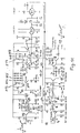
- FIG. 11 shows a circuit that has been tried and tested in accordance with the block diagram according to FIG. 1, parts which correspond to one another are provided with the same reference numbers.
- the transistor 30 In the path of the video signal 1 are the transistor 30, the low pass 31 with a cutoff frequency of 3.0 M Hz, the transistor 32 and the transistor 23 operated as an emitter follower.
- the circuit point 6 at the base of the transistor 27 is the point at which the Video signal and the correction signal 21 are added.
- the coil 212 in the collector circuit of the transistor 211 acts as a differentiator. Silicon diodes 213, 214 connected in anti-parallel are parallel to the coil 212.
- the diodes 213, 214 have a limiting effect at a voltage of approximately 0.2 volts.
- the transistor 216 forms the second amplifier stage and the coil 217 the second differentiator.
- the diodes 218, 219 again effect the amplitude limitation.
- the correction signal passes from the collector of transistor 216 to circuit 15, which only allows signals above a certain threshold value and thereby suppresses noise below this threshold value.
- the correction signal at the output of the circuit 15 then reaches the two limiters 90, 91, which additionally limit the correction signal in the positive and negative directions, so that the correction signal 21 at the circuit point 6 has the optimal maximum amplitude relative to the video signal 1.
Claims (10)
Priority Applications (1)
| Application Number | Priority Date | Filing Date | Title |
|---|---|---|---|
| AT82109220T ATE18619T1 (de) | 1981-10-14 | 1982-10-06 | Schaltung zur versteilerung der flanken eines videosignals, insbesondere fuer einen videorecorder. |
Applications Claiming Priority (4)
| Application Number | Priority Date | Filing Date | Title |
|---|---|---|---|
| DE3140761 | 1981-10-14 | ||
| DE19813140761 DE3140761C2 (de) | 1981-10-14 | 1981-10-14 | Schaltung zur Versteilerung der Flanken eines Videosignals, insbesondere für einen Videorecorder |
| DE3206685 | 1982-02-25 | ||
| DE3206685 | 1982-02-25 |
Publications (2)
| Publication Number | Publication Date |
|---|---|
| EP0077010A1 EP0077010A1 (fr) | 1983-04-20 |
| EP0077010B1 true EP0077010B1 (fr) | 1986-03-12 |
Family
ID=25796691
Family Applications (1)
| Application Number | Title | Priority Date | Filing Date |
|---|---|---|---|
| EP82109220A Expired EP0077010B1 (fr) | 1981-10-14 | 1982-10-06 | Circuit pour réduire le temps de montée des flancs d'un signal vidéo, notamment pour enregistreur vidéo |
Country Status (2)
| Country | Link |
|---|---|
| EP (1) | EP0077010B1 (fr) |
| DE (1) | DE3269852D1 (fr) |
Families Citing this family (9)
| Publication number | Priority date | Publication date | Assignee | Title |
|---|---|---|---|---|
| DE3307014A1 (de) * | 1983-02-28 | 1984-08-30 | Telefunken Fernseh Und Rundfunk Gmbh, 3000 Hannover | Schaltung zur verbesserung der bildschaerfe bei einem videorecorder |
| JPS59186493A (ja) * | 1983-04-07 | 1984-10-23 | Victor Co Of Japan Ltd | カラ−映像信号処理装置 |
| DE3400674C1 (de) * | 1984-01-11 | 1985-03-21 | Deutsche Thomson-Brandt Gmbh, 7730 Villingen-Schwenningen | Schaltung zur Versteilerung der Flanken eines Videosignals |
| US4706113A (en) * | 1985-02-18 | 1987-11-10 | Mitsubishi Denki Kabushiki Kaisha | Contour detecting filter device using PAL samples of composite video signals without separation of luminance signals therefrom |
| DE3713225C1 (de) * | 1987-04-18 | 1988-08-11 | Standard Elektrik Lorenz Ag | Videogeraet mit einem Aufzeichnungstraeger |
| US4935806A (en) * | 1988-12-30 | 1990-06-19 | Zenith Electronics Corporation | Chroma noise reduction and transient improvement |
| DE3940128A1 (de) * | 1989-04-27 | 1990-10-31 | Thomson Brandt Gmbh | Schaltung zur aufbereitung eines leuchtdichtesignals |
| KR920010186B1 (ko) * | 1990-10-30 | 1992-11-19 | 주식회사 금성사 | 비디오 카세트 레코더의 화상제어시스템 |
| GB2253964A (en) * | 1991-03-20 | 1992-09-23 | Rank Cintel Ltd | Treatment of video signals produced by aperture correctors |
Family Cites Families (6)
| Publication number | Priority date | Publication date | Assignee | Title |
|---|---|---|---|---|
| DE1512688A1 (de) * | 1967-01-18 | 1969-06-12 | Fernseh Gmbh | Schaltungsanordnung zur zweiseitigen Amplitudenbegrenzung elektrischer Signale |
| JPS5286010A (en) * | 1976-01-12 | 1977-07-16 | Sony Corp | Pre-emphasis circuit |
| GB1579138A (en) * | 1976-07-06 | 1980-11-12 | Sony Corp | Noise and cross-talk elimination in recording and reproducing video signals |
| JPS5327010A (en) * | 1976-08-25 | 1978-03-13 | Sony Corp | Signal tran smitter |
| JPS5412714A (en) * | 1977-06-29 | 1979-01-30 | Matsushita Electric Ind Co Ltd | Recorder-reproducer |
| JPS55117712A (en) * | 1979-02-28 | 1980-09-10 | Matsushita Electric Ind Co Ltd | Noise reduction circuit of video signal recording and reproducing device |
-
1982
- 1982-10-06 EP EP82109220A patent/EP0077010B1/fr not_active Expired
- 1982-10-06 DE DE8282109220T patent/DE3269852D1/de not_active Expired
Also Published As
| Publication number | Publication date |
|---|---|
| DE3269852D1 (en) | 1986-04-17 |
| EP0077010A1 (fr) | 1983-04-20 |
Similar Documents
| Publication | Publication Date | Title |
|---|---|---|
| DE3430933C2 (fr) | ||
| DE2828586C2 (de) | Aufzeichnungs- und Wiedergabesystem für Videosignale | |
| DE1908247A1 (de) | Schaltungsanordnung zur Verringerung von Stoerungen hoeherer Frequenz (Rauschen) in breitbandigen elektrischen Signalen,insbesondere Fernsehsignalen | |
| DE2733350C2 (de) | Schaltungsanordnung zur Beseitigung von Amplitudenschwankungen bei der Wiedergabe eines auf einem Aufzeichnungsträger aufgezeichneten Signals | |
| DE3315663C2 (de) | Schaltung zur dynamischen Unterdrückung kleiner Wechselsignalamplituden für ein Bildwiedergabesystem | |
| EP0077010B1 (fr) | Circuit pour réduire le temps de montée des flancs d'un signal vidéo, notamment pour enregistreur vidéo | |
| DE2730131C2 (fr) | ||
| EP0098015B1 (fr) | Arrangement de circuit pour augmenter la netteté de contours d'un signal vidéo | |
| DE2822837A1 (de) | Anordnung zur verminderung des stoeranteils in nutzsignalen | |
| DE3237421A1 (de) | Anordnung zur automatischen und manuellen regelung der versteilerung in videosignalen | |
| DE2547143A1 (de) | Schaltungsanordnung zur automatischen bandbreitenregelung eines leuchtdichtekanals | |
| DE3214607C2 (fr) | ||
| DE2613071B2 (de) | Einrichtung zur unterdrueckung von einschwing-stoerspitzen in fernsehsignalen | |
| DE3011726C2 (de) | Stabilisierte automatische Helligkeitsregelschaltung in einem Videosignalverarbeitungssystem mit automatischem Strahlstormbegrenzer | |
| DE3234797C2 (de) | Anordnung zur Verarbeitung von Videosignalen | |
| DE3311883C2 (de) | Schaltung zur Versteilerung von Videosignalen | |
| DE3140761C2 (de) | Schaltung zur Versteilerung der Flanken eines Videosignals, insbesondere für einen Videorecorder | |
| DE3516913C1 (de) | Automatische FM-Seitenband-Pegelregelung fuer Video-Recorder | |
| DE1951295B2 (de) | Regelbarer transistorverstaerker | |
| DE3030313C2 (de) | Schaltung zur Unterdrückung hochfrequenter Störungen in einem Fernsehempfänger | |
| DE2919164C3 (de) | Videosignalentzerrungsschaltung | |
| DE3237422C2 (de) | Frequenzselektive Signalverarbeitungsschaltung | |
| DE3400674C1 (de) | Schaltung zur Versteilerung der Flanken eines Videosignals | |
| DE3725683C2 (de) | Aufzeichnungsgerät für Videosignale | |
| DE2854828C2 (fr) |
Legal Events
| Date | Code | Title | Description |
|---|---|---|---|
| PUAI | Public reference made under article 153(3) epc to a published international application that has entered the european phase |
Free format text: ORIGINAL CODE: 0009012 |
|
| AK | Designated contracting states |
Designated state(s): AT BE CH DE FR GB IT LI LU NL SE |
|
| 17P | Request for examination filed |
Effective date: 19830824 |
|
| ITF | It: translation for a ep patent filed |
Owner name: BARZANO' E ZANARDO MILANO S.P.A. |
|
| GRAA | (expected) grant |
Free format text: ORIGINAL CODE: 0009210 |
|
| RAP1 | Party data changed (applicant data changed or rights of an application transferred) |
Owner name: TELEFUNKEN FERNSEH UND RUNDFUNK GMBH |
|
| AK | Designated contracting states |
Kind code of ref document: B1 Designated state(s): AT BE CH DE FR GB IT LI LU NL SE |
|
| REF | Corresponds to: |
Ref document number: 18619 Country of ref document: AT Date of ref document: 19860315 Kind code of ref document: T |
|
| REF | Corresponds to: |
Ref document number: 3269852 Country of ref document: DE Date of ref document: 19860417 |
|
| ET | Fr: translation filed | ||
| PLBI | Opposition filed |
Free format text: ORIGINAL CODE: 0009260 |
|
| 26 | Opposition filed |
Opponent name: GRUNDIG E.M.V. ELEKTRO-MECHANISCHE VERSUCHSANSTALT Effective date: 19861210 |
|
| NLR1 | Nl: opposition has been filed with the epo |
Opponent name: GRUNDIG E.M.V. MAX GRUNDIG HOLLAEND STIFTUNG & CO. |
|
| PGFP | Annual fee paid to national office [announced via postgrant information from national office to epo] |
Ref country code: SE Payment date: 19901018 Year of fee payment: 9 |
|
| PGFP | Annual fee paid to national office [announced via postgrant information from national office to epo] |
Ref country code: GB Payment date: 19910731 Year of fee payment: 10 |
|
| PGFP | Annual fee paid to national office [announced via postgrant information from national office to epo] |
Ref country code: AT Payment date: 19911010 Year of fee payment: 10 |
|
| PGFP | Annual fee paid to national office [announced via postgrant information from national office to epo] |
Ref country code: FR Payment date: 19911017 Year of fee payment: 10 |
|
| ITTA | It: last paid annual fee | ||
| PGFP | Annual fee paid to national office [announced via postgrant information from national office to epo] |
Ref country code: NL Payment date: 19911031 Year of fee payment: 10 Ref country code: CH Payment date: 19911031 Year of fee payment: 10 |
|
| PGFP | Annual fee paid to national office [announced via postgrant information from national office to epo] |
Ref country code: DE Payment date: 19911224 Year of fee payment: 10 |
|
| RDAG | Patent revoked |
Free format text: ORIGINAL CODE: 0009271 |
|
| STAA | Information on the status of an ep patent application or granted ep patent |
Free format text: STATUS: PATENT REVOKED |
|
| 27W | Patent revoked |
Effective date: 19911128 |
|
| GBPR | Gb: patent revoked under art. 102 of the ep convention designating the uk as contracting state | ||
| REG | Reference to a national code |
Ref country code: CH Ref legal event code: PL |
|
| NLR2 | Nl: decision of opposition | ||
| PGFP | Annual fee paid to national office [announced via postgrant information from national office to epo] |
Ref country code: LU Payment date: 19920924 Year of fee payment: 11 |
|
| PGFP | Annual fee paid to national office [announced via postgrant information from national office to epo] |
Ref country code: BE Payment date: 19921028 Year of fee payment: 11 |
|
| EPTA | Lu: last paid annual fee | ||
| EUG | Se: european patent has lapsed |
Ref document number: 82109220.2 Effective date: 19920311 |
|
| APAH | Appeal reference modified |
Free format text: ORIGINAL CODE: EPIDOSCREFNO |