EP0075367B1 - Infra-red radiation imaging devices - Google Patents
Infra-red radiation imaging devices Download PDFInfo
- Publication number
- EP0075367B1 EP0075367B1 EP82201146A EP82201146A EP0075367B1 EP 0075367 B1 EP0075367 B1 EP 0075367B1 EP 82201146 A EP82201146 A EP 82201146A EP 82201146 A EP82201146 A EP 82201146A EP 0075367 B1 EP0075367 B1 EP 0075367B1
- Authority
- EP
- European Patent Office
- Prior art keywords
- radiation
- charge
- superlattice structure
- semiconductor layer
- carriers
- Prior art date
- Legal status (The legal status is an assumption and is not a legal conclusion. Google has not performed a legal analysis and makes no representation as to the accuracy of the status listed.)
- Expired
Links
- 230000005855 radiation Effects 0.000 title claims description 92
- 238000003384 imaging method Methods 0.000 title claims description 21
- 239000004065 semiconductor Substances 0.000 claims description 40
- 238000012545 processing Methods 0.000 claims description 33
- 239000002800 charge carrier Substances 0.000 claims description 26
- 239000000758 substrate Substances 0.000 claims description 18
- 229910052710 silicon Inorganic materials 0.000 claims description 16
- 239000010703 silicon Substances 0.000 claims description 16
- 239000000463 material Substances 0.000 claims description 13
- 230000015556 catabolic process Effects 0.000 claims description 11
- 238000012546 transfer Methods 0.000 claims description 9
- 238000010521 absorption reaction Methods 0.000 claims description 7
- 230000005284 excitation Effects 0.000 claims description 5
- 230000004888 barrier function Effects 0.000 claims description 4
- 238000005452 bending Methods 0.000 claims description 4
- 230000000779 depleting effect Effects 0.000 claims description 3
- 230000005684 electric field Effects 0.000 claims description 3
- 230000007704 transition Effects 0.000 claims description 3
- 238000001514 detection method Methods 0.000 claims 1
- XUIMIQQOPSSXEZ-UHFFFAOYSA-N Silicon Chemical compound [Si] XUIMIQQOPSSXEZ-UHFFFAOYSA-N 0.000 description 15
- 230000008901 benefit Effects 0.000 description 4
- 239000000969 carrier Substances 0.000 description 3
- 230000009471 action Effects 0.000 description 2
- 239000012535 impurity Substances 0.000 description 2
- 229910052751 metal Inorganic materials 0.000 description 2
- 239000002184 metal Substances 0.000 description 2
- 238000000034 method Methods 0.000 description 2
- 238000005036 potential barrier Methods 0.000 description 2
- GYHNNYVSQQEPJS-UHFFFAOYSA-N Gallium Chemical compound [Ga] GYHNNYVSQQEPJS-UHFFFAOYSA-N 0.000 description 1
- NINIDFKCEFEMDL-UHFFFAOYSA-N Sulfur Chemical compound [S] NINIDFKCEFEMDL-UHFFFAOYSA-N 0.000 description 1
- 239000005864 Sulphur Substances 0.000 description 1
- 230000002411 adverse Effects 0.000 description 1
- 238000000137 annealing Methods 0.000 description 1
- 230000015572 biosynthetic process Effects 0.000 description 1
- 230000008859 change Effects 0.000 description 1
- 238000001816 cooling Methods 0.000 description 1
- 230000001186 cumulative effect Effects 0.000 description 1
- 230000007547 defect Effects 0.000 description 1
- 238000005137 deposition process Methods 0.000 description 1
- 238000011161 development Methods 0.000 description 1
- 238000010586 diagram Methods 0.000 description 1
- 238000005516 engineering process Methods 0.000 description 1
- 229910052733 gallium Inorganic materials 0.000 description 1
- 229910052738 indium Inorganic materials 0.000 description 1
- APFVFJFRJDLVQX-UHFFFAOYSA-N indium atom Chemical compound [In] APFVFJFRJDLVQX-UHFFFAOYSA-N 0.000 description 1
- 230000010354 integration Effects 0.000 description 1
- 230000002452 interceptive effect Effects 0.000 description 1
- 238000005468 ion implantation Methods 0.000 description 1
- 238000002955 isolation Methods 0.000 description 1
- 238000012986 modification Methods 0.000 description 1
- 230000004048 modification Effects 0.000 description 1
- 229910021421 monocrystalline silicon Inorganic materials 0.000 description 1
- 230000003287 optical effect Effects 0.000 description 1
- 230000003647 oxidation Effects 0.000 description 1
- 238000007254 oxidation reaction Methods 0.000 description 1
- 230000000737 periodic effect Effects 0.000 description 1
- 238000011160 research Methods 0.000 description 1
- 239000003362 semiconductor superlattice Substances 0.000 description 1
- 229910021332 silicide Inorganic materials 0.000 description 1
- 239000002210 silicon-based material Substances 0.000 description 1
- 239000007787 solid Substances 0.000 description 1
- 229910052716 thallium Inorganic materials 0.000 description 1
- BKVIYDNLLOSFOA-UHFFFAOYSA-N thallium Chemical compound [Tl] BKVIYDNLLOSFOA-UHFFFAOYSA-N 0.000 description 1
Images

Classifications
-
- H—ELECTRICITY
- H10—SEMICONDUCTOR DEVICES; ELECTRIC SOLID-STATE DEVICES NOT OTHERWISE PROVIDED FOR
- H10F—INORGANIC SEMICONDUCTOR DEVICES SENSITIVE TO INFRARED RADIATION, LIGHT, ELECTROMAGNETIC RADIATION OF SHORTER WAVELENGTH OR CORPUSCULAR RADIATION
- H10F39/00—Integrated devices, or assemblies of multiple devices, comprising at least one element covered by group H10F30/00, e.g. radiation detectors comprising photodiode arrays
- H10F39/10—Integrated devices
- H10F39/12—Image sensors
- H10F39/15—Charge-coupled device [CCD] image sensors
- H10F39/157—CCD or CID infrared image sensors
Definitions
- This invention relates to infra-red radiation imaging devices comprising a charge-transfer shift register, particularly but not exclusively a silicon charge-coupled device.
- U.K. Patent Specification GB-A-1,564,107 describes an infra-red radiation imaging device comprising a semiconductor body having a radiation-sensitive portion in which charge-carriers are generated on absorption of infra-red radiation incident on the device and a signal-processing portion having a charge-transfer shift register in which the radiation-generated charge-carriers are collected and are transported to an output from which an electrical signal representative of the detected radiation is derived.
- the semiconductor material of the signal-processing portion has an energy band gap which is greater than the quantum energy of the detected infra-red radiation. Means are present for depleting at least the radiation-sensitive portion of free charge-carriers in the absence of said radiation.
- Said radiation-sensitive portion is of the same semiconductor material as said signal-processing portion.
- the imaging devices described in GB-A--1,564,107 are charge-coupled devices, and advantages are obtained by using a common silicon body for both the CCD signal-processing portion and the radiation-sensitive portion. Both the radiation-sensitive portion and the signal-processing portion have an energy band gap which is greater than the quantum energy of the detected infra-red radiation.
- the radiation-sensitive portion is formed by providing at least a portion of the silicon body with a concentration of at least one deep-level impurity which provides centres for trapping majority charge-carriers which can be released upon excitation by infra-red radiation in a given wavelength range. Therefore the quantum efficiency of the device is dependant on the number of majority carriers trapped on deep-level centres, and the body must be cooled to low temperatures to prevent significant thermal excitation of the centres.
- the radiation-sensitive portion In order to obtain a high detectivity with this known device having deep-level centres, a very large number of said centres are desired in the radiation-sensitive portion, for example up to lo l6 per cm 2 .
- the centres may be formed by doping the body portion with for example indium, thallium, gallium or sulphur, or by introducing defect levels by radiation damage of the silicon lattice, for example using proton bombardment.
- high concentrations of centres may be difficult to achieve in a thin layer, for example because of solid solubility limitations, and such high concentrations may be difficult to incorporate without interfering with characteristics of the signal-processing portion, for example the CCD charge transfer characteristics.
- the radiation-sensitive portion can be depleted of free charge-carriers while avoiding breakdown only as a result of substantially all of the deep-level centres within the depletion region being full of majority charge-carriers. If the charge state of a substantial fraction of the deep-level centres is changed in the depletion regions then breakdown would occur so that this limits the intergra- tion period for the device, i.e. the period in which the maximum radiation can be incident on a particular imaging elemental portion of the device before it becomes necessary to replenish the centres with majority carriers by refreshing. In practice with a silicon device this can limit the number of centres which may change charge state to, for example, not more than 10 12 per cm 2 in said integration period.
- an infra-red radiation imaging device comprising a semiconductor body having a radiation-sensitive portion in which charge-carriers are generated on absorption of infra-red radiation incident on the device and a signal-processing portion having a charge-transfer shift-register in which the radiation-generated charge-carriers are collected and are transported to an output from which an electrical signal representative of the detected radiation is derived, the semiconductor material of the signal-processing portion having an energy band gap which is greater than the quantum energy of the detected infra-red radiation, and means for depleting at least the radiation-sensitive portion of free charge-carriers in the absence of said radiation, said radiation-sensitive portion being of the same semiconductor material as said signal-processing portion, is characterized in that said radiation-sensitive portion comprises a plurality of alternating n-type and p-type layers which form an energy band bending superlattice structure locally in the body with a reduced effective band gap, the n-type and p-type layers have a doping concentration and thickness such that
- Such an imaging device in accordance with the invention retains advantages of forming the radiation-sensitive and signal-processing portions in a common semiconductor body of the same semiconductor material, for example silicon, while avoiding disadvantages of using a high concentration of deep-level centres for the radiation-sensitive portion.
- a high quantum efficiency and high detectivity can be obtained, and in general less cooling of the device (to prevent significant thermal generation of carriers by such transis- tions) will be necessary.
- the radiation-sensitive portion can be very thin (e.g. less than 0.5 micrometre for the total thickness of the superlattice structure) so that cross-talk between detecting elements of the imaging device can be reduced.
- the reduced effective bandgap in the radiation-sensitive portion of the body can result from the Brillouin zone associated with the actual semiconductor lattice of the body material being divided into smaller zones (so-called "mini-zones") which are formed in momentum space (wave vector space) by the spatially alternating potential variation associated with the alternating conductivity- type layer structure of the radiation-sensitive portion.
- mini-zones are formed in momentum space (wave vector space) by the spatially alternating potential variation associated with the alternating conductivity- type layer structure of the radiation-sensitive portion.
- the formation of a superlattice structure by such division of the Brillouin zone is described in United States Patents US-A-3626257 and US-A-3626328, and in the article entitled “Superlattice and Negative Differential Conductivity in Semiconductors" by L. Esaki et al. in IBM Journal Research Development No. 14, January 1970, pages 61 to 65.
- the effective band gap can also be reduced by band-gap tunnelling of the charge-carriers
- Infared detectors having a semiconductor superlattice structure are known from the article of Esaki ; et al in IBM Technical Disclosure Bulletin Vol. 22 No. 3(1979.08) pages 1262-1264.
- the signal-processing portion may comprise a semiconductor layer of one conductivity type which extends above the radiation-sensitive portion formed by the superlattice structure
- the charge-transfer shift-register may comprise electrode means present on the semiconductor layer for capacitively producing electric fields in the semiconductor layer by means of which charge-carriers generated in the superlattice structure by the infra-red radiation can be introduced into said semiconductor layer of the one conductivity type and transported to the output to provide said electrical signal.
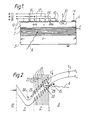
- the infra-red radiation imaging device of Figures 1 and 2 comprises a monocrystalline silicon semiconductor body 1 having a radiation-sensitive portion 2 and a signal-processing portion 3.
- Infra-red radiation 4 in a given wavelength range is imaged onto the device and penetrates to the radiation-sensitive portion 2 where absorption occurs generating free charge-carriers 24.
- the radiation-generated charge-carriers 24 are collected in the signal-processing portion 3 from which an electrical signal representative of the detected radiation image is derived at an output electrode 10.
- the signal processing portion of the device of Figures 1 and 2 is organized into a buried-channel charge-coupled device having CCD electrodes 11, 12 and 13.
- Both the body portions 2 and 3 are of silicon.
- the energy band gap Eg of silicon is approximately 1.1 eV which is greater than the quantum energy of the infra-red radiation which it is desired to detect.
- the quantum energy of radiation having a wavelength above 3 micrometres is at most approximately 0.4 eV, and a wavelength of, for example, 12 micrometres corresponds to a quantum energy of approximately 0.1 eV.
- the silicon body portion 2 is constructed in accordance with the present invention to have a reduced effective band gap so as to be sensitive to infra-red radiation having a quantum energy which is less than 1.1 eV.
- the radiation-sensitive portion 2 comprises a plurality of alternating n-type and p-type layers 21 and 22 (see Figure 2) which form an energy band bending superlattice structure locally in the body 1.
- the alternate layers 21 and 22 are sufficiently thin and highly-doped to introduce a spatially periodic potential variation over distances comparable with the electron wavelength in the semiconductor material, and this changes the electrical and optical properties of the material.
- an effective energy band gap Eg of less than 1.1 eV is obtained between the valence and conduction band edges Ev and E o even though the body portion 2 is of silicon. This is illustrated schematically in Figure 2.
- each n-type and p-type layer 21 and 22 determines the effective band-gap Eg' and hence determines the maximum radiation wavelength which will produce electron-hole pairs by excitation across the effective band gap Eg' on absorption in the body portion 2. Such transitions between the conduction and valence bands are illustrated by the arrow 20 in Figure 2.
- each n-type layer 21 may have a doping concentration of about 10 20 donor atoms per cm 3 and a thickness of about 2 nm (20 A) and each p-type layer may have a doping concentration of about 10 20 acceptor atoms per cm 3 and a thickness of about 3 nm (30 A).
- the total number of layers 21 and 22 must be sufficient to provide the energy band bending superlattice structure and also to provide an adequately thick body portion 2 for the absorption of the radiation 4.
- the total number of layers 21 and 22 may be 40 to 50 so that the radiation-sensitive portion 2 having the reduced effective band-gap Eg' is approximately 0.1 micrometres (10 3 A) thick. This very small thickness of the portion 2 reduces cross-talk between the detecting elements.
- the total number of layers 21 and 22 may be 40 to 50 so that the radiation-sensitive portion 2 having the reduced effective band-gap Eg' is approximately 0.1 micrometres (10 3 A) thick. This very small thickness of the portion 2 reduces cross-talk between the detecting elements.
- not all these layers 21 and 22 are included in Figure 1.
- each layer 21 and 22 is such that the superlattice structure of the body portion 2 can be depleted throughout its thickness without breakdown occurring.
- the positive and negative charge-states of the depleted layers 21 and 22 respectively are balanced sufficiently across the whole superlattice structure so that any cumulative imbalance in charge across the whole depleted superlattice structure totals less than the critical charge level for avalanche breakdown.
- the signal-processing portion 3 is in the form of an island provided by a portion of an epitaxial semiconductor layer of one conductivity type (n-type in the example given in Figures 1 and 2) which extends above the radiation-sensitive portion 2.
- the energy band gap Eg of the silicon material of this layer is unmodified by its doping and so is approximately 1.1 eV.
- the radiation-sensitive portion 2 formed by the superlattice structure is present on a substrate 5.
- the substrate is a low-doped region of the silicon body 1, has an unmodified energy band gap Eg of approximately 1.1 eV and is of the opposite conductivity type (p-type in the example given in Figures 1 and 2 with a doping concentration of for example 10 15 acceptor atoms per cm 3 ).
- the superlattice structure can be formed on the substrate 5 using known molecular beam epitaxial techniques to permit good control of the individual thicknesses and doping concentrations of each thin layer 21, 22.
- the much thicker layer (which provides the portion 3) can be formed subsequently on the superlattice structure also using epitaxial techniques.
- the more highly doped n-type zone (n+) which is contacted by the output electrode 10 can be formed by ion implantation using either a low temperature or pulsed laser-beam for annealing.
- the signal-processing layer portion 3 is laterally isolated in the epitaxial layer by reverse-biasing a Schottky barrier between the n-type layer and a Schottky electrode 6 which extends on the layer surface around the periphery of the CCD island portion 3. Only a part of the portion 3 and isolation electrode 6 adjacent the output electrode 10 is shown in Figure 1.
- a reverse-bias voltage is applied between the opposite conductivity type substrate 5 and layer portion 3 so as to form a depletion layer which fully depletes the body portions 2 and 3 in the absence of incident radiation 4.
- the thickness and doping concentration of the layer portion 3 may be for example 2.5 micrometres and 2x 10 15 atoms per cm 3 so that when fully depleted its charge level is approximately 5 ⁇ 10 11 cm -2 which is below the critical charge level for avalanche breakdown.
- the depleted layer portion 3 provides the charge-transfer channel portion of a buried-channel charge-coupled device.
- Electrodes 11, 12 and 13 which are present on the layer 3 form a sequence of gates which are arranged for CCD operation in known manner.
- clocking voltages 0(1), 0(2), 0(3) to the CCD electrodes 11,12, 13 electric fields are capacitively produced in the layer portion 3 by means of which charge-carriers 24 generated in the superlattice structure 2 by the radiation 4 can be introduced into the layer portion 3 and can be transported in discrete-packets to charge-reading means at the electrode 10 to provide the output signal.
- the CCD electrode means are a sequence of three Schottky gates 11, 12 and 13 provided by metal or metal- silicide layers which form Schottky barriers with the surface of the silicon layer portion 3. In operation these Schottky barriers are reverse- biased.
- the electrode means can be formed using low temperature technology which will not adversely modify the doping distribution and thicknesses of the previously-formed underlying layers 21 and 22 of the superlattice structure.
- the CCD electrode means may be in the form of conductive semiconductor or metal layers which are separated from the underlying silicon layer portion 3 by an insulating dielectric layer so forming insulated gates.
- Such an insulating layer may be formed in known manner by a low temperature deposition process or plasma oxidation.
- a 3-phase CCD structure is illustrated in Figure 1, the signal-processing may be effected with other arrangements, for example a 2-phase or 4-phase CCD arrangement.
- the imaging device of Figures 1 and 2 may be operated at a temperature of for example 77°K or higher, depending on the radiation to be detected.
- the radiation 4 may be incident on the back surface of the substrate 5, having been imaged onto the device body 1 via any known appropriate infra-red lens system.
- the radiation 4 is absorbed in the radiation-sensitive superlattice portion 2 where it generates electron-hole pairs 24, 26. Because these electron-hole pairs are generated by transitions 20 between the conduction and valence bands, the quantum efficiency and detectivity of this device in accordance with the invention can be much higher than for the known deep-level impurity CCD imaging devices of GB-A--1564107 and is not limited by the doping concentrations in the radiation-sensitive portion 2.
- the radiation-generated electrons and holes 24 and 26 move in opposite directions.
- the holes 26 are drained to earth via the p-type substrate 5, while the electrons 24 drift to the potential minimum below the nearest appropriately-biased CCD electrode 12 where they collect to form a packet of charge which is subsequently transferred along the layer portion 3 by CCD action to give an output signal.
- both electrons and holes 24 and 26 generated inside the superlattice structure 2 by the radiation 4 must each cross a succession of alternate n-type and p-type layers in order to reach the buried-channel layer portion 3 and the substrate 5 respectively.
- the high doping concentrations and small thicknesses chosen for the individual layers 21 and 22 are important in this respect to permit tunnelling of the electrons and holes 24 and 26 through the potential barriers presented by the individual layers 21 and 22. Such tunnelling of the electrons and holes 24 and 26 is illustrated in Figure 2 by arrows 23 and 25.
- the slope of the band edges in the portion 2 of Figure 2 also illustrates the drift field which results from the reverse-biasing of the layer portion 3 with respect to the substrate 5 and which results in the electrons 24 moving towards the layer portion 3 and in the holes 26 moving towards the substrate 5.
- layers 21 and 22 having an individual thickness of 2 and 3 nm and an individual doping concentration of 10 20 per cm 3 efficient tunnelling of the electrons and holes 24 and 26 occurs, even at the bottom of the potential wells associated with the layers 21 and 22.
- the holes 26 have a higher effective mass than the electrodes 24, the n-type layers 21 are preferably slightly thinner than the p-type layers 22, for example 2 nm instead of 3 nm.
- Figures 1 and 2 relate to a buried-channel CCD imaging device.
- the present invention is also applicable to imaging devices having other forms of signal processing in the same semiconductor body as the superlattice radiation-sensitive portion 2.
- Figure 3 illustrates part of a surface-channel CCD imaging device in accordance with the present invention.
- the superlattice structure of body portion 2 corresponds to that of the previous embodiments, the doping concentrations and thicknesses of its layers 21 and 22 being chosen in accordance with the requirements for detecting radiation of a given wavelength, and for permitting tunnelling of charge-carriers across a succession of alternate layers 21 and 22 of opposite conductivity types.
- the superlattice structure can be depleted of free charge-carriers across its whole thickness without avalanche breakdown occurring.
- the signal-processing portion 3 consists of a p-type epitaxial layer, and the output electrode 10 contacts an opposite-conductivity type region (n+) provided in the p-type layer 3.
- the electrons 24 generated in the superlattice can be introduced into the surface-channel CCD by local punch-through of a depletion region to the underlying superlattice radiation-sensitive portion 2 at sites below the individual CCD electrodes 11, 12 and 13 in accordance with the teaching in U.K. Patent Specification GB-A-1532859.
- the doping concentrations of both the layer 3 and the superlattice layers 21 and 22 are such that the depletion regions can extend locally through the thickness of both the layer 3 and the superlattice structure 2 without breakdown occurring.
- the dotted line 31 in Figure 3 illustrates the extent of the depletion regions in the layer 3 with punch-through below the electrodes 12.
- all the electrodes 11, 12 and 13 are present on a dielectric layer 30 to form insulated gates of the CCD.
- the radiation 4 may be incident at the surface of the layer portion 3.
- the superlattice structure 2 of Figure 3 is present on a substrate comprising a low-doped p-type layer 51 on a high-doped base 52, both of silicon.
- This substrate 51, 52 provides an ohmic contact.
- the superlattice structure 2 With no incident radiation 4, the superlattice structure 2 has a high resistance and there is negligible current flow between the substrate 51, 52 and the punch-through deplection regions (below electrode 12 in Figure 3).
- the radiation 4 is incident, electron-hole pairs are generated in the superlattice structure 2 and an electron current flows towards the punch-through deplection regions, electrons being replenished by a current flow from the substrate 51, 52.
- the holes generated by the radiation 4 move towards the substrate 51, 52 and either recombine with electrons from the substrate 51, 52 or are collected by the substrate 51, 52.
- the signal-processing p-type layer 3 has an ohmic contact electrically connected to the n-type substrate 51, 52 to permit fast CCD action.
- the conductivity types of all the semiconductor regions may be reversed to provide an imaging device in which the radiation-generated holes are collected and processed to give an output signal.
- the superlattice radiation-sensitive portion 2 need not underlie the signal-processing body portion 3, but the superlattice radiation-sensitive portion 2 may be provided side-by-side in the silicon body 1 with the signal-processing portion 3.
- the charge-carriers introduced into the portion 3 from the portion 2 do not need to tunnel through the potential barriers in the superlattice structure but may merely flow along the length of the individual layers 21 and 22 to a storage site in the body portion 3 below a gating electrode.
Landscapes
- Solid State Image Pick-Up Elements (AREA)
- Light Receiving Elements (AREA)
- Transforming Light Signals Into Electric Signals (AREA)
Applications Claiming Priority (2)
| Application Number | Priority Date | Filing Date | Title |
|---|---|---|---|
| GB8128310 | 1981-09-18 | ||
| GB08128310A GB2106314A (en) | 1981-09-18 | 1981-09-18 | Infra-red radiation imaging devices |
Publications (3)
| Publication Number | Publication Date |
|---|---|
| EP0075367A2 EP0075367A2 (en) | 1983-03-30 |
| EP0075367A3 EP0075367A3 (en) | 1985-05-15 |
| EP0075367B1 true EP0075367B1 (en) | 1987-12-02 |
Family
ID=10524601
Family Applications (1)
| Application Number | Title | Priority Date | Filing Date |
|---|---|---|---|
| EP82201146A Expired EP0075367B1 (en) | 1981-09-18 | 1982-09-16 | Infra-red radiation imaging devices |
Country Status (6)
| Country | Link |
|---|---|
| US (1) | US4561005A (cg-RX-API-DMAC7.html) |
| EP (1) | EP0075367B1 (cg-RX-API-DMAC7.html) |
| JP (1) | JPS5862982A (cg-RX-API-DMAC7.html) |
| DE (1) | DE3277791D1 (cg-RX-API-DMAC7.html) |
| GB (1) | GB2106314A (cg-RX-API-DMAC7.html) |
| IL (1) | IL66805A (cg-RX-API-DMAC7.html) |
Families Citing this family (18)
| Publication number | Priority date | Publication date | Assignee | Title |
|---|---|---|---|---|
| US4504518A (en) * | 1982-09-24 | 1985-03-12 | Energy Conversion Devices, Inc. | Method of making amorphous semiconductor alloys and devices using microwave energy |
| JPS61241985A (ja) * | 1985-04-19 | 1986-10-28 | Eizo Yamaga | 赤外線検知装置 |
| US4843439A (en) * | 1985-08-28 | 1989-06-27 | The United States Of America As Represented By The Administrator Of The National Aeronautics And Space Administration | Tailorable infrared sensing device with strain layer superlattice structure |
| US5001530A (en) * | 1985-09-04 | 1991-03-19 | Unisearch Limited | Infrared Schottky junction charge coupled device |
| US4720444A (en) * | 1986-07-31 | 1988-01-19 | Xerox Corporation | Layered amorphous silicon alloy photoconductive electrostatographic imaging members with p, n multijunctions |
| US4711857A (en) * | 1986-08-28 | 1987-12-08 | The United States Of America As Represented By The Administrator Of The National Aeronautics And Space Administration | Tailorable infrared sensing device with strain layer superlattice structure |
| US4894526A (en) * | 1987-01-15 | 1990-01-16 | American Telephone And Telegraph Company, At&T Bell Laboratories | Infrared-radiation detector device |
| US4857971A (en) * | 1987-03-23 | 1989-08-15 | Xerox Corporation | (IV)x (III-V)1-x alloys formed in situ in III-V heterostructures |
| DE3710986A1 (de) * | 1987-04-01 | 1988-10-20 | Messerschmitt Boelkow Blohm | Lichtempfindliche detektorvorrichtung |
| US5105248A (en) * | 1987-05-14 | 1992-04-14 | Massachusetts Institute Of Technology | Spatial light modulator using charge coupled device with quantum wells |
| US4860074A (en) * | 1987-11-05 | 1989-08-22 | The United States Of America As Represented By The Administrator, National Aeronautics And Space Administration | Alternating gradient photodetector |
| US4817102A (en) * | 1988-04-18 | 1989-03-28 | Maurer Larry D | Acousto-electromagnetic hologistic resonant system |
| US4873439A (en) * | 1988-06-27 | 1989-10-10 | Massachusetts Institute Of Technology | X-ray detector |
| JP2758472B2 (ja) * | 1990-01-11 | 1998-05-28 | 三菱電機株式会社 | 光変調器 |
| US6890834B2 (en) * | 2001-06-11 | 2005-05-10 | Matsushita Electric Industrial Co., Ltd. | Electronic device and method for manufacturing the same |
| GB0330134D0 (en) * | 2003-12-30 | 2004-02-04 | Univ Liverpool | Charge coupled device |
| FI20070264A7 (fi) * | 2007-04-04 | 2008-10-05 | Solar Cascade Oy | Aktiivinen aurinkokenno ja valmistusmenetelmä |
| FR2945668B1 (fr) * | 2009-05-14 | 2011-12-16 | Commissariat Energie Atomique | Capteur d'image pour imagerie a tres bas niveau de lumiere. |
Family Cites Families (9)
| Publication number | Priority date | Publication date | Assignee | Title |
|---|---|---|---|---|
| US3626257A (en) * | 1969-04-01 | 1971-12-07 | Ibm | Semiconductor device with superlattice region |
| US3626328A (en) * | 1969-04-01 | 1971-12-07 | Ibm | Semiconductor bulk oscillator |
| DE2261527C2 (de) * | 1972-12-15 | 1983-04-21 | Max-Planck-Gesellschaft zur Förderung der Wissenschaften e.V., 3400 Göttingen | Halbleiterkörper mit in einer vorgegebenen Richtung abwechselnd aufeinanderfolgenden n- und p-dotierten Zonen, Verfahren zu seiner Herstellung und Verwendungen des Halbleiterkörpers |
| US4210922A (en) * | 1975-11-28 | 1980-07-01 | U.S. Philips Corporation | Charge coupled imaging device having selective wavelength sensitivity |
| GB1532859A (en) * | 1976-03-30 | 1978-11-22 | Mullard Ltd | Charge coupled circuit arrangements and devices |
| US4142198A (en) * | 1976-07-06 | 1979-02-27 | Hughes Aircraft Company | Monolithic extrinsic silicon infrared detectors with an improved charge collection structure |
| US4137542A (en) * | 1977-04-20 | 1979-01-30 | International Business Machines Corporation | Semiconductor structure |
| GB1579291A (en) * | 1978-01-17 | 1980-11-19 | Plessey Co Ltd | Photodiode image sensor |
| US4348686A (en) * | 1980-07-28 | 1982-09-07 | The United States Of America As Represented By The Secretary Of The Army | Microwave-infrared detector with semiconductor superlattice region |
-
1981
- 1981-09-18 GB GB08128310A patent/GB2106314A/en not_active Withdrawn
-
1982
- 1982-09-15 IL IL66805A patent/IL66805A/xx unknown
- 1982-09-16 EP EP82201146A patent/EP0075367B1/en not_active Expired
- 1982-09-16 DE DE8282201146T patent/DE3277791D1/de not_active Expired
- 1982-09-17 JP JP57161126A patent/JPS5862982A/ja active Granted
-
1984
- 1984-06-28 US US06/625,413 patent/US4561005A/en not_active Expired - Fee Related
Also Published As
| Publication number | Publication date |
|---|---|
| GB2106314A (en) | 1983-04-07 |
| IL66805A (en) | 1985-08-30 |
| US4561005A (en) | 1985-12-24 |
| JPS5862982A (ja) | 1983-04-14 |
| EP0075367A3 (en) | 1985-05-15 |
| EP0075367A2 (en) | 1983-03-30 |
| DE3277791D1 (en) | 1988-01-14 |
| JPH0241180B2 (cg-RX-API-DMAC7.html) | 1990-09-14 |
| IL66805A0 (en) | 1982-12-31 |
Similar Documents
| Publication | Publication Date | Title |
|---|---|---|
| EP0075367B1 (en) | Infra-red radiation imaging devices | |
| US4210922A (en) | Charge coupled imaging device having selective wavelength sensitivity | |
| JP3614184B2 (ja) | フォトダイオード構造体及びフォトダイオードアレイ | |
| US4686550A (en) | Heterojunction semiconductor devices having a doping interface dipole | |
| US5627377A (en) | Single carrier-type solid-state radiation detector device | |
| US4206003A (en) | Method of forming a mercury cadmium telluride photodiode | |
| US3623026A (en) | Mis device and method for storing information and providing an optical readout | |
| US4490573A (en) | Solar cells | |
| JPH07115184A (ja) | 積層型固体撮像装置及びその製造方法 | |
| JP3107287B2 (ja) | 太陽電池 | |
| US4137544A (en) | Mercury cadmium telluride photodiode | |
| Smith et al. | HgCdTe heterojunction contact photoconductor | |
| EP0015596B1 (en) | Charge-coupled devices | |
| EP0178148A2 (en) | Thin film photodetector | |
| US4801991A (en) | Semiconductor light receiving device | |
| Deyhimy et al. | GaAs and related heterojunction charge-coupled devices | |
| Webb et al. | Multi-element reachthrough avalanche photodiodes | |
| EP0061801B1 (en) | Imaging devices and systems | |
| US4603342A (en) | Imaging array having higher sensitivity and a method of making the same | |
| EP0347953B1 (en) | Impurity band conduction semiconductor devices | |
| US4390888A (en) | X-y Infrared CCD sensor and method for making same | |
| EP3403284B1 (en) | Semiconductor devices comprising a pinned photodiode structure | |
| JPH03203273A (ja) | pinホトダイオード | |
| US11329095B2 (en) | Barrier photodetectors matrix with pixellation by local depletions | |
| US4658497A (en) | Method of making an imaging array having a higher sensitivity |
Legal Events
| Date | Code | Title | Description |
|---|---|---|---|
| PUAI | Public reference made under article 153(3) epc to a published international application that has entered the european phase |
Free format text: ORIGINAL CODE: 0009012 |
|
| 17P | Request for examination filed |
Effective date: 19820916 |
|
| AK | Designated contracting states |
Designated state(s): CH DE FR GB LI |
|
| PUAL | Search report despatched |
Free format text: ORIGINAL CODE: 0009013 |
|
| AK | Designated contracting states |
Designated state(s): CH DE FR GB LI |
|
| R17P | Request for examination filed (corrected) |
Effective date: 19850614 |
|
| 17Q | First examination report despatched |
Effective date: 19870120 |
|
| GRAA | (expected) grant |
Free format text: ORIGINAL CODE: 0009210 |
|
| AK | Designated contracting states |
Kind code of ref document: B1 Designated state(s): CH DE FR GB LI |
|
| REF | Corresponds to: |
Ref document number: 3277791 Country of ref document: DE Date of ref document: 19880114 |
|
| ET | Fr: translation filed | ||
| RAP4 | Party data changed (patent owner data changed or rights of a patent transferred) |
Owner name: N.V. PHILIPS' GLOEILAMPENFABRIEKEN Owner name: PHILIPS ELECTRONIC AND ASSOCIATED INDUSTRIES LIMIT |
|
| PLBE | No opposition filed within time limit |
Free format text: ORIGINAL CODE: 0009261 |
|
| STAA | Information on the status of an ep patent application or granted ep patent |
Free format text: STATUS: NO OPPOSITION FILED WITHIN TIME LIMIT |
|
| 26N | No opposition filed | ||
| PGFP | Annual fee paid to national office [announced via postgrant information from national office to epo] |
Ref country code: FR Payment date: 19890921 Year of fee payment: 8 |
|
| PGFP | Annual fee paid to national office [announced via postgrant information from national office to epo] |
Ref country code: GB Payment date: 19890930 Year of fee payment: 8 |
|
| PGFP | Annual fee paid to national office [announced via postgrant information from national office to epo] |
Ref country code: DE Payment date: 19891129 Year of fee payment: 8 |
|
| PGFP | Annual fee paid to national office [announced via postgrant information from national office to epo] |
Ref country code: CH Payment date: 19891227 Year of fee payment: 8 |
|
| PG25 | Lapsed in a contracting state [announced via postgrant information from national office to epo] |
Ref country code: GB Effective date: 19900916 |
|
| PG25 | Lapsed in a contracting state [announced via postgrant information from national office to epo] |
Ref country code: LI Effective date: 19900930 Ref country code: CH Effective date: 19900930 |
|
| GBPC | Gb: european patent ceased through non-payment of renewal fee | ||
| PG25 | Lapsed in a contracting state [announced via postgrant information from national office to epo] |
Ref country code: FR Effective date: 19910530 |
|
| REG | Reference to a national code |
Ref country code: CH Ref legal event code: PL |
|
| PG25 | Lapsed in a contracting state [announced via postgrant information from national office to epo] |
Ref country code: DE Effective date: 19910601 |
|
| REG | Reference to a national code |
Ref country code: FR Ref legal event code: ST |