EP0075278B1 - Procédé de synchronisation de deux microprocesseurs - Google Patents
Procédé de synchronisation de deux microprocesseurs Download PDFInfo
- Publication number
- EP0075278B1 EP0075278B1 EP82108541A EP82108541A EP0075278B1 EP 0075278 B1 EP0075278 B1 EP 0075278B1 EP 82108541 A EP82108541 A EP 82108541A EP 82108541 A EP82108541 A EP 82108541A EP 0075278 B1 EP0075278 B1 EP 0075278B1
- Authority
- EP
- European Patent Office
- Prior art keywords
- microprocessor
- synchronisation
- register
- microcycles
- counted
- Prior art date
- Legal status (The legal status is an assumption and is not a legal conclusion. Google has not performed a legal analysis and makes no representation as to the accuracy of the status listed.)
- Expired
Links
Images

Classifications
-
- G—PHYSICS
- G06—COMPUTING OR CALCULATING; COUNTING
- G06F—ELECTRIC DIGITAL DATA PROCESSING
- G06F11/00—Error detection; Error correction; Monitoring
- G06F11/07—Responding to the occurrence of a fault, e.g. fault tolerance
- G06F11/16—Error detection or correction of the data by redundancy in hardware
- G06F11/1675—Temporal synchronisation or re-synchronisation of redundant processing components
- G06F11/1679—Temporal synchronisation or re-synchronisation of redundant processing components at clock signal level
-
- G—PHYSICS
- G06—COMPUTING OR CALCULATING; COUNTING
- G06F—ELECTRIC DIGITAL DATA PROCESSING
- G06F11/00—Error detection; Error correction; Monitoring
- G06F11/07—Responding to the occurrence of a fault, e.g. fault tolerance
- G06F11/16—Error detection or correction of the data by redundancy in hardware
- G06F11/1629—Error detection by comparing the output of redundant processing systems
- G06F11/1641—Error detection by comparing the output of redundant processing systems where the comparison is not performed by the redundant processing components
- G06F11/1645—Error detection by comparing the output of redundant processing systems where the comparison is not performed by the redundant processing components and the comparison itself uses redundant hardware
Definitions
- Microprocessors are more and more often used in automations ensuring the control of industrial installations. Some of them, on which the issuance of an untimely order can have serious consequences, must be protected against a possible defect in their automatic control.
- One way of ensuring this protection consists in using for the control of the same installation two identical microprocessors which operate in parallel from the same data available on common inputs and using separate but identical programs, and which are coupled at output on a safety comparator in wired logic only validating information in the event of unanimity of the microprocessors.
- the simplest way to obtain parallel operation of microprocessors is to operate them from a common clock and synchronize their machine cycles. (DE-B-2 651 314.)
- the object of the present invention is to establish synchronization with the near machine cycle between two microprocessors and to restore it when it disappears, this, in particular, in order to allow two identical microprocessors to execute the same task independently but in total synchronism.
- This synchronization method can also comprise a synchronization test consisting in commanding each microprocessor, after having seen the synchronization register of the other constantly armed and before it executes its program, a third reading of the register synchronization of the other microprocessor during which this register must appear disarmed, an opposite result leading to a resumption of the synchronization process from the origin.
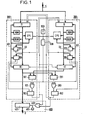
- FIG. 1 schematically represents a self-tested action automation intended for the control of an industrial installation.
- Two identical microprocessors 100 and 200 receive in parallel the signals of a common clock 300 and information 1 relating to the operation of the industrial installation and delivers commands in the direction of safety logic 400 which does not validate a modification of the commands of the installation only in case of unanimity of the two microprocessors 100, 200.
- Each microprocessor 100, 200 comprises, in a well-known manner, an input interface II by which it has access to information relating to the operation of the industrial installation and the other microprocessor, an output interface 01 by which it delivers commands, a ROM program read-only memory, a RAM calculation memory and a central processing unit CPU interconnected by a data bus DB and an address bus AD.
- the safety logic 400 is formed by a set of transfer registers 401 receiving as input the commands supplied by the output interface 01 of the microprocessor 100, delivering as output the commands 2 necessary for the operation of the industrial installation and having a transfer control connected via a logic gate of the "or" type 402 with two inputs connected to the outputs of the fault memories 102, 202 of the microprocessors 100, 200 and blocked by the arming of any of the fault memories 102, 202.
- the logic part of type "or" 402 also commands an alarm 403.
- the microprocessors 100, 200 are programmed identically with regard to the operation of the industrial installation, operation which each of them could provide alone if it were not for the safety requirement.
- the safety of the automation rests on the fact that two identical microprocessors programmed in an identical way must have identical responses to identical stresses. Any difference in behavior between the two microprocessors is, from this safety perspective, characteristic of a fault state of the automation and must lead to freezing of the commands in their states prior to the appearance of the fault. It is detected at the output interfaces 01 of the microprocessors 100, 200 by the wired comparators 101, 201.
- the wired comparator of a first microprocessor detects a difference between the commands of the first and of the second microprocessor, it blocks the logic of safety 400 which maintains the controls in their previous states, resets the output interface 01 of the second microprocessor to zero and causes, by reaction, the zeroing of the output interface 01 of the first microprocessor which perfects the blocking of the automation.
- the compatibility of the programs in execution time is easy to obtain by using a clock 300 common to the two microprocessors and by giving the latter identical programs for the control of the industrial installation.
- the lack of safety due to the non-redundancy of the clock 300 is compensated by the presence of a clock monitoring circuit 500 which can be a monostable flip-flop constantly armed, the triggering of which blocks the safety logic 400 by through the fault memories 101, 201 and which is constantly reset before being switched over by the clock signal.
- the starting of the microprocessors with the same clock microcycle and their identical interpretation of the data to be processed cannot be ensured in all eventualities, this for various reasons, in particular the parasites which can affect the two microprocessors 100, 200, the deviations between the thresholds with respect to which the microprocessors compare the same datum to determine its logical level and the deviations between the instants of sampling of the same datum during the same clock microcycle due to two differences between the paths followed by the clock signal to reach the central processing units CPU of the two microprocessors.
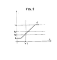
- Figure 2 illustrates one of the many possibilities where the same data can be seen differently by two microprocessors clocked by a common clock.
- Asynchronous data with respect to the clock goes from logic value 0 to logic value 1 while it is being read by the two microprocessors.
- the first microprocessor which samples it at an instant t 1 with respect to its threshold Si reads a logic value 0 while the second microprocessor which samples it at an instant t 2 with respect to its threshold S 2 reads a logical value 1.
- the thresholds Si and S 2 are naturally very close as are the times t 1 and t 2 so that such an eventuality is unlikely to occur. However, it must be guarded against so as to not lead to unjustified blockages of automation.
- a synchronization procedure for the two microprocessors is started, during which each microprocessor is periodically ordered to arm its synchronization register for a certain number of machine cycles and then to carry out two successive readings of the synchronization register of the machine.
- other microprocessor spaced by a suitable number of machine cycles, one of the microprocessors operating with a looped program of fixed length, the other with another looped program of different length possibly variable and more or less long than the length program fixed depending on whether the result of its readings shows it to be ahead or behind on the other microprocessor.
- the programs of the two microprocessors 100, 200 during their synchronization can be assimilated to the movements of two mobiles traveling around a circumference, one at constant speed, the other pursuing it.
- the chronology of the operations in search of synchronism is defined by numbers of machine cycles, that is to say of elementary cycles of operations of the microprocessors which correspond in duration to the microcycles of the clock but which have no absolute reference in relation to the latter but in relation to the program executed, any instruction taking for its execution a defined number of machine cycles.
- FIGS. 3, 4 and 5 are time diagrams illustrating the chronology of the inscriptions and readings of the synchronization registers 105, 205 of the microprocessors 100, 200 during the synchronization procedure.
- the curves a represent the signal from the clock 300
- the curves b the instants of reading by the first microprocessor 100 of the synchronization register tion 205 of the second microprocessor 200
- the curves c the logical states of the synchronization register 105 of the first microprocessor 100
- the curves f the instants of reading by the second microprocessor 200 of the synchronization register 105 of the first microprocessor 100
- the curves g the states logic of the synchronization register 205 of the second microprocessor 200.
- FIG. 3 relates to the case where the first microprocessor 100 is ahead of two clock microcytes on the second microprocessor 200.
- the first microprocessor 100 begins with two successive readings of the synchronization register 205 of the second microprocessor which are spaced by a Ni number of machine cycles and during which he does not see this register constantly armed. It then arms its synchronization register 105, N 2 machine cycles after its first reading, for N 3 + 1 machine cycles and repeats these operations N 4 machine cycles after the start of arming its synchronization register 105 because it doesn’t has not seen the synchronization register 205 of the second microprocessor 200 constantly armed.
- the second microprocessor 200 begins by arming its synchronization register 205 with a delay of two clock microcycles compared to the first reading made by the first microprocessor and keeps this register 205 armed for Ni + 1 machine cycles. It then starts, after N 2 machine cycles after arming its synchronization register 205, two readings from the synchronization register 105 of the first microprocessor spaced from N 3 machine cycles and sees this register once armed and a second time disarmed which leads him to repeat these operations a number N 6 of machine cycles after its first reading taken equal to the number (N 4 - 1 in order to reduce its delay by a clock microcycle. After two operations the two microprocessors are found in synchronism, case shown in Figure 5.
- FIG. 4 relates to the case where the first microprocessor 100 is behind by two clock microcycles on the second microprocessor 200.
- the behavior of the first microprocessor 100 remains unchanged compared to FIG. 3. That of the second is modified before the first iteration because he saw during the first two readings, the synchronization register 105 once disarmed and a second time armed which leads him to perform his first iteration a number N 6 of machine cycles after his first reading taken equal to number N 4 + 1 in order to decrease its advance by a clock microcycle. After two iterations, the two microprocessors find themselves in synchronism, case shown in FIG. 5.
- FIG. 5 shows that the chronology defined by the set of numbers of machine cycles N 1 , N 2 , N 3 implies that when one of the microprocessors sees, during its double reading, the synchronization register of the other constantly armed, it is necessarily the same for the other.
- These numbers of machine cycles are obtained by taking into account the numbers of machine cycles necessary for the arming, disarming and readings instructions of the synchronization registers as well as the instructions necessary for the interpretation of the readings of the registers and, possibly, in programming inoperative instructions as part of the operations carried out during synchronism search.
- a double reading of a synchronization register is done by having the sum of the second reading with the double of the first reading calculated by the microprocessor concerned and the analysis of this sum, a zero result implying that the microprocessor saw the synchronization register constantly disarmed, a result equal to one implying that the microprocessor saw the synchronization register a first time disarmed and a second time armed, a result equal to two implying that the microprocessor saw the register synchronized for the first time and a second time disarmed and a result equal to three implying that the microprocessor saw the synchronization register constantly armed.
- a synchronization test can be carried out which consists in commanding each microprocessor after it has seen the synchronization register of the other constantly armed during the two successive readings it performs and before that the program for operating the industrial installation does not begin, a third reading of the synchronization register of the other microprocessor during which the latter register must appear disarmed, an opposite result leading for the microprocessor concerned to a resumption of the synchronization program from the start. This third reading constitutes a test of the correct operation of the synchronization registers.
- the desynchronization of two microprocessors 100, 200 can occur following a disagreement on the interpretation of a binary data being varied. As this disagreement disappears as soon as the data has finished changing state, it is advantageous to wait for the disappearance of this disagreement so as not to have to resume from the start the program for operating the industrial installation.
- the synchronization process is completed by imposing, on each microprocessor 100, 200, during the execution of the program for controlling the industrial installation, to transfer to its output interface on specific outputs that do not deliver control but tested by comparators 101, 201, every data from the outside before using them and repeating this operation several times as long as the comparators 101, 201 detect a difference before starting the synchronization procedure described above.
- the positioning interface 104, 204 of the fault memory 102, 202 of each microprocessor 100, 200 is then used to disarm the fault memory 102, 202 between each attempt. Apart from these attempts, the positioning interface 104, 204 is used for tests of the proper functioning of the fault memory 102, 202.
Landscapes
- Engineering & Computer Science (AREA)
- Theoretical Computer Science (AREA)
- Quality & Reliability (AREA)
- Physics & Mathematics (AREA)
- General Engineering & Computer Science (AREA)
- General Physics & Mathematics (AREA)
- Multi Processors (AREA)
- Hardware Redundancy (AREA)
- Debugging And Monitoring (AREA)
- Synchronisation In Digital Transmission Systems (AREA)
- Stabilization Of Oscillater, Synchronisation, Frequency Synthesizers (AREA)
- Time-Division Multiplex Systems (AREA)
Priority Applications (1)
| Application Number | Priority Date | Filing Date | Title |
|---|---|---|---|
| AT82108541T ATE22496T1 (de) | 1981-09-22 | 1982-09-16 | Verfahren zur synchronisierung zweier mikroprozessoren. |
Applications Claiming Priority (2)
| Application Number | Priority Date | Filing Date | Title |
|---|---|---|---|
| FR8117832 | 1981-09-22 | ||
| FR8117832A FR2513409A1 (fr) | 1981-09-22 | 1981-09-22 | Procede de synchronisation de deux microprocesseurs |
Publications (2)
| Publication Number | Publication Date |
|---|---|
| EP0075278A1 EP0075278A1 (fr) | 1983-03-30 |
| EP0075278B1 true EP0075278B1 (fr) | 1986-09-24 |
Family
ID=9262353
Family Applications (1)
| Application Number | Title | Priority Date | Filing Date |
|---|---|---|---|
| EP82108541A Expired EP0075278B1 (fr) | 1981-09-22 | 1982-09-16 | Procédé de synchronisation de deux microprocesseurs |
Country Status (7)
| Country | Link |
|---|---|
| EP (1) | EP0075278B1 (enExample) |
| AT (1) | ATE22496T1 (enExample) |
| BR (1) | BR8205539A (enExample) |
| DE (1) | DE3273471D1 (enExample) |
| ES (1) | ES515854A0 (enExample) |
| FR (1) | FR2513409A1 (enExample) |
| MX (1) | MX155323A (enExample) |
Families Citing this family (5)
| Publication number | Priority date | Publication date | Assignee | Title |
|---|---|---|---|---|
| DE3332802A1 (de) * | 1983-09-12 | 1985-03-28 | Siemens AG, 1000 Berlin und 8000 München | Schaltungsanordnung zum pruefen des ordnungsgerechten anlaufens eines zweikanaligen fail-safe-mikrocomputerschaltwerkes, insbesondere fuer eisenbahnsicherungsanlagen |
| US5020024A (en) * | 1987-01-16 | 1991-05-28 | Stratus Computer, Inc. | Method and apparatus for detecting selected absence of digital logic synchronism |
| EP0394514B1 (de) * | 1989-04-25 | 1994-07-13 | Siemens Aktiengesellschaft | Verfahren zur Synchronisation von Datenverarbeitungsanlagen |
| JPH04133102A (ja) * | 1990-09-26 | 1992-05-07 | Mitsubishi Electric Corp | プログラマブル・コントローラ及びその制御方法 |
| DE19809089A1 (de) * | 1998-02-25 | 1999-08-26 | Siemens Ag | Synchronisations- und/oder Datenaustauschverfahren für sichere, hochverfügbare Rechner und hierzu geeignete Einrichtung |
Citations (1)
| Publication number | Priority date | Publication date | Assignee | Title |
|---|---|---|---|---|
| DE2651314B1 (de) * | 1976-11-10 | 1977-12-08 | Siemens Ag | Sicherheits-Ausgabeschaltung fuer eine Binaersignale abgebende Datenverarbeitungsanlage |
Family Cites Families (3)
| Publication number | Priority date | Publication date | Assignee | Title |
|---|---|---|---|---|
| DE1269827B (de) * | 1965-09-09 | 1968-06-06 | Siemens Ag | Verfahren und Zusatzeinrichtung zur Synchronisierung von parallel arbeitenden Datenverarbeitungsanlagen |
| US3810119A (en) * | 1971-05-04 | 1974-05-07 | Us Navy | Processor synchronization scheme |
| DE2458224C3 (de) * | 1974-12-09 | 1978-04-06 | Siemens Ag, 1000 Berlin Und 8000 Muenchen | Datenverarbeitungssystem mit Koordinierung der Parallelarbeit von mindestens zwei Datenverarbeitungsanlagen |
-
1981
- 1981-09-22 FR FR8117832A patent/FR2513409A1/fr active Granted
-
1982
- 1982-09-16 DE DE8282108541T patent/DE3273471D1/de not_active Expired
- 1982-09-16 EP EP82108541A patent/EP0075278B1/fr not_active Expired
- 1982-09-16 AT AT82108541T patent/ATE22496T1/de active
- 1982-09-21 BR BR8205539A patent/BR8205539A/pt not_active IP Right Cessation
- 1982-09-21 ES ES515854A patent/ES515854A0/es active Granted
- 1982-09-21 MX MX194473A patent/MX155323A/es unknown
Patent Citations (1)
| Publication number | Priority date | Publication date | Assignee | Title |
|---|---|---|---|---|
| DE2651314B1 (de) * | 1976-11-10 | 1977-12-08 | Siemens Ag | Sicherheits-Ausgabeschaltung fuer eine Binaersignale abgebende Datenverarbeitungsanlage |
Also Published As
| Publication number | Publication date |
|---|---|
| FR2513409B1 (enExample) | 1983-12-02 |
| EP0075278A1 (fr) | 1983-03-30 |
| FR2513409A1 (fr) | 1983-03-25 |
| BR8205539A (pt) | 1983-08-30 |
| DE3273471D1 (en) | 1986-10-30 |
| ES8306539A1 (es) | 1983-06-01 |
| MX155323A (es) | 1988-02-18 |
| ATE22496T1 (de) | 1986-10-15 |
| ES515854A0 (es) | 1983-06-01 |
Similar Documents
| Publication | Publication Date | Title |
|---|---|---|
| FR2666425A1 (fr) | Procede et dispositif de mise a jour d'informations dans une memoire et leur utilisation dans les cartes a memoire. | |
| CA2480896C (fr) | Procede de securisation d'une entite electronique a acces crypte | |
| EP0044039A1 (fr) | Objet portatif individualisé du genre carte de crédit | |
| FR2692701A1 (fr) | Procédé de contrôle de configuration d'une installation complexe et dispositif pour la mise en Óoeuvre de ce procédé. | |
| EP0075278B1 (fr) | Procédé de synchronisation de deux microprocesseurs | |
| FR2477738A1 (fr) | Appareil de commande et de controle destine a etre utilise entre un poste central de calculateur et des postes terminaux | |
| EP1120662B1 (fr) | Procédé pour tester un circuit intégré comportant des parties matérielles et/ou logicielles ayant un caractère de confidentialité | |
| FR2528196A1 (fr) | Appareil de protection de programmes d'ordinateur | |
| EP0161177A1 (fr) | Procédé et dispositif de récupération de mot de verrouillage de trame à bits répartis dans un signal numérique | |
| FR2643478A1 (fr) | Carte a circuit integre | |
| FR2632092A1 (fr) | Circuit de conditionnement d'ecriture d'antememoire retarde pour un systeme de microcalculateur a bus double comprenant une unite 80386 et une unite 82385 | |
| FR3038188A1 (fr) | Systeme de verification de l’integrite d’une communication entre deux circuits | |
| EP0249930A1 (fr) | Procédé de synchronisation de deux trains binaires | |
| EP0115222B1 (fr) | Procédé pour assurer la sécurité du fonctionnement d'un automate programmable et automate pour la mise en oeuvre du procédé | |
| EP0168330B1 (fr) | Dispositif de cadrage automatique d'horloge locale par rapport à un signal de données et circuit d'échantillonnage en comportant application | |
| FR2884329A1 (fr) | Protection de donnees d'une memoire associee a un microprocesseur | |
| FR2569323A1 (fr) | Dispositif d'adaptation plesiochrone | |
| FR2749697A1 (fr) | Procede de mise en oeuvre d'un appareil de commande avec une memoire programmee par un dispositif de programmation | |
| FR2498035A1 (fr) | Procede et dispositif de synchronisation de messages | |
| EP3182286A1 (fr) | Procede de verification de fonctionnalites d'un logiciel destine a etre embarque dans un composant cryptographique, systeme | |
| FR2707773A1 (fr) | Circuit intégré du type microcontroleur à mémoire morte masquée contenant un programme générique de test, station de test et procédé de fabrication correspondants. | |
| FR2634918A1 (fr) | Dispositif de detection d'erreur et de memorisation d'informations d'erreur et procede de mise en evidence | |
| FR2788353A1 (fr) | Microprocesseur avec circuits de protection pour securiser l'acces a ses registres | |
| EP0172797A1 (fr) | Séquenceur transitionel programmable | |
| WO2013153167A1 (fr) | Dispositif pour générer une signature à l'exécution d'une tâche de programme et méthode de comparaison de flots d'exécution |
Legal Events
| Date | Code | Title | Description |
|---|---|---|---|
| PUAI | Public reference made under article 153(3) epc to a published international application that has entered the european phase |
Free format text: ORIGINAL CODE: 0009012 |
|
| AK | Designated contracting states |
Designated state(s): AT BE CH DE FR GB IT LI LU NL SE |
|
| 17P | Request for examination filed |
Effective date: 19830908 |
|
| GRAA | (expected) grant |
Free format text: ORIGINAL CODE: 0009210 |
|
| AK | Designated contracting states |
Kind code of ref document: B1 Designated state(s): AT BE CH DE FR GB IT LI LU NL SE |
|
| REF | Corresponds to: |
Ref document number: 22496 Country of ref document: AT Date of ref document: 19861015 Kind code of ref document: T |
|
| REF | Corresponds to: |
Ref document number: 3273471 Country of ref document: DE Date of ref document: 19861030 |
|
| ITF | It: translation for a ep patent filed | ||
| PLBE | No opposition filed within time limit |
Free format text: ORIGINAL CODE: 0009261 |
|
| STAA | Information on the status of an ep patent application or granted ep patent |
Free format text: STATUS: NO OPPOSITION FILED WITHIN TIME LIMIT |
|
| 26N | No opposition filed | ||
| PGFP | Annual fee paid to national office [announced via postgrant information from national office to epo] |
Ref country code: GB Payment date: 19930825 Year of fee payment: 12 |
|
| PGFP | Annual fee paid to national office [announced via postgrant information from national office to epo] |
Ref country code: SE Payment date: 19930922 Year of fee payment: 12 Ref country code: DE Payment date: 19930922 Year of fee payment: 12 Ref country code: CH Payment date: 19930922 Year of fee payment: 12 |
|
| ITTA | It: last paid annual fee | ||
| PGFP | Annual fee paid to national office [announced via postgrant information from national office to epo] |
Ref country code: NL Payment date: 19930930 Year of fee payment: 12 Ref country code: FR Payment date: 19930930 Year of fee payment: 12 Ref country code: AT Payment date: 19930930 Year of fee payment: 12 |
|
| PGFP | Annual fee paid to national office [announced via postgrant information from national office to epo] |
Ref country code: LU Payment date: 19931015 Year of fee payment: 12 |
|
| PGFP | Annual fee paid to national office [announced via postgrant information from national office to epo] |
Ref country code: BE Payment date: 19931022 Year of fee payment: 12 |
|
| EPTA | Lu: last paid annual fee | ||
| PG25 | Lapsed in a contracting state [announced via postgrant information from national office to epo] |
Ref country code: LU Free format text: LAPSE BECAUSE OF NON-PAYMENT OF DUE FEES Effective date: 19940916 Ref country code: GB Effective date: 19940916 Ref country code: AT Effective date: 19940916 |
|
| PG25 | Lapsed in a contracting state [announced via postgrant information from national office to epo] |
Ref country code: SE Effective date: 19940917 |
|
| PG25 | Lapsed in a contracting state [announced via postgrant information from national office to epo] |
Ref country code: LI Effective date: 19940930 Ref country code: CH Effective date: 19940930 Ref country code: BE Effective date: 19940930 |
|
| EAL | Se: european patent in force in sweden |
Ref document number: 82108541.2 |
|
| BERE | Be: lapsed |
Owner name: CGEE ALSTHOM Effective date: 19940930 |
|
| PG25 | Lapsed in a contracting state [announced via postgrant information from national office to epo] |
Ref country code: NL Effective date: 19950401 |
|
| GBPC | Gb: european patent ceased through non-payment of renewal fee |
Effective date: 19940916 |
|
| NLV4 | Nl: lapsed or anulled due to non-payment of the annual fee | ||
| PG25 | Lapsed in a contracting state [announced via postgrant information from national office to epo] |
Ref country code: FR Effective date: 19950531 |
|
| REG | Reference to a national code |
Ref country code: CH Ref legal event code: PL |
|
| PG25 | Lapsed in a contracting state [announced via postgrant information from national office to epo] |
Ref country code: DE Effective date: 19950601 |
|
| EUG | Se: european patent has lapsed |
Ref document number: 82108541.2 |
|
| REG | Reference to a national code |
Ref country code: FR Ref legal event code: ST |