EP0073348A1 - Steckverbindungsanordnung zur Zu- und Herausführung vieladriger Kabel zur Verbindung elektrischer Baueinheiten untereinander - Google Patents
Steckverbindungsanordnung zur Zu- und Herausführung vieladriger Kabel zur Verbindung elektrischer Baueinheiten untereinander Download PDFInfo
- Publication number
- EP0073348A1 EP0073348A1 EP82106886A EP82106886A EP0073348A1 EP 0073348 A1 EP0073348 A1 EP 0073348A1 EP 82106886 A EP82106886 A EP 82106886A EP 82106886 A EP82106886 A EP 82106886A EP 0073348 A1 EP0073348 A1 EP 0073348A1
- Authority
- EP
- European Patent Office
- Prior art keywords
- plug
- housing
- arrangement according
- plug housing
- connector
- Prior art date
- Legal status (The legal status is an assumption and is not a legal conclusion. Google has not performed a legal analysis and makes no representation as to the accuracy of the status listed.)
- Granted
Links
Images


Classifications
-
- H—ELECTRICITY
- H01—ELECTRIC ELEMENTS
- H01R—ELECTRICALLY-CONDUCTIVE CONNECTIONS; STRUCTURAL ASSOCIATIONS OF A PLURALITY OF MUTUALLY-INSULATED ELECTRICAL CONNECTING ELEMENTS; COUPLING DEVICES; CURRENT COLLECTORS
- H01R13/00—Details of coupling devices of the kinds covered by groups H01R12/70 or H01R24/00 - H01R33/00
- H01R13/62—Means for facilitating engagement or disengagement of coupling parts or for holding them in engagement
- H01R13/627—Snap or like fastening
- H01R13/6271—Latching means integral with the housing
-
- H—ELECTRICITY
- H01—ELECTRIC ELEMENTS
- H01R—ELECTRICALLY-CONDUCTIVE CONNECTIONS; STRUCTURAL ASSOCIATIONS OF A PLURALITY OF MUTUALLY-INSULATED ELECTRICAL CONNECTING ELEMENTS; COUPLING DEVICES; CURRENT COLLECTORS
- H01R13/00—Details of coupling devices of the kinds covered by groups H01R12/70 or H01R24/00 - H01R33/00
- H01R13/62—Means for facilitating engagement or disengagement of coupling parts or for holding them in engagement
- H01R13/629—Additional means for facilitating engagement or disengagement of coupling parts, e.g. aligning or guiding means, levers, gas pressure electrical locking indicators, manufacturing tolerances
- H01R13/633—Additional means for facilitating engagement or disengagement of coupling parts, e.g. aligning or guiding means, levers, gas pressure electrical locking indicators, manufacturing tolerances for disengagement only
Definitions
- the invention relates to a plug arrangement for feeding in and out multi-core cables for connecting electrical units to one another, in particular for connecting the central unit of a data processing system to its peripheral devices.
- the central unit of a data processing system is in many cases to be connected to a large number of peripheral devices, for example a keyboard, a printer, a magnetic disk memory and the like, or a central unit must be connected to a large number of data terminals, for example consist of a keyboard and a display device.
- peripheral devices for example a keyboard, a printer, a magnetic disk memory and the like
- data terminals for example consist of a keyboard and a display device.
- the invention aims to provide a connector arrangement which is as practical as possible for the connection of such structural units to one another, such that the plug contact connections can be attached as close as possible to one another on the central unit. So that they take up as little space as possible, it is necessary to design them in such a way that they can be mounted as closely as possible in matrix form. Furthermore, it is desirable not to perform the decoupling of the lines of the central unit from the lines of the peripheral devices and the radio interference suppression within the device housing, but rather to connect them to the plug arrangement as possible, so that the decoupling also occurs when the plug arrangement is inserted and removed and the radio interference suppression is carried out. This design assumes that a number of electrical components in the connector assembly must be present, which are of course arranged on a circuit board. Another application of the connector arrangement is given when connecting peripheral devices to adapt the physical interface.
- connector assemblies which are only held in their sockets by a clamping action, has not proven particularly useful in this context, because the large number of conductors to be connected together results in relatively large connectors and then a relatively large amount of force is required to remove the connectors to pull out of their clamping sockets.
- the connector arrangements which only work with a clamping effect, can only be arranged at a relatively large distance from one another in the mounting plates, because it is necessary to grip with the whole hand in order to pull out the connector.
- the connector arrangement according to the invention is intended to create a connecting means which can be relatively easily pulled out of the socket and also inserted again.
- the connector arrangement according to the invention is characterized in that in a connector housing a circuit board carrying the electrical components and the plug contacts is connected to a holding part, relative to which the connector housing is movable against the force of a spring.
- the connector housing can be locked by means of locking projections with corresponding recesses in a fixedly arranged socket part, in which the mating contacts are also arranged and in which a spring presses the connector housing into the removal position when the locking is released by pressure on the connector housing .
- the relative displaceability of the circuit board with the contacts and the plug housing relative to one another ensures that, despite the displacement of the switch housing to release the latching, the contacts easily engage with one another and can also be pulled out again.
- Another advantage of the connector arrangement is that there is sufficient space in the connector housing provided as a rectangular component for accommodating additional components for decoupling, radio interference suppression or interface adaptation, etc., the rectangular design also having the advantage of being as closely aligned as possible to enable the connector arrangements in a device wall.
- the connector housing consists of a bottom part for the storage of the holding plate and the circuit board and a cover, it is possible to provide not only one circuit board but even several and then to close the connector housing with a higher cover. This makes it possible to accommodate additional electrical components and even possibly to realize additional functions without the dimensions of the connector arrangement changing significantly.
- the attachment of the electrical line with the holding part ensures that a train on the line does not lead to an unwanted unlocking.
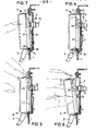
- a holding rail 1 or a frame On the rear wall or a side wall of an electrical device which is to be connected to various other electrical devices, for example, a holding rail 1 or a frame is arranged, which is provided with openings 2, in which the individual plug arrangements are mounted.
- a socket part 3 is assigned to each plug arrangement.
- the plug housing 6 is locked in the socket part 3.
- the socket part 3 rests with its edges 4 on the holding rail 1 and is screwed to it.
- the electrical connection cables 5 are led out downwards.
- FIG. 1 now shows an exploded view of a plug arrangement according to the invention, which consists of a socket part 3 and a plug housing 6.
- the plug housing 6 comprises a bottom part 7 on the one hand and a cover 8 on the other hand.
- the bottom part 7 has at its upper end a latching lug 9 which engages in a recess 10 in the socket part 3 when the plug housing is inserted.
- a leg spring 11 attached, which protrude with the help of two bent ends 12 of their legs in the rectangular recessed interior 13 of the socket part 3.
- a plug contact arrangement 14 is provided, to which the electrical lines are led, which are to be led out of the device or which have to be inserted into the device.
- a further recess 15 is provided, which cooperates with a locking projection 16 on a holding part 17.
- the holding part 17 is guided in the bottom part 7 of the connector housing 6 on the one hand through a recess in the bottom, and on the other hand through a tab 18 which is fastened to the bottom part 7.
- a pin-slot connection 19 secures the lateral position of the holding part 17, but allows a relative movement between the bottom part 7 and the holding part 17.
- a spring 20 is fastened at 21 and presses on the holding part 17 via a projection 22, so that the pin-slot connection 19 is in the position shown (FIG. 3). If one presses on the plug housing 6 from above, the housing can move relative to the holding plate 7. The displacement distance results from the difference between the dimension a according to FIG. 4 and 7 and b according to FIG. 5 and 6.
- both the base part 7 and the holding plate 17 are provided with a corresponding opening 23, 24, so that the contacts 25 on the switching plate 26 can be inserted into the mating contacts 14 through the cutouts 23 and 24.
- the holding plate 17 and the circuit board 26 can be screwed together, so that these two parts can then be moved together relative to the plug housing 6.
- the connector housing 6 can be closed with the aid of a cover 8.
- a second one Circuit board 29 are used, and in this case, a higher cover 8 ', as shown in dash-dotted lines in FIG. 1 is indicated used.
- FIG. 4 shows the plug housing 6 in its position locked in the socket part 3.
- the contacts 14 and 25 are in engagement with each other, the leg spring 11 is tensioned by the bottom part 7 of the connector housing 6.
- the nose 9 on the bottom part 7 has penetrated into the recess 10 of the socket part 3.
- the locking projection 16 is engaged on the holding part 17 in the recess 15 of the socket part 3.
- the holding part 17 is also provided with a stop 30, which is supported in the socket part 3.
- FIG. 5 shows, on the upper edge of the connector housing 6, then the housing moves relative to the holding plate 17 and the switching plate 26 by the difference between the dimension a and the dimension b, the nose 9 on the connector housing 6 comes out of engagement with the recess 10, which is further supported by the bent ends 12 of the leg spring 11, so that the plug part 6 initially the position shown in FIG. 5 and then the position shown in FIG. 6 occupies, in which the connector housing 6 can now be easily removed by lifting it up slightly so that the locking projection 16 and the recess 15 come out of engagement with one another.
- FIG. 5 reveals remains during the displacement of the connector housing 6 from the position shown in FIG. 4 in the position shown in FIG. 5, the contact arrangement 14, 25 is still fully engaged. The electrical connection is only interrupted when the plug part 6 then tilts forward.
- the lug 9 is rounded off on the plug housing 6, whereby the engagement of the plug housing 6 with the socket 3 is facilitated.
Abstract
Description
- Die Erfindung bezieht sich auf eine Steckeranordnung zur Zu-und Herausführung vieladriger Kabel zur Verbindung elektrischer Baueinheiten untereinander, insbesondere zur Verbindung der Zentraleinheit einer Datenverarbeitungsanlage mit ihren peripheren Geräten.
- Die Zentraleinheit einer Datenverarbeitungsanlage ist in vielen Fällen mit einer großen Vielzahl von peripheren Geräten zu verbinden, beispielsweise mit einer Tastatur, mit einem Drucker, mit einem Magnetplattenspeicher und dergl., oder aber eine Zentraleinheit muß mit einer großen Vielzahl von Datenendstationen verbunden sein, die beispielsweise aus einer Tastatur und einem Bildschirmgerät bestehen.
- Die Erfindung zielt darauf ab, eine möglichst praktisch zu handhabende Steckeranordnung für die Verbindung derartiger Baueinheiten untereinander zu schaffen, derart daß die Steckkontaktverbindungen möglichst dicht beieinander an der Zentraleinheit angebracht werden können. Damit sie möglichst wenig Platz beanspruchen, ist es notwendig, sie so auszubilden, daß sie in Matrixform möglichst eng beieinander liegend montiert werden können. Ferner ist es wünschenswert, die Entkopplung der Leitungen der Zentraleinheit von den Leitungen der peripheren Geräte sowohl als auch die Funkentstörung nicht innerhalb der Gerätegehäuse durchzuführen, sondern sie möglichst mit der Steckanordnung zu verbinden, so daß gleichzeitig mit dem Einstecken und Herausziehen der Steckeranordnung auch die Entkopplung und die Funkentstörung durchgeführt wird. Diese Bauweise setzt es voraus, daß in der Steckeranordnung eine Anzahl von elektrischen Bauteilen vorhanden sein muß, die selbstverständlich auf einer Schaltplatte angeordnet werden. Eine weitere Anwendung der Steckeranordnung ist gegeben beim Anschluß von Peripheriegeräten zum Anpassen der physikalischen Schnittstelle.
- Die Verwendung von Steckeranordnungen, die lediglich durch Klemmwirkung in ihren Steckbuchsen gehalten werden, hat sich in diesem Zusammenhange nicht besonders bewährt, weil bei der Vielzahl der miteinander zu verbindenden Leiter relativ große Stecker entstehen und weil es dann eines relativ großen Kraftaufwandes bedarf, um die Stecker aus ihren klemmenden Steckbuchsen herauszuziehen. Aus diesem Grunde können auch die lediglich mit Klemmwirkung arbeitenden Steckeranordnungen nur mit relativ großem Abstand zueinander in den Montageplatten angeordnet werden, weil es notwendig ist, mit der ganzen Hand zuzufassen, um den Stecker herauszuziehen. Demgegenüber soll durch die erfindungsgemäße Steckeranordnung ein Verbindungsmittel geschaffen werden, welches sich relativ leicht aus der Steckbuchse herausziehen und auch wieder hereinstecken läßt.
- Die erfindungsgemäße Steckeranordnung ist dadurch gekennzeichnet, daß in einem Steckergehäuse eine die elektrischen Bauteile und die Steckkontakte tragende Schaltplatte mit einem Halteteil verbunden ist, relativ zu welchem das Steckergehäuse entgegen der Kraft einer Feder beweglich ist.
- Gemäß einem weiteren Merkmal der Erfindung ist das Steckergehäuse mittels Rastvorsprüngen mit entsprechenden Ausnehmungen in einem fest angeordneten Buchsenteil verrastbar, in dem auch die Gegenkontakte angeordnet sind und bei dem eine Feder das Steckergehäuse in die Entnahmestellung drückt, wenn die Verrastung durch Druck auf das Steckergehäuse gelöst wird.
- Bei einer derartigen Ausbildung des Steckergehäuses ist es möglich, durch einfachen Druck auf das Steckergehäuse mit einem Finger dieses zunächst aus seiner Verrastung zu lösen, so daß es dann in die Entnahmestellung gedrückt wird und herausgezogen werden kann, ohne daß hierfür ein besonderer Kraftaufwand erforderlich wäre.
- Durch die relative Verschiebbarkeit der Schaltplatte mit den Kontakten und des Steckergehäuses zueinander wird sichergestellt, daß trotz Verschiebung des Schaltergehäuses zum Lösen der Verrastung die Kontakte problemlos miteinander in Eingriff kommen und auch wieder herausgezogen werden können. Ein weiterer Vorteil der Steckeranordnung ist es, daß in dem als rechteckiges Bauteil vorgesehenen Steckergehäuse ausreichend Platz vorhanden ist für die Unterbringung zusätzlicher Bauteile für die Entkopplung, die Funkentstörung bzw. Schnittstellenanpassung usw., wobei die rechteckige Bauform gleichzeitig den Vorteil hat, eine möglichst enge Aneinanderreihung der Steckeranordnungen in einer Gerätewand zu ermöglichen.
- Dadurch daß das Steckergehäuse aus einem Bodenteil für die Lagerung der Halteplatte und der Schaltplatte und aus einem Deckel besteht, ist es möglich, nicht nur eine Schaltplatte sondern sogar mehrere vorzusehen und das Steckergehäuse dann mit einem höheren Deckel zu verschließen. Hierdurch wird es möglich, zusätzliche elektrische Bauteile unterzubringen und sogar evtl. weitere Funktionen zu verwirklichen, ohne daß sich die Dimensionen der Steckeranordnung wesentlich ändern. Durch die Befestigung der elektrischen Leitung mit dem Halteteil ist sichergestellt, daß ein Zug auf die Leitung nicht zu einer ungewollten Entriegelung führt.
- In den beiliegenden Zeichnungen ist ein Ausführungsbeispiel der Erfindung gezeigt.
- FIG. 1 ist eine Explosivdarstellung der erfindungsgemäßen Steckeranordnung,
- FIG. 2 zeigt eine Vorderansicht des Steckbuchsenteiles,
- FIG. 3 ist eine Ansicht des Bodenteiles des Steckergehäuses mit Halteteil,
- FIG. 4 zeigt die Steckeranordnung in fertig montiertem Zustande,
- FIG. 5 und 6 zeigen das Herausnehmen des Steckers,
- FIG. 7 zeigt das Einführen des Steckers,
- FIG. 8 zeigt die matrixförmige Anordnung der Stecker in einer entsprechenden Halteschiene, die beispielsweise an der Rückseite des mit verschiedenen anderen Geräten zu verbindenden elektrischen Gerätes vorgesehen ist.
- An der Rückwand oder einer Seitenwand eines elektrischen Gerätes , welches mit verschiedenen anderen elektrischen Geräten verbunden werden soll, sei beispielsweise eine Halteschiene 1 bzw. ein Rahmen angeordnet, der mit Durchbrüchen 2 versehen ist, in denen die einzelnen Steckeranordnungen montiert werden. Jeder Steckeranordnung ist ein Buchsenteil 3 zugeordnet. In dem Steckbuchsenteil 3 ist das Steckergehäuse 6 verrastet. Das Steckbuchsenteil 3 liegt mit seinen Rändern 4 auf der Halteschiene 1 auf und ist damit verschraubt. Die elektrischen Verbindungskabel 5 sind nach unten herausgeführt.
- FIG. 1 zeigt nun in Explosivdarstellung eine erfindungsgemäße Steckeranordnung, die aus einem Steckbuchsenteil 3 und aus einem Steckergehäuse 6 besteht. Das Steckergehäuse 6 umfaßt einerseits ein Bodenteil 7 und andererseits einen Dekkel 8. Das Bodenteil 7 hat an seinem oberen Ende eine Rastnase 9, die in eine Ausnehmung 10 im Buchsenteil 3 einrastet, wenn das Steckergehäuse eingesetzt ist. In dem Steckbuchsenteil 3 ist auch eine Schenkelfeder 11 befestigt, die mit Hilfe von zwei abgebogenen Enden 12 ihrer Schenkel in den rechteckig ausgenommenen Innraum 13 des Steckbuchsenteiles 3 hineinragen. In der Wandung des Steckbuchsenteiles 3 ist eine Steckkontaktanordnung 14 vorgesehen, an die die elektrischen Leitungen herangeführt sind, die aus dem Gerät herauszuführen sind bzw. die in das Gerät eingeführt werden müssen. Am Boden der rechteckigen Ausnehmung 13 des Steckbuchsenteiles 3 ist eine weitere Ausnehmung 15 vorgesehen, die mit einem Rastvorsprung 16 an einem Halteteil 17 zusammenwirkt. Das Halteteil 17 ist in dem Bodenteil 7 des Steckergehäuses 6 einerseits durch eine Ausnehmung im Boden geführt, andererseits durch eine Lasche 18, die am Bodenteil 7 befestigt ist. Eine Stift-Schlitz-Verbindung 19 sichert die seitliche Lage des Halteteiles 17, läßt aber eine relative Bewegung zwischen dem Bodenteil 7 und dem Halteteil 17 zu. Eine Feder 20 ist bei 21 befestigt und drückt über einen Vorsprung 22 auf das Halteteil 17, so daß die Stift-Schlitz-Verbindung 19 sich in der gezeichneten Lage (FIG. 3) befindet. Wenn man von oben auf das Steckergehäuse 6 drückt, kann sich das Gehäuse relativ zu der Halteplatte 7 verschieben. Der Verschiebeweg ergibt sich aus der Differenz zwischen dem Maß a gemäß FIG. 4 und 7 und b gemäß FIG. 5 und 6.
- Zur Durchführung der Kontakte 14 ist sowohl das Bodenteil 7 als auch die Halteplatte 17 mit einer entsprechenden öffnung 23, 24 versehen, so daß die Kontakte 25 an der Schaltplatte 26 in die Gegenkontakte 14 eingesteckt werden können durch die Ausschnitte 23 und 24 hindurch. Mittels Schrauben 27 und Löcher 28 können die Halteplatte 17 und die Schaltungsplatte 26 miteinander verschraubt werden, so daß diese beiden Teile dann zusammen relativ zu dem Steckergehäuse 6 beweglich sind.
- Das Steckergehäuse 6 kann mit Hilfe eines Deckels 8 verschlossen werden. Im Falle daß eine Schaltplatte 26 für die Aufnahme aller benötigten Bauteile nicht ausreicht, kann eine zweite Schaltungsplatte 29 Verwendung finden, und in diesem Falle wird auch ein höherer Deckel 8', wie dies in strichpunktierten Linien in FIG. 1 angedeutet ist, verwendet.
- FIG. 4 zeigt das Steckergehäuse 6 in seiner in das Steckbuchsenteil 3 eingerasteten Position. Die Kontakte 14 und 25 befinden sich im Eingriff miteinander, die Schenkelfeder 11 ist durch das Bodenteil 7 des Steckergehäuses 6 gespannt. Die Nase 9 am Bodenteil 7 ist in die Ausnehmung 10 des Steckbuchsenteiles 3 eingedrungen. Gleichfalls ist der Rastvorsprung 16 an dem Halteteil 17 in die Ausnehmung 15 des Steckbuchsenteiles 3 eingerastet. Das Halteteil 17 ist noch mit einem Anschlag 30 versehen, der sich in dem Steckbuchsenteil 3 abstützt.
- Drückt man nun, wie die FIG. 5 zeigt, auf die obere Kante des Steckergehäuses 6, dann verschiebt sich das Gehäuse relativ zu der Halteplatte 17 und der Schaltplatte 26 um die Differenz zwischen dem Maß a und dem Maß b, die Nase 9 an dem Steckergehäuse 6 kommt außer Eingriff mit der Ausnehmung 10, was durch die abgebogenen Enden 12 der Schenkelfeder 11 noch unterstützt wird, so daß das Steckerteil 6 zunächst die Stellung gemäß FIG. 5 und dann die Stellung gemäß FIG. 6 einnimmt, in der nun das Steckergehäuse 6 leicht entnommen werden kann, indem man es etwas anhebt, so daß der Rastvorsprung 16 und die Ausnehmung 15 außer Eingriff miteinander kommen. Wie FIG. 5 erkennen läßt, bleibt während des-Verschiebens des Steckergehäuses 6 aus der Stellung gemäß FIG. 4 in die Stellung gemäß FIG. 5 die Kontaktanordnung 14, 25 noch völlig miteinander in Eingriff. Lediglich wenn dann das Steckerteil 6 nach vorne herauskippt, wird die elektrische Verbindung unterbrochen.
- Das Einsetzen des Steckers ergibt sich aus FIG. 7. Man führt zunächst den Rastvorsprung 16 in die Ausnehmung 15 im Buchsenteil ein und drückt dann leicht auf das Steckergehäuse 6, wobei wiederum eine Verschiebung des Gehäuses relativ zu der Kontaktanordnung 14, 25 erfolgt, so daß das Ineingriffgehen der beiden Kontaktanordnungen keinerlei Schwierigkeiten bereitet. Lediglich durch leichten Druck mit einem Finger auf das Steckergehäuse 6 kann die Anordnung wieder in den betriebsbereiten Zustand versetzt werden, der sich aus FIG. 4 ergibt.
- Es sei noch darauf hingewiesen, daß die Nase 9 am Steckergehäuse 6 abegrundet ist, wodurch das Ineingriffbringen des Steckergehäuses 6 mit der Steckbuchse 3 erleichtert wird.
Claims (9)
daß in einem Steckergehäuse (6) eine die elektrischen Bauteile und die Steckkontakte (25) tragende Schaltplatte (26) mit einem Halteteil (17) verbunden ist, relativ zu welchem das Steckergehäuse (6) entgegen der Kraft einer Feder (20) beweglich ist.
daß das Steckergehäuse (6) mittels Rastvorsprüngen (9, 16) mit entsprechenden Ausnehmungen (lo, 15) in einem fest angeordneten Steckbuchsenteil (3) verrastbar ist, in dem auch die Gegenkontakte (14) angeordnet sind, und daß eine Feder (11) das Steckergehäuse in die Entnahmestellung drückt, wenn die Verrastung durch Druck auf das Steckergehäuse (6) gelöst ist.
daß die Schaltplatte (26) außer den Kontakten (25) für den Anschluß der Verbindungsleitungen noch elektrische Bauteile für die Funkentstörung, die Entkopplung der Teil- .geräte der Anlage untereinander oder für Anpassungsschaltungen trägt.
daß das Steckergehäuse (6) aus einem Bodenteil (7) und einem Deckel (8) besteht, wobei das Bodenteil (7) die Schaltplatte (26) und die Halteplatte (17) trägt sowie die die Relativverschiebung des Steckergehäuses (6) und der Halteplatte (14) zueinander ermöglichende Feder (2o).
daß bei Anordnung von zwei Schaltungsplatten (26, 29) in Verbindung mit der Halteplatte (17) Deckel (8) unterschiedlicher Höhe Verwendung finden.
daß das Steckergehäuse (6) und das Steckbuchsenteil (3) rechteckigen Querschnitt haben.
daß ein Rastvorsprung (16) und ein Anschlag (30) am Halteteil (17) vorgesehen sind, welches verschieblich im Bodenteil (7) angeordnet ist und von der Feder (20) beeinflußt wird.
daß das Steckbuchsenteil (3) in einer rechteckförmigen Vertiefung zur Verrastung des Steckergehäuses die erforderlichen Ausnehmungen (10, 15) hat und mittels vorspringender Ränder in Matrixform in entsprechenden Halteschienen an den elektrisch zu verbindenden Geräten verbunden werden.
daß das elektrische Verbindungskabel (5) aus dem Steckergehäuse nach unten schräg herausgeführt ist.
Priority Applications (1)
| Application Number | Priority Date | Filing Date | Title |
|---|---|---|---|
| AT82106886T ATE13473T1 (de) | 1981-08-22 | 1982-07-30 | Steckverbindungsanordnung zur zu- und herausfuehrung vieladriger kabel zur verbindung elektrischer baueinheiten untereinander. |
Applications Claiming Priority (2)
| Application Number | Priority Date | Filing Date | Title |
|---|---|---|---|
| DE3133281A DE3133281C2 (de) | 1981-08-22 | 1981-08-22 | Steckeranordnung zur Zu- und Herausführung vieladriger Kabel zur Verbindung elektrischer Baueinheiten untereinander |
| DE3133281 | 1981-08-22 |
Publications (2)
| Publication Number | Publication Date |
|---|---|
| EP0073348A1 true EP0073348A1 (de) | 1983-03-09 |
| EP0073348B1 EP0073348B1 (de) | 1985-05-22 |
Family
ID=6139899
Family Applications (1)
| Application Number | Title | Priority Date | Filing Date |
|---|---|---|---|
| EP82106886A Expired EP0073348B1 (de) | 1981-08-22 | 1982-07-30 | Steckverbindungsanordnung zur Zu- und Herausführung vieladriger Kabel zur Verbindung elektrischer Baueinheiten untereinander |
Country Status (3)
| Country | Link |
|---|---|
| EP (1) | EP0073348B1 (de) |
| AT (1) | ATE13473T1 (de) |
| DE (2) | DE3133281C2 (de) |
Cited By (4)
| Publication number | Priority date | Publication date | Assignee | Title |
|---|---|---|---|---|
| EP0156033A2 (de) * | 1984-03-02 | 1985-10-02 | Robert Bosch Gmbh | Vielpolige Steckvorrichtung |
| DE3436968A1 (de) * | 1984-10-09 | 1986-04-10 | Leopold Kostal GmbH & Co KG, 5880 Lüdenscheid | Elektrische kupplung |
| FR2698492A1 (fr) * | 1992-11-20 | 1994-05-27 | Itw Fastex Italia Spa | Bloc intégré à câble et plaque à bornes. |
| EP0891012A2 (de) * | 1997-07-09 | 1999-01-13 | Siemens Aktiengesellschaft | Elektrische Steckvorrichtung |
Citations (4)
| Publication number | Priority date | Publication date | Assignee | Title |
|---|---|---|---|---|
| GB185090A (en) * | 1921-08-22 | 1923-08-16 | Benjamin Electric Ltd | Improvements in connecting and supporting devices for electric fixtures |
| GB474735A (en) * | 1937-05-27 | 1937-11-05 | Carr Fastener Co Ltd | Improvements in and relating to electrical connectors for use in plug and socket couplings |
| US2626974A (en) * | 1949-09-16 | 1953-01-27 | Pyle National Co | Explosion proof plug and socket |
| US2710384A (en) * | 1949-07-08 | 1955-06-07 | Burndy Engineering Co Inc | Spring loaded disconnecting panel |
Family Cites Families (6)
| Publication number | Priority date | Publication date | Assignee | Title |
|---|---|---|---|---|
| US2899669A (en) * | 1959-08-11 | Electrical connector | ||
| DE1850455U (de) * | 1959-10-22 | 1962-04-26 | Hirschmann Radiotechnik | Konzentrische steckverbindung fuer gemeinschaftsantennenanlagen. |
| US3683314A (en) * | 1971-01-21 | 1972-08-08 | Bunker Ramo | Cable junction box |
| US3865454A (en) * | 1973-07-18 | 1975-02-11 | Loral Corp | Adapter for high density connectors |
| DE7601457U1 (de) * | 1976-01-21 | 1976-06-16 | Priesemuth, Wolfgang, 2210 Itzehoe | Steckverteiler |
| DE2640233C3 (de) * | 1976-09-07 | 1980-10-23 | Siemens Ag, 1000 Berlin Und 8000 Muenchen | Kabelstecker für eine Vielzahl von Schaltdrähten |
-
1981
- 1981-08-22 DE DE3133281A patent/DE3133281C2/de not_active Expired
-
1982
- 1982-07-30 DE DE8282106886T patent/DE3263751D1/de not_active Expired
- 1982-07-30 AT AT82106886T patent/ATE13473T1/de not_active IP Right Cessation
- 1982-07-30 EP EP82106886A patent/EP0073348B1/de not_active Expired
Patent Citations (4)
| Publication number | Priority date | Publication date | Assignee | Title |
|---|---|---|---|---|
| GB185090A (en) * | 1921-08-22 | 1923-08-16 | Benjamin Electric Ltd | Improvements in connecting and supporting devices for electric fixtures |
| GB474735A (en) * | 1937-05-27 | 1937-11-05 | Carr Fastener Co Ltd | Improvements in and relating to electrical connectors for use in plug and socket couplings |
| US2710384A (en) * | 1949-07-08 | 1955-06-07 | Burndy Engineering Co Inc | Spring loaded disconnecting panel |
| US2626974A (en) * | 1949-09-16 | 1953-01-27 | Pyle National Co | Explosion proof plug and socket |
Cited By (6)
| Publication number | Priority date | Publication date | Assignee | Title |
|---|---|---|---|---|
| EP0156033A2 (de) * | 1984-03-02 | 1985-10-02 | Robert Bosch Gmbh | Vielpolige Steckvorrichtung |
| EP0156033A3 (en) * | 1984-03-02 | 1987-03-25 | Robert Bosch Gmbh | Multi-contact connection device |
| DE3436968A1 (de) * | 1984-10-09 | 1986-04-10 | Leopold Kostal GmbH & Co KG, 5880 Lüdenscheid | Elektrische kupplung |
| FR2698492A1 (fr) * | 1992-11-20 | 1994-05-27 | Itw Fastex Italia Spa | Bloc intégré à câble et plaque à bornes. |
| EP0891012A2 (de) * | 1997-07-09 | 1999-01-13 | Siemens Aktiengesellschaft | Elektrische Steckvorrichtung |
| EP0891012A3 (de) * | 1997-07-09 | 2000-02-02 | Siemens Aktiengesellschaft | Elektrische Steckvorrichtung |
Also Published As
| Publication number | Publication date |
|---|---|
| EP0073348B1 (de) | 1985-05-22 |
| DE3133281C2 (de) | 1983-07-28 |
| DE3133281A1 (de) | 1983-04-07 |
| DE3263751D1 (en) | 1985-06-27 |
| ATE13473T1 (de) | 1985-06-15 |
Similar Documents
| Publication | Publication Date | Title |
|---|---|---|
| EP3044837B1 (de) | Direktsteckvorrichtung mit vorjustiereinrichtung und relativ zu dieser verschiebbarer verriegelungseinrichtung | |
| DE3810471C2 (de) | ||
| DE60102615T2 (de) | Zwischensteckerverbindung | |
| DE3537400A1 (de) | Gehaeuse fuer eine erweiterbare periphere interface-einheit | |
| DE10045498A1 (de) | Elektrische Reihenklemme | |
| EP0397057B1 (de) | Anordnung zur mechanischen und elektrischen Verbindung einer Ergänzungsleiterplatte an einer Grundleiterplatte | |
| DE102005028512A1 (de) | Stecker | |
| DE4433735A1 (de) | Verschwenkbarer Verbinder für planare elektronische Vorrichtungen | |
| EP0474082A1 (de) | Codiervorrichtung mit integrierten Sonderkontakten für auf eine Rückwandverdrahtung aufsteckbare elektrische Baugruppen | |
| EP0483532B1 (de) | Leiterplattenklemmenanordnung | |
| DE2851749C2 (de) | ||
| EP0073348B1 (de) | Steckverbindungsanordnung zur Zu- und Herausführung vieladriger Kabel zur Verbindung elektrischer Baueinheiten untereinander | |
| EP1520330B1 (de) | Träger für modulgehäuse | |
| DE4428687C1 (de) | Baugruppe eines elektrischen Geräts | |
| DE3806049C2 (de) | ||
| EP3493333A1 (de) | Elektrische steckverbindung zur datenübertragung | |
| DE4111956A1 (de) | Mehrpolige elektrische anschlussvorrichtung | |
| EP0130531A2 (de) | Vorrichtung für die Verbindung von Kabeln mit den Anschlüssen von Leiterplatten | |
| DE3409021A1 (de) | Vorrichtung zur befestigung und zum auswerfen von elektronischen baugruppen | |
| DE69725269T2 (de) | Elektrischer Verbinder mit Stift-Halterung | |
| DE19610037A1 (de) | Baugruppenträger | |
| DE19526330C2 (de) | Vorrichtung zur Herstellung einer elektrischen und/oder optischen Verbindung | |
| DE4300349A1 (de) | ||
| EP1397032B1 (de) | Hilfsvorrichtung | |
| DE3710338C2 (de) |
Legal Events
| Date | Code | Title | Description |
|---|---|---|---|
| PUAI | Public reference made under article 153(3) epc to a published international application that has entered the european phase |
Free format text: ORIGINAL CODE: 0009012 |
|
| AK | Designated contracting states |
Designated state(s): AT CH DE FR GB IT LI SE |
|
| 17P | Request for examination filed |
Effective date: 19830318 |
|
| ITF | It: translation for a ep patent filed |
Owner name: SIAK S.P.A. |
|
| GRAA | (expected) grant |
Free format text: ORIGINAL CODE: 0009210 |
|
| AK | Designated contracting states |
Designated state(s): AT CH DE FR GB IT LI SE |
|
| REF | Corresponds to: |
Ref document number: 13473 Country of ref document: AT Date of ref document: 19850615 Kind code of ref document: T |
|
| REF | Corresponds to: |
Ref document number: 3263751 Country of ref document: DE Date of ref document: 19850627 |
|
| ET | Fr: translation filed | ||
| RAP2 | Party data changed (patent owner data changed or rights of a patent transferred) |
Owner name: MANNESMANN KIENZLE GMBH |
|
| PLBE | No opposition filed within time limit |
Free format text: ORIGINAL CODE: 0009261 |
|
| STAA | Information on the status of an ep patent application or granted ep patent |
Free format text: STATUS: NO OPPOSITION FILED WITHIN TIME LIMIT |
|
| 26N | No opposition filed | ||
| ITTA | It: last paid annual fee | ||
| PGFP | Annual fee paid to national office [announced via postgrant information from national office to epo] |
Ref country code: GB Payment date: 19940510 Year of fee payment: 13 |
|
| PGFP | Annual fee paid to national office [announced via postgrant information from national office to epo] |
Ref country code: SE Payment date: 19940518 Year of fee payment: 13 |
|
| PGFP | Annual fee paid to national office [announced via postgrant information from national office to epo] |
Ref country code: FR Payment date: 19940519 Year of fee payment: 13 |
|
| PGFP | Annual fee paid to national office [announced via postgrant information from national office to epo] |
Ref country code: DE Payment date: 19940615 Year of fee payment: 13 |
|
| PGFP | Annual fee paid to national office [announced via postgrant information from national office to epo] |
Ref country code: AT Payment date: 19940616 Year of fee payment: 13 |
|
| PGFP | Annual fee paid to national office [announced via postgrant information from national office to epo] |
Ref country code: CH Payment date: 19940623 Year of fee payment: 13 |
|
| EAL | Se: european patent in force in sweden |
Ref document number: 82106886.3 |
|
| PG25 | Lapsed in a contracting state [announced via postgrant information from national office to epo] |
Ref country code: GB Effective date: 19950730 Ref country code: AT Effective date: 19950730 |
|
| PG25 | Lapsed in a contracting state [announced via postgrant information from national office to epo] |
Ref country code: SE Effective date: 19950731 Ref country code: LI Effective date: 19950731 Ref country code: CH Effective date: 19950731 |
|
| REG | Reference to a national code |
Ref country code: CH Ref legal event code: PL |
|
| GBPC | Gb: european patent ceased through non-payment of renewal fee |
Effective date: 19950730 |
|
| PG25 | Lapsed in a contracting state [announced via postgrant information from national office to epo] |
Ref country code: DE Effective date: 19960402 |
|
| EUG | Se: european patent has lapsed |
Ref document number: 82106886.3 |
|
| PG25 | Lapsed in a contracting state [announced via postgrant information from national office to epo] |
Ref country code: FR Effective date: 19960430 |
|
| REG | Reference to a national code |
Ref country code: FR Ref legal event code: ST |
|
| REG | Reference to a national code |
Ref country code: FR Ref legal event code: ST |
|
| REG | Reference to a national code |
Ref country code: FR Ref legal event code: ST |