EP0070211A1 - Transistor balistique à multiples hétérojonctions - Google Patents
Transistor balistique à multiples hétérojonctions Download PDFInfo
- Publication number
- EP0070211A1 EP0070211A1 EP82401122A EP82401122A EP0070211A1 EP 0070211 A1 EP0070211 A1 EP 0070211A1 EP 82401122 A EP82401122 A EP 82401122A EP 82401122 A EP82401122 A EP 82401122A EP 0070211 A1 EP0070211 A1 EP 0070211A1
- Authority
- EP
- European Patent Office
- Prior art keywords
- layer
- layers
- base
- contact
- emitter
- Prior art date
- Legal status (The legal status is an assumption and is not a legal conclusion. Google has not performed a legal analysis and makes no representation as to the accuracy of the status listed.)
- Withdrawn
Links
Images


Classifications
-
- H—ELECTRICITY
- H10—SEMICONDUCTOR DEVICES; ELECTRIC SOLID-STATE DEVICES NOT OTHERWISE PROVIDED FOR
- H10D—INORGANIC ELECTRIC SEMICONDUCTOR DEVICES
- H10D48/00—Individual devices not covered by groups H10D1/00 - H10D44/00
- H10D48/30—Devices controlled by electric currents or voltages
- H10D48/32—Devices controlled by only the electric current supplied, or only the electric potential applied, to an electrode which does not carry the current to be rectified, amplified or switched
- H10D48/36—Unipolar devices
- H10D48/362—Unipolar transistors having ohmic electrodes on emitter-like, base-like, and collector-like regions, e.g. hot electron transistors [HET], metal base transistors [MBT], resonant tunnelling transistors [RTT], bulk barrier transistors [BBT], planar doped barrier transistors [PDBT] or charge injection transistors [CHINT]
Definitions
- the present invention relates to semiconductor devices of the transistor type and more particularly those whose base thickness is shorter than the mean free path of the electrons in the semiconductor material.
- the transistors according to the invention have a vertical structure and operate in a ballistic regime like those described in patent application No. 80.23 385. However, they also have interposed between the N layer of the emitter and the active layer N, a first layer of high resistivity semiconductor forming with the latter a first heterojunction such that the electron transfer through these hey the érojonctions either hot electron regime: tunneling or thermionic effect or both effects combined.
- the transistors further include, interposed between layer N of the collector and active layer N, a second layer of high resistivity semiconductor forming with the latter a second heterojunction.
- the invention relates to a field effect transistor with multiple heterojunctions, comprising, supported by a substrate, a plurality of layers of semiconductor materials as well as two access electrodes called emitter and collector and an electrode so-called basic control, these electrodes being in ohmic contact with those of the layers which form the emitter, base and collector regions, this transistor being characterized in that the emitter region consists of two layers of semiconductor material having between them a heterojunction making it possible to inject hot electrons into the base, in contact with the second layer of the emitter.
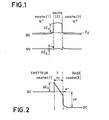
- Figure 1 shows schematically the equilibrium band diagram of a double heterojunction. This is formed by a layer 1 consisting of an N-type semiconductor material doped N> 5.10 17 e / cm 3 , and a layer 2 consisting of a high resistivity semiconductor having a larger band gap than the first semiconductor and the same mesh parameter. A layer 3 is formed from the same semiconductor material as the first and is also highly doped N> 5.10 17 e / cm 3 .
- the whole heterostructure is achievable by epitaxy, for example I epitaxy by molecular jets.
- BC, BV and E F respectively designate the conduction band, the valence band and the Fermi level.
- ⁇ E C and ⁇ E v are respectively the discontinuities in the conduction and valence bands at the interface.
- ⁇ E C constitutes a potential barrier for the electrons and AE v a barrier for the holes.
- layers 1 and 3 are N-type doped, only the electrons will be considered.
- Layers 1 and 2 constitute the emitter and layer 3 the base of the transistor according to the invention which will be described later.
- the basic electrical contact is of the ohmic type as is already known in bipolar transistors. It will be described later.
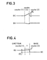
- FIG. 3 schematically represents the band diagram of a double heterojunction formed by a layer 1, a layer 4 and a layer 3.
- the layers 1 and 3 are identical to those already described on the occasion of FIG. 1.
- the layer 4 is of high resistivity. It differs from layer 2 in FIG. 1 in that its composition is variable so as to form a barrier of triangular potential at equilibrium, the highest part of the barrier being in contact with layer 3.
- FIG. 4 represents the conduction bands of this double heterojunction under positive polarization of the base 3.
- a polarization .V such as eV ⁇ E
- the electrons cross the barrier by thermionic effect.
- the electrons are therefore injected into the base with an energy at E, or very close to ⁇ E, because a tunnel effect assisted by thermionic effect is possible.
- the passage of current through a triangular barrier as described, has already been mentioned in the literature (CL Allyn, AC Gossard and W. Wiegmann, Appl. Phys. Letters 36, no.5, 373 (1981)), however its use in a transistor structure has not been envisaged.
- the data in the literature show that the current injected into the base follows an almost exponential law as a function of V.
- ⁇ E 1 the height of the potential barrier to the emitter, whatever the structure considered.
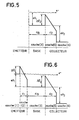
- the collector consists of two layers 5 and 6 forming with the layer 3 a heterojunction presenting a potential barrier AE 2 , in such a way that the layer 5 of high resistivity is in contact with the base 3 and that the potential barrier of height ⁇ E 2 that constitutes the layer 5 relative to the layers 3 and 6 is sufficiently high and / or of thickness d 2 sufficiently large so that a tunnel current between the base 3 and the layer 6 is negligible under a given voltage.
- the doping of layer 6 is greater than 5.10 17 e / cm 3 .
- FIG. 5 represents the strip diagram of such a base-collector structure under V 2 polarization between base and collector.
- the emitter is represented in the form of a junction from which hot electrons are injected into the base.
- the energy of the injected electrons is eV 1 . If eV 1 > ⁇ E2 and the thickness d B of the base is small enough for the ballistic path of the electrons to be possible through the base, these electrons can cross the barrier AE 2 .
- the term ballistics is taken here in the most general sense, including the overspeed effect. In other words, even if the electrons lose a certain amount of energy by impact, they can still cross the barrier ⁇ E 2 provided that the kinetic energy lost is less than eV 1 -A E 2 .
- the electrons also cross layer 5 by ballistic effect, otherwise their speed decreases in this zone to reach the speed limit v stat. . It is remarkable that the field in the base is very weak; consequently, during the crossing of the base, the electrons do not acquire additional speed; on the other hand, they can lose some as it was specified above.
- barrier heights polarization and thickness voltages of epitaxial layers
- ⁇ E 2 and d 2 must be as large as possible.
- d 2 the electrons are not in the ballistic path. Their speed is limited to v stat. .
- the charging time of the collector is then higher than in the case where d 2 is low, which reduces the cut-off frequency of the transistor.
- the upper limit of d 2 can be approximately 1 / ⁇ m.
- the lower limit of d 2 depends on the value of ⁇ E 2 .
- this dependence follows the law of d 2 ⁇ E 2 3/2 , for a given applied voltage and a given tunnel leakage current.
- d E 2 ⁇ 1 eV because of the choice of heterojunction couples
- d 2 must be greater than 400 A.
- the lower limit of ⁇ E 2 is conditioned by the tunnel effect assisted by thermionic effect.
- ⁇ E 2 > 0.2 eV must be used.
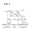
- FIG. 6 represents the band diagram of the emitter, base, collector under polarizations assembly, the emitter being constituted by layers 1 and 2 (tunnel effect).
- Figure 7 shows the case where the transmitter is consisting of layers 1 and 4 (thermionic effect).
- the following table specifies the different semiconductor materials that can be used. They are divided into three groups.
- the semiconductors of layers 1, 3 and 6 are determined.
- the second column lists the semiconductors of layers 2 and 5.
- the third column lists the semiconductors of layer 4. It is understood that layer 4 with variable composition can be used in place of layer 2 with constant composition, that the semiconductors 2 and 5 can be different in chemical composition, and that each material in the third column can be associated with any material in the second column corresponding to layer 5.
- FIGS. 8 to 13 schematically represent different variants of the transistor, according to the invention, with the emitter, base and collector electrical contacts.
- the epitaxy substrate is heavily N + doped.
- On this substrate are deposited, for example by molecular beam epitaxy, successively layers 1, 2 or 4, 3, 5 and 6.
- a mesa is released in layers 5 and 6 of collector up to the base layer 3 in order to deposit the ohmic base contact 9 there.
- the ohmic contact 7 of the emitter is deposited on the free face of the substrate, possibly thinned, to reduce the parasitic resistances, while the contact 8 of the collector is deposited on the layer 6.
- FIG. 9 represents, in very simplified schematic section, a first variant of a transistor according to the invention.
- the order of epitaxy of the layers is reversed, so that the collector is on the substrate, layers 5 and 6 being buried, while the emitter (layers 1 and 2 or 4 ) is on the free access side of the transistor. Only the base layer 3 and its metallization 9 remain in the same position as in the structure of the previous figure.
- FIG. 10 represents the adaptation of the structure of FIG. 8 in the case where the substrate is no longer of the N + type, that is to say conductive, but is of high resistivity, of the semi-insulating type.
- the order of epitaxy of the layers being the same as in the case of the basic structure of FIG. 8, it is no longer possible to make contact with the emitter 7 on the free face of the substrate, since the latter is semi-insulating. This is why a second mesa is made, up to layer 1, on which a metallization 7 is deposited, the base contact 9 being, as in the other cases, obtained after a mesa until layer 3.
- FIG. 11 represents the adaptation of the first variant of FIG. 9 to the case where the substrate is no longer of the N + type, but of the semi-insulating type.
- the order of epitaxy of the layers is therefore inverted there, but in this case, it is the collector contact 8 which is deposited on the layer 6, made accessible by etching a second mesa.
- FIG. 12 represents an improvement to the transistor according to the invention, applicable to the various variants described, although the structure shown is that of FIG. 10, without however being limiting.
- an area 10 made resistive by implantation, of H + ions for example is produced under the metallization 9 of the base.
- Zone 10, or box has a sufficient depth to reach the substrate.
Landscapes
- Bipolar Transistors (AREA)
Applications Claiming Priority (2)
| Application Number | Priority Date | Filing Date | Title |
|---|---|---|---|
| FR8112613A FR2508707A1 (fr) | 1981-06-26 | 1981-06-26 | Transistor balistique a multiples heterojonctions |
| FR8112613 | 1981-06-26 |
Publications (1)
| Publication Number | Publication Date |
|---|---|
| EP0070211A1 true EP0070211A1 (fr) | 1983-01-19 |
Family
ID=9259917
Family Applications (1)
| Application Number | Title | Priority Date | Filing Date |
|---|---|---|---|
| EP82401122A Withdrawn EP0070211A1 (fr) | 1981-06-26 | 1982-06-18 | Transistor balistique à multiples hétérojonctions |
Country Status (3)
| Country | Link |
|---|---|
| EP (1) | EP0070211A1 (OSRAM) |
| JP (1) | JPS589371A (OSRAM) |
| FR (1) | FR2508707A1 (OSRAM) |
Cited By (7)
| Publication number | Priority date | Publication date | Assignee | Title |
|---|---|---|---|---|
| EP0238406A3 (en) * | 1986-03-13 | 1987-11-19 | Fujitsu Limited | Heterojunction semiconductor device |
| EP0177374A3 (en) * | 1984-08-30 | 1987-11-25 | Fujitsu Limited | High-speed semiconductor device |
| US4958208A (en) * | 1987-08-12 | 1990-09-18 | Nec Corporation | Bipolar transistor with abrupt potential discontinuity in collector region |
| US5045296A (en) * | 1989-10-30 | 1991-09-03 | Fmc Corporation | Sodium carbonate perhydrate process |
| EP0662720A3 (en) * | 1994-01-07 | 1995-08-30 | Texas Instruments Inc | Tunnel effect hot electron transistor. |
| WO2005109519A1 (en) * | 2004-05-01 | 2005-11-17 | Cristopher Croft Jones | Charge carrier flow apparatus and methods |
| KR101235760B1 (ko) * | 2010-12-27 | 2013-02-28 | 재단법인 포항산업과학연구원 | 스틸 커튼월 장착구조 |
Families Citing this family (9)
| Publication number | Priority date | Publication date | Assignee | Title |
|---|---|---|---|---|
| JPS61121359A (ja) * | 1984-11-19 | 1986-06-09 | Fujitsu Ltd | 高速半導体装置の製造方法 |
| JPH0680675B2 (ja) * | 1984-03-06 | 1994-10-12 | 富士通株式会社 | 半導体装置の製造方法 |
| JPS61158172A (ja) * | 1984-12-29 | 1986-07-17 | Fujitsu Ltd | 高速半導体装置 |
| JPS61226961A (ja) * | 1985-04-01 | 1986-10-08 | Fujitsu Ltd | 高速半導体装置 |
| JPS624366A (ja) * | 1985-07-01 | 1987-01-10 | Fujitsu Ltd | ホツトエレクトロントランジスタ |
| JPS624365A (ja) * | 1985-07-01 | 1987-01-10 | Fujitsu Ltd | 半導体装置 |
| JPS63310167A (ja) * | 1987-06-12 | 1988-12-19 | Agency Of Ind Science & Technol | 半導体装置 |
| CA2072173C (en) * | 1991-06-24 | 2002-06-04 | Takayoshi Imoto | Lining material for pipe lines and a process for providing pipe lines therewith |
| JP2558383Y2 (ja) * | 1992-06-19 | 1997-12-24 | 三菱マテリアル株式会社 | サーミスタセンサ |
Citations (2)
| Publication number | Priority date | Publication date | Assignee | Title |
|---|---|---|---|---|
| FR2394174A1 (fr) * | 1977-06-09 | 1979-01-05 | Ibm | Dispositif a semi-conducteur du type transistor a heterojonctions a grande vitesse |
| EP0033876A2 (en) * | 1980-02-04 | 1981-08-19 | International Business Machines Corporation | Three-terminal semiconductor device |
-
1981
- 1981-06-26 FR FR8112613A patent/FR2508707A1/fr active Granted
-
1982
- 1982-06-18 EP EP82401122A patent/EP0070211A1/fr not_active Withdrawn
- 1982-06-26 JP JP57110561A patent/JPS589371A/ja active Pending
Patent Citations (2)
| Publication number | Priority date | Publication date | Assignee | Title |
|---|---|---|---|---|
| FR2394174A1 (fr) * | 1977-06-09 | 1979-01-05 | Ibm | Dispositif a semi-conducteur du type transistor a heterojonctions a grande vitesse |
| EP0033876A2 (en) * | 1980-02-04 | 1981-08-19 | International Business Machines Corporation | Three-terminal semiconductor device |
Cited By (8)
| Publication number | Priority date | Publication date | Assignee | Title |
|---|---|---|---|---|
| EP0177374A3 (en) * | 1984-08-30 | 1987-11-25 | Fujitsu Limited | High-speed semiconductor device |
| EP0238406A3 (en) * | 1986-03-13 | 1987-11-19 | Fujitsu Limited | Heterojunction semiconductor device |
| US5543749A (en) * | 1986-03-13 | 1996-08-06 | Fujitsu Limited | Resonant tunneling transistor |
| US4958208A (en) * | 1987-08-12 | 1990-09-18 | Nec Corporation | Bipolar transistor with abrupt potential discontinuity in collector region |
| US5045296A (en) * | 1989-10-30 | 1991-09-03 | Fmc Corporation | Sodium carbonate perhydrate process |
| EP0662720A3 (en) * | 1994-01-07 | 1995-08-30 | Texas Instruments Inc | Tunnel effect hot electron transistor. |
| WO2005109519A1 (en) * | 2004-05-01 | 2005-11-17 | Cristopher Croft Jones | Charge carrier flow apparatus and methods |
| KR101235760B1 (ko) * | 2010-12-27 | 2013-02-28 | 재단법인 포항산업과학연구원 | 스틸 커튼월 장착구조 |
Also Published As
| Publication number | Publication date |
|---|---|
| FR2508707B1 (OSRAM) | 1984-10-12 |
| JPS589371A (ja) | 1983-01-19 |
| FR2508707A1 (fr) | 1982-12-31 |
Similar Documents
| Publication | Publication Date | Title |
|---|---|---|
| EP0017531B1 (fr) | Transistor à effet de champ à fréquence de coupure élevée et son procédé de réalisation | |
| EP0070211A1 (fr) | Transistor balistique à multiples hétérojonctions | |
| EP0084393B1 (fr) | Dispositif semiconducteur du genre transistor à hétérojonction(s) | |
| US4835581A (en) | Electron gas hole gas tunneling transistor device | |
| EP3203526B1 (fr) | Transistor à hétérojonction à confinement de gaz d'électrons amélioré | |
| EP0236189B1 (fr) | Structure semi-conductrice monolithique d'un transistor bipolaire à hétérojonction et d'un laser | |
| FR2600821A1 (fr) | Dispositif semi-conducteur a heterojonction et double canal, son application a un transistor a effet de champ, et son application a un dispositif de transductance negative | |
| FR2586862A1 (fr) | Dispositif a semiconducteur en particulier du type mosfet. | |
| FR2517888A1 (fr) | Dispositif a semi-conducteur comportant une structure de grille associee a une jonction de faible profondeur | |
| US4825265A (en) | Transistor | |
| EP1243029B1 (fr) | Transistor bipolaire à hétérojonction collecteur en haut et procédé de réalisation | |
| Mehta et al. | Photoconductive gain greater than unity in CdSe films with Schottky barriers at the contacts | |
| EP0051504B1 (fr) | Transistors à effet de champ à grille ultra courte | |
| FR2568410A1 (fr) | Transistor statique a induction et son circuit integre | |
| FR2694449A1 (fr) | Composant électronique multifonctions, notamment élément à résistance dynamique négative, et procédé de fabrication correspondant. | |
| EP0050064B1 (fr) | Transistor à effet de champ à fréquence de coupure élevée | |
| EP0522952B1 (fr) | Transistor à effet de champ, à couches minces de barrière et couche mince dopée | |
| FR2745421A1 (fr) | Mesfet du type enrichissement | |
| FR2496990A1 (fr) | Transistor a effet de champ a barriere schottky | |
| FR2489045A1 (fr) | Transistor a effet de champ gaas a memoire non volatile | |
| FR2497603A1 (fr) | Transistor a faible temps de commutation, de type normalement bloquant | |
| FR2569056A1 (fr) | Transistor a induction statique du type a injection par effet tunnel et circuit integre comprenant un tel transistor | |
| EP3826072A1 (fr) | Transistor a gaz d'electrons, dispositif monobloc comportant au moins deux transistors en cascode et procedes de fabrication associes | |
| EP0083531B1 (fr) | Dispositif unipolaire à transfert d'électrons du type diode gunn | |
| EP0027761A1 (fr) | Dispositif semiconducteur à effet de champ pour hautes fréquences et transistor utilisant un tel dispositif semiconducteur |
Legal Events
| Date | Code | Title | Description |
|---|---|---|---|
| PUAI | Public reference made under article 153(3) epc to a published international application that has entered the european phase |
Free format text: ORIGINAL CODE: 0009012 |
|
| AK | Designated contracting states |
Designated state(s): DE GB IT NL |
|
| 17P | Request for examination filed |
Effective date: 19830127 |
|
| STAA | Information on the status of an ep patent application or granted ep patent |
Free format text: STATUS: THE APPLICATION IS DEEMED TO BE WITHDRAWN |
|
| 18D | Application deemed to be withdrawn |
Effective date: 19841231 |
|
| RIN1 | Information on inventor provided before grant (corrected) |
Inventor name: ETIENNE, PATRICK Inventor name: NUYEN, TRONG LINH Inventor name: DELAGEBEAUDEUF, DANIEL |