EP0068488B1 - Resist and process for forming resist pattern - Google Patents
Resist and process for forming resist pattern Download PDFInfo
- Publication number
- EP0068488B1 EP0068488B1 EP82105737A EP82105737A EP0068488B1 EP 0068488 B1 EP0068488 B1 EP 0068488B1 EP 82105737 A EP82105737 A EP 82105737A EP 82105737 A EP82105737 A EP 82105737A EP 0068488 B1 EP0068488 B1 EP 0068488B1
- Authority
- EP
- European Patent Office
- Prior art keywords
- resist
- thiocarbonyl fluoride
- polymer
- resist film
- thiocarbonyl
- Prior art date
- Legal status (The legal status is an assumption and is not a legal conclusion. Google has not performed a legal analysis and makes no representation as to the accuracy of the status listed.)
- Expired
Links
- 238000000034 method Methods 0.000 title claims description 9
- ZWEHNKRNPOVVGH-UHFFFAOYSA-N 2-Butanone Chemical compound CCC(C)=O ZWEHNKRNPOVVGH-UHFFFAOYSA-N 0.000 claims description 21
- -1 poly(thiocarbonyl fluoride) Polymers 0.000 claims description 21
- 229920000642 polymer Polymers 0.000 claims description 19
- 239000000758 substrate Substances 0.000 claims description 17
- FOCAHLGSDWHSAH-UHFFFAOYSA-N difluoromethanethione Chemical compound FC(F)=S FOCAHLGSDWHSAH-UHFFFAOYSA-N 0.000 claims description 15
- KFZMGEQAYNKOFK-UHFFFAOYSA-N Isopropanol Chemical compound CC(C)O KFZMGEQAYNKOFK-UHFFFAOYSA-N 0.000 claims description 10
- 230000005865 ionizing radiation Effects 0.000 claims description 10
- 239000003960 organic solvent Substances 0.000 claims description 9
- 229920001577 copolymer Polymers 0.000 claims description 8
- 238000010894 electron beam technology Methods 0.000 claims description 8
- PXGOKWXKJXAPGV-UHFFFAOYSA-N Fluorine Chemical compound FF PXGOKWXKJXAPGV-UHFFFAOYSA-N 0.000 claims description 6
- 239000002904 solvent Substances 0.000 claims description 6
- NTIZESTWPVYFNL-UHFFFAOYSA-N Methyl isobutyl ketone Chemical compound CC(C)CC(C)=O NTIZESTWPVYFNL-UHFFFAOYSA-N 0.000 claims description 5
- UIHCLUNTQKBZGK-UHFFFAOYSA-N Methyl isobutyl ketone Natural products CCC(C)C(C)=O UIHCLUNTQKBZGK-UHFFFAOYSA-N 0.000 claims description 5
- 150000001875 compounds Chemical class 0.000 claims description 5
- 229910052731 fluorine Inorganic materials 0.000 claims description 4
- 239000011737 fluorine Substances 0.000 claims description 4
- 230000001678 irradiating effect Effects 0.000 claims description 4
- 239000000203 mixture Substances 0.000 claims description 3
- LFQSCWFLJHTTHZ-UHFFFAOYSA-N Ethanol Chemical compound CCO LFQSCWFLJHTTHZ-UHFFFAOYSA-N 0.000 description 9
- 230000035945 sensitivity Effects 0.000 description 9
- HEDRZPFGACZZDS-UHFFFAOYSA-N Chloroform Chemical compound ClC(Cl)Cl HEDRZPFGACZZDS-UHFFFAOYSA-N 0.000 description 8
- 239000012046 mixed solvent Substances 0.000 description 6
- VZGDMQKNWNREIO-UHFFFAOYSA-N tetrachloromethane Chemical compound ClC(Cl)(Cl)Cl VZGDMQKNWNREIO-UHFFFAOYSA-N 0.000 description 6
- VYPSYNLAJGMNEJ-UHFFFAOYSA-N Silicium dioxide Chemical compound O=[Si]=O VYPSYNLAJGMNEJ-UHFFFAOYSA-N 0.000 description 4
- XUIMIQQOPSSXEZ-UHFFFAOYSA-N Silicon Chemical compound [Si] XUIMIQQOPSSXEZ-UHFFFAOYSA-N 0.000 description 4
- 229910052710 silicon Inorganic materials 0.000 description 4
- 239000010703 silicon Substances 0.000 description 4
- AJDIZQLSFPQPEY-UHFFFAOYSA-N 1,1,2-Trichlorotrifluoroethane Chemical compound FC(F)(Cl)C(F)(Cl)Cl AJDIZQLSFPQPEY-UHFFFAOYSA-N 0.000 description 3
- 239000000463 material Substances 0.000 description 3
- 238000000059 patterning Methods 0.000 description 3
- 238000002791 soaking Methods 0.000 description 3
- BFKJFAAPBSQJPD-UHFFFAOYSA-N tetrafluoroethene Chemical group FC(F)=C(F)F BFKJFAAPBSQJPD-UHFFFAOYSA-N 0.000 description 3
- 229910052581 Si3N4 Inorganic materials 0.000 description 2
- 238000010438 heat treatment Methods 0.000 description 2
- 239000004065 semiconductor Substances 0.000 description 2
- 235000012239 silicon dioxide Nutrition 0.000 description 2
- 239000000377 silicon dioxide Substances 0.000 description 2
- HQVNEWCFYHHQES-UHFFFAOYSA-N silicon nitride Chemical compound N12[Si]34N5[Si]62N3[Si]51N64 HQVNEWCFYHHQES-UHFFFAOYSA-N 0.000 description 2
- BQCIDUSAKPWEOX-UHFFFAOYSA-N 1,1-Difluoroethene Chemical compound FC(F)=C BQCIDUSAKPWEOX-UHFFFAOYSA-N 0.000 description 1
- VYZAMTAEIAYCRO-UHFFFAOYSA-N Chromium Chemical compound [Cr] VYZAMTAEIAYCRO-UHFFFAOYSA-N 0.000 description 1
- YZCKVEUIGOORGS-OUBTZVSYSA-N Deuterium Chemical compound [2H] YZCKVEUIGOORGS-OUBTZVSYSA-N 0.000 description 1
- UFHFLCQGNIYNRP-UHFFFAOYSA-N Hydrogen Chemical compound [H][H] UFHFLCQGNIYNRP-UHFFFAOYSA-N 0.000 description 1
- CERQOIWHTDAKMF-UHFFFAOYSA-M Methacrylate Chemical compound CC(=C)C([O-])=O CERQOIWHTDAKMF-UHFFFAOYSA-M 0.000 description 1
- NINIDFKCEFEMDL-UHFFFAOYSA-N Sulfur Chemical compound [S] NINIDFKCEFEMDL-UHFFFAOYSA-N 0.000 description 1
- 230000001133 acceleration Effects 0.000 description 1
- 238000012644 addition polymerization Methods 0.000 description 1
- 238000007605 air drying Methods 0.000 description 1
- 239000011692 calcium ascorbate Substances 0.000 description 1
- 238000006243 chemical reaction Methods 0.000 description 1
- 229910052804 chromium Inorganic materials 0.000 description 1
- 239000011651 chromium Substances 0.000 description 1
- 239000011248 coating agent Substances 0.000 description 1
- 238000000576 coating method Methods 0.000 description 1
- 230000007547 defect Effects 0.000 description 1
- 229910052805 deuterium Inorganic materials 0.000 description 1
- 238000001035 drying Methods 0.000 description 1
- 238000001704 evaporation Methods 0.000 description 1
- XUCNUKMRBVNAPB-UHFFFAOYSA-N fluoroethene Chemical compound FC=C XUCNUKMRBVNAPB-UHFFFAOYSA-N 0.000 description 1
- 229920002313 fluoropolymer Polymers 0.000 description 1
- 239000011521 glass Substances 0.000 description 1
- HCDGVLDPFQMKDK-UHFFFAOYSA-N hexafluoropropylene Chemical compound FC(F)=C(F)C(F)(F)F HCDGVLDPFQMKDK-UHFFFAOYSA-N 0.000 description 1
- 229920001519 homopolymer Polymers 0.000 description 1
- 229910052739 hydrogen Inorganic materials 0.000 description 1
- 239000001257 hydrogen Substances 0.000 description 1
- 230000010354 integration Effects 0.000 description 1
- 238000002156 mixing Methods 0.000 description 1
- 229920003229 poly(methyl methacrylate) Polymers 0.000 description 1
- 238000006116 polymerization reaction Methods 0.000 description 1
- 230000000379 polymerizing effect Effects 0.000 description 1
- 239000004926 polymethyl methacrylate Substances 0.000 description 1
- 238000002360 preparation method Methods 0.000 description 1
- CAEWJEXPFKNBQL-UHFFFAOYSA-N prop-2-enyl carbonochloridate Chemical compound ClC(=O)OCC=C CAEWJEXPFKNBQL-UHFFFAOYSA-N 0.000 description 1
- 239000002994 raw material Substances 0.000 description 1
- 229910052717 sulfur Inorganic materials 0.000 description 1
- 239000011593 sulfur Substances 0.000 description 1
- 230000004304 visual acuity Effects 0.000 description 1
Images
Classifications
-
- G—PHYSICS
- G03—PHOTOGRAPHY; CINEMATOGRAPHY; ANALOGOUS TECHNIQUES USING WAVES OTHER THAN OPTICAL WAVES; ELECTROGRAPHY; HOLOGRAPHY
- G03F—PHOTOMECHANICAL PRODUCTION OF TEXTURED OR PATTERNED SURFACES, e.g. FOR PRINTING, FOR PROCESSING OF SEMICONDUCTOR DEVICES; MATERIALS THEREFOR; ORIGINALS THEREFOR; APPARATUS SPECIALLY ADAPTED THEREFOR
- G03F7/00—Photomechanical, e.g. photolithographic, production of textured or patterned surfaces, e.g. printing surfaces; Materials therefor, e.g. comprising photoresists; Apparatus specially adapted therefor
- G03F7/004—Photosensitive materials
- G03F7/039—Macromolecular compounds which are photodegradable, e.g. positive electron resists
-
- Y—GENERAL TAGGING OF NEW TECHNOLOGICAL DEVELOPMENTS; GENERAL TAGGING OF CROSS-SECTIONAL TECHNOLOGIES SPANNING OVER SEVERAL SECTIONS OF THE IPC; TECHNICAL SUBJECTS COVERED BY FORMER USPC CROSS-REFERENCE ART COLLECTIONS [XRACs] AND DIGESTS
- Y10—TECHNICAL SUBJECTS COVERED BY FORMER USPC
- Y10T—TECHNICAL SUBJECTS COVERED BY FORMER US CLASSIFICATION
- Y10T428/00—Stock material or miscellaneous articles
- Y10T428/24—Structurally defined web or sheet [e.g., overall dimension, etc.]
- Y10T428/24273—Structurally defined web or sheet [e.g., overall dimension, etc.] including aperture
- Y10T428/24298—Noncircular aperture [e.g., slit, diamond, rectangular, etc.]
- Y10T428/24306—Diamond or hexagonal
Definitions
- the present invention relates to a resist and a process for forming a resist pattern. More particularly, the invention relates to a poly(thiocarbonyl fluoride) resist which is sensitive to an ionizing radiation and a process for forming a resist pattern by forming the resist film on a substrate, irradiating the film with an ionizing radiation and developing with an organic solvent.
- Polymethyl methacrylate is put to practical use as a positive type resist.
- the sensitivity of this resist is about 1 x 1 0-4 coulomb/cm 2 and the y value showing resolution is about 3.3.
- a poly-(fluoroalkyl methacrylate) is also known as a resist material having excellent sensitivity and y value from Japanese Patent Publication No. 24088/1980, and some poly(fluoroalkyl methacrylate) has a sensitivity of 4x10-' coulomb/cm 2 .
- the y value of the poly(fluoroalkyl methacrylate) is within the range of from about 4.5 to about 10.
- the polymers of this kind have the defect, and it is reported in Japanese Patent Publication No. 30613/1980 that the polymers are poor in adhesion to substrates such as silicon dioxide, silicon and silicon nitride and a developer often soaks into the interface between the resist and the substrate during the development to cause the resist film to peel off.
- a further object of the invention is to provide a resist capable of forming a fine resist pattern.
- Another object of the invention is to provide a process for forming a fine resist pattern.
- poly(thiocarbonyl fluoride) which has entirely different structure and properties from methacrylate polymers conventionally known as positive type resists, has a sensitivity and resolving power to an ionizing radiation which are comparable to those of the above-mentioned poly(fluoroalkyl methacrylate), and moreover it can provide a positive type resist having excellent adhesion to a substrate.
- a resist which comprises a thiocarbonyl fluoride polymer selected from the group consisting of poly(thiocarbonyl fluoride), copolymers of thiocarbonyl fluoride with ethylenically unsaturated compounds, and the thiocarbonyl fluoride homo- and co-polymers partially modifed with elemental fluorine.
- the present invention also provides a process for forming a resist pattern which comprises the steps of forming a resist film of a thiocarbonyl fluoride polymer on a substrate, irradiating the resist film with an ionizing radiation and developing it with an organic solvent.
- Poly(thiocarbonyl fluoride) used in the present invention is a known polymer consisting of recurring units of the formula (I): and the polymer having a molecular weight of 10,000 to 1,500,000 is preferred.
- copolymers of thiocarbonyl fluorides with other ethylenically unsaturated compounds capable of addition polymerization examples of the ethylenically unsaturated compounds are tetrafluoroethylene, vinyl fluoride, vinylidene fluoride, hexafluoro- propene, trifluoroethylene, chlorotrifluoroethylene, propene and allyl chloroformate.
- the above thiocarbonyl fluoride homopolymer and copolymers may be partially modifed with elemental fluorine, and such partially fluorinated polymers can also be employed in the present invention.
- Poly(thiocarbonyl fluoride) is prepared by polymerizing thiocarbonyl fluoride of the formula (II): as disclosed in detail in a report of W.J. Middleton et al, J. Polymer Sci., Part A, Vol. 3, 4115(1965).
- the above-mentioned thiocarbonyl fluoride polymer is soluble in organic solvents such as chloroform, carbon tetrachloride, 1,1,2-trifluoro-1,2,2-trichloroethane, methyl ethyl ketone and methyl isobutyl ketone.
- organic solvents such as chloroform, carbon tetrachloride, 1,1,2-trifluoro-1,2,2-trichloroethane, methyl ethyl ketone and methyl isobutyl ketone.
- a resist film can be formed from a solution of the polymer in these solvents.
- a resist film of a thiocarbonyl fluoride polymer of the present invention is formed by dissolving the polymer in an organic solvent such as chloroform, carbon tetrachloride or 1,1,2-trifluorotrichloroethane to give a solution, coating the solution on a substrate, for instance, with a spin coater, and evaporating the solvent by heating or air-drying.
- an organic solvent such as chloroform, carbon tetrachloride or 1,1,2-trifluorotrichloroethane
- the substrates to be used in the present invention are not particularly limited, and various kinds of substrates can be used, e.g. a glass plate masked with chromium, and a semiconductor film such as silicon, silicon dioxide or silicon nitride.
- the resist film of the invention can be delineated with an ionizing radiation such as electron beams, X-rays or deep ultraviolet rays.
- a resist pattern is formed by irradiating the resist film with an ionizing radiation according to a predetermined pattern, and developing it with an organic solvent.
- the resist film of the invention has a high sensitivity on the order of 10- 6 coulomb/cm 2 and an excellent resolution of y value from 1.0 to 3.3, and is useful high sensitive resist of positive type comparable to a poly(fluoroalkyl methacrylate) resist.
- Organic solvents used for development are not particularly limited, and for instance, mixture of a good solvent such as chloroform, carbon tetrachloride, 1,1,2-trifluoro-1,2,2-trichloroethane, methyl ethyl ketone or methyl isobutyl ketone and a poor solvent such as a lower alcohol as usable.
- a mixed solvent of methyl ethyl ketone and ethanol, especially in a ratio of 50:50 to 99:1 by volume, is preferably used as a developer.
- a mixed solvent of methyl isobutyl ketone and isopropanol especially in a ratio of 99:1 to 10:90 by volume, is preferably employed as a developer.
- the development time is suitably determined according to conditions such as degree of polymerization of the polymer, kind of ionizing radiation, kind of developer, mixing ratio of organic solvents and developing temperature. For instance, it is selected from 10 seconds to 30 minutes.
- a 8% by weight solution of poly(thiocarbonyl fluoride) having a number average molecluar weight of 350,000 was prepared by dissolving the polymer in chloroform, and was coated onto a silicon substrate by a spin coater over 60 seconds. The solvent was then evaporated by heating the coated substrate at 140°C for 30 minutes to form a resist film having a thickness of 0.25 ⁇ m.
- the electron beam delineation of the resist film was carried out by employing E-302 type electron beam delineation apparatus made by Kabushiki Kaisha Elionix, Japan. Electron beams (current: 1x10- 9 A, acceleration voltage: 20 kV) were irradiated to different portions 4.3x10- 4 cm 2 of the resist film for 0.08 second (1.87X10 -7 coulomb/cm 2 ) to 125 seconds (2.88x10 -4 coulomb/cm 2 ) to form a 32 pm line and space pattern.
- the irradiated resist film was then immersed in a mixed solvent of methyl ethyl ketone and ethanol in a volume ratio of 90:10 for 90 seconds to develop the resist pattern, and washed by immersing in isopropanol for 60 seconds.
- the thickness was measured by employing a Talystep (Rank Taylor Hobson, England).
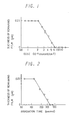
- Fig. 1 The relationship between the dose of electron beams (coulomb/cm 2 ) and the thickness of the remaining film (pm) is shown in Fig. 1. It is found from Fig. 1 that the sensitivity and y value of the resist are 6.3x10 -6 coulomb/cm 2 and 2.0, respectively.
- Example 1 The procedure of Example 1 was repeated except that a mixed solvent of methyl ethyl ketone and ethanol in a volume ratio of 95:5 was employed as a developer instead of the mixed solvent of methyl ethyl ketone and ethanol in a volume ratio of 90:10.
- the sensitivity was 3.70x10- 6 coulomb/cm 2 and the y value was 3.3.
- a resist film was formed on a silicon substrate in the same manner as in Example 1, and exposed to deep ultraviolet rays (wavelength: not less than 180 nm) form a deuterium hydrogen lamp (400 W, 1.5 A) 5 cm distant from the resist film for varied period of irradiation time (at 1 minute intervals from 1 to 8 minutes).
- the irradiated resist film was immersed in a mixed solvent of methyl isobutyl ketone and isopropanol (60:40 by volume) at 23°C for 90 seconds for development, immersed in isopropanol for 60 seconds to wash and then dried.
- Fig. 2 The relationship between the thickness of the remaining film and the irradiation time is shown in Fig. 2. It is found from Fig. 2 that the sensitivity and y value of the resist film are 0.060 J/cm 2 and 2.0, respectively.
- the resist film had an excellent adhesion to the substrate.
Landscapes
- Physics & Mathematics (AREA)
- Spectroscopy & Molecular Physics (AREA)
- General Physics & Mathematics (AREA)
- Photosensitive Polymer And Photoresist Processing (AREA)
- Materials For Photolithography (AREA)
- Exposure And Positioning Against Photoresist Photosensitive Materials (AREA)
Applications Claiming Priority (2)
| Application Number | Priority Date | Filing Date | Title |
|---|---|---|---|
| JP56102726A JPS584137A (ja) | 1981-06-30 | 1981-06-30 | レジストおよび微細レジストパタ−ンの形成方法 |
| JP102726/81 | 1981-06-30 |
Publications (2)
| Publication Number | Publication Date |
|---|---|
| EP0068488A1 EP0068488A1 (en) | 1983-01-05 |
| EP0068488B1 true EP0068488B1 (en) | 1985-06-12 |
Family
ID=14335260
Family Applications (1)
| Application Number | Title | Priority Date | Filing Date |
|---|---|---|---|
| EP82105737A Expired EP0068488B1 (en) | 1981-06-30 | 1982-06-28 | Resist and process for forming resist pattern |
Country Status (4)
| Country | Link |
|---|---|
| US (1) | US4656108A (enExample) |
| EP (1) | EP0068488B1 (enExample) |
| JP (1) | JPS584137A (enExample) |
| DE (1) | DE3264117D1 (enExample) |
Family Cites Families (4)
| Publication number | Priority date | Publication date | Assignee | Title |
|---|---|---|---|---|
| US2980695A (en) * | 1957-06-12 | 1961-04-18 | Du Pont | Polyfluoro-1, 3-dithietanes and their preparation |
| US3240765A (en) * | 1961-05-01 | 1966-03-15 | Du Pont | Thiocarbonyl fluorides and their polymers |
| JPS5290269A (en) * | 1976-01-23 | 1977-07-29 | Nippon Telegr & Teleph Corp <Ntt> | Forming method for fine resist patterns |
| US4125671A (en) * | 1977-05-06 | 1978-11-14 | Thiokol Corporation | Acrylated dithiocarbamyl esters |
-
1981
- 1981-06-30 JP JP56102726A patent/JPS584137A/ja active Granted
-
1982
- 1982-06-28 DE DE8282105737T patent/DE3264117D1/de not_active Expired
- 1982-06-28 EP EP82105737A patent/EP0068488B1/en not_active Expired
-
1985
- 1985-06-20 US US06/746,932 patent/US4656108A/en not_active Expired - Fee Related
Non-Patent Citations (1)
| Title |
|---|
| NONE * |
Also Published As
| Publication number | Publication date |
|---|---|
| JPS6410059B2 (enExample) | 1989-02-21 |
| EP0068488A1 (en) | 1983-01-05 |
| JPS584137A (ja) | 1983-01-11 |
| US4656108A (en) | 1987-04-07 |
| DE3264117D1 (en) | 1985-07-18 |
Similar Documents
| Publication | Publication Date | Title |
|---|---|---|
| KR900002364B1 (ko) | 패턴 형성재의 제조방법 | |
| EP0090089B1 (en) | Resist material and process for forming fine resist pattern | |
| US4259407A (en) | Radiation-sensitive positive resist | |
| US4357369A (en) | Method of plasma etching a substrate | |
| JPS6048022B2 (ja) | 電子感応レジスト | |
| EP0067066B2 (en) | Dry-developing resist composition | |
| US4518675A (en) | Stripper for radiosensitive resist | |
| US3987215A (en) | Resist mask formation process | |
| JPS64689B2 (enExample) | ||
| US4096290A (en) | Resist mask formation process with haloalkyl methacrylate copolymers | |
| US4301231A (en) | Negative resist for high energy radiation | |
| KR940002549B1 (ko) | 레지스트 조성물과 패턴 형성방법 | |
| EP0424182A2 (en) | Process for formation of resist patterns | |
| US4346163A (en) | Resist for use in forming a positive pattern with a radiation and process for forming a positive pattern with radiation | |
| EP0025633A1 (en) | A method of applying a layer in accordance with a pattern on a substrate | |
| EP0068488B1 (en) | Resist and process for forming resist pattern | |
| US4237208A (en) | Silane electron beam resists | |
| EP0030107B1 (en) | Process for forming resist pattern | |
| US4302529A (en) | Process for developing a positive electron resist | |
| EP0064864B1 (en) | Method of making sensitive positive electron beam resists | |
| JPS5953837A (ja) | パタン形成材料およびパタン形成法 | |
| US4581318A (en) | N-alkynyl polyvinylpyridinium resists having electron and deep U.V. sensitivity | |
| US4520097A (en) | Negative-type resist sensitive to ionizing radiation | |
| US4677048A (en) | Process of using N-alkynyl polyvinylpyridinium resists having electron and deep U.V. sensitivity | |
| JPS6259950A (ja) | 電離放射線感応ポジ型レジスト |
Legal Events
| Date | Code | Title | Description |
|---|---|---|---|
| PUAI | Public reference made under article 153(3) epc to a published international application that has entered the european phase |
Free format text: ORIGINAL CODE: 0009012 |
|
| AK | Designated contracting states |
Designated state(s): DE FR GB NL |
|
| 17P | Request for examination filed |
Effective date: 19830625 |
|
| GRAA | (expected) grant |
Free format text: ORIGINAL CODE: 0009210 |
|
| AK | Designated contracting states |
Designated state(s): DE FR GB NL |
|
| REF | Corresponds to: |
Ref document number: 3264117 Country of ref document: DE Date of ref document: 19850718 |
|
| ET | Fr: translation filed | ||
| PLBE | No opposition filed within time limit |
Free format text: ORIGINAL CODE: 0009261 |
|
| STAA | Information on the status of an ep patent application or granted ep patent |
Free format text: STATUS: NO OPPOSITION FILED WITHIN TIME LIMIT |
|
| 26N | No opposition filed | ||
| PGFP | Annual fee paid to national office [announced via postgrant information from national office to epo] |
Ref country code: GB Payment date: 19910614 Year of fee payment: 10 |
|
| PGFP | Annual fee paid to national office [announced via postgrant information from national office to epo] |
Ref country code: FR Payment date: 19910619 Year of fee payment: 10 |
|
| PGFP | Annual fee paid to national office [announced via postgrant information from national office to epo] |
Ref country code: NL Payment date: 19910630 Year of fee payment: 10 |
|
| PGFP | Annual fee paid to national office [announced via postgrant information from national office to epo] |
Ref country code: DE Payment date: 19910723 Year of fee payment: 10 |
|
| PG25 | Lapsed in a contracting state [announced via postgrant information from national office to epo] |
Ref country code: GB Effective date: 19920628 |
|
| PG25 | Lapsed in a contracting state [announced via postgrant information from national office to epo] |
Ref country code: NL Effective date: 19930101 |
|
| NLV4 | Nl: lapsed or anulled due to non-payment of the annual fee | ||
| GBPC | Gb: european patent ceased through non-payment of renewal fee |
Effective date: 19920628 |
|
| PG25 | Lapsed in a contracting state [announced via postgrant information from national office to epo] |
Ref country code: FR Effective date: 19930226 |
|
| PG25 | Lapsed in a contracting state [announced via postgrant information from national office to epo] |
Ref country code: DE Effective date: 19930302 |
|
| REG | Reference to a national code |
Ref country code: FR Ref legal event code: ST |