EP0054412A2 - Verfahren und Vorrichtung zum Behandeln einer negativen Photoresistschicht - Google Patents
Verfahren und Vorrichtung zum Behandeln einer negativen Photoresistschicht Download PDFInfo
- Publication number
- EP0054412A2 EP0054412A2 EP81305824A EP81305824A EP0054412A2 EP 0054412 A2 EP0054412 A2 EP 0054412A2 EP 81305824 A EP81305824 A EP 81305824A EP 81305824 A EP81305824 A EP 81305824A EP 0054412 A2 EP0054412 A2 EP 0054412A2
- Authority
- EP
- European Patent Office
- Prior art keywords
- chamber
- exposure
- gas
- negative photoresist
- vacuum
- Prior art date
- Legal status (The legal status is an assumption and is not a legal conclusion. Google has not performed a legal analysis and makes no representation as to the accuracy of the status listed.)
- Granted
Links
Images


Classifications
-
- G—PHYSICS
- G03—PHOTOGRAPHY; CINEMATOGRAPHY; ANALOGOUS TECHNIQUES USING WAVES OTHER THAN OPTICAL WAVES; ELECTROGRAPHY; HOLOGRAPHY
- G03F—PHOTOMECHANICAL PRODUCTION OF TEXTURED OR PATTERNED SURFACES, e.g. FOR PRINTING, FOR PROCESSING OF SEMICONDUCTOR DEVICES; MATERIALS THEREFOR; ORIGINALS THEREFOR; APPARATUS SPECIALLY ADAPTED THEREFOR
- G03F7/00—Photomechanical, e.g. photolithographic, production of textured or patterned surfaces, e.g. printing surfaces; Materials therefor, e.g. comprising photoresists; Apparatus specially adapted therefor
- G03F7/26—Processing photosensitive materials; Apparatus therefor
- G03F7/38—Treatment before imagewise removal, e.g. prebaking
-
- G—PHYSICS
- G03—PHOTOGRAPHY; CINEMATOGRAPHY; ANALOGOUS TECHNIQUES USING WAVES OTHER THAN OPTICAL WAVES; ELECTROGRAPHY; HOLOGRAPHY
- G03F—PHOTOMECHANICAL PRODUCTION OF TEXTURED OR PATTERNED SURFACES, e.g. FOR PRINTING, FOR PROCESSING OF SEMICONDUCTOR DEVICES; MATERIALS THEREFOR; ORIGINALS THEREFOR; APPARATUS SPECIALLY ADAPTED THEREFOR
- G03F7/00—Photomechanical, e.g. photolithographic, production of textured or patterned surfaces, e.g. printing surfaces; Materials therefor, e.g. comprising photoresists; Apparatus specially adapted therefor
- G03F7/20—Exposure; Apparatus therefor
-
- Y—GENERAL TAGGING OF NEW TECHNOLOGICAL DEVELOPMENTS; GENERAL TAGGING OF CROSS-SECTIONAL TECHNOLOGIES SPANNING OVER SEVERAL SECTIONS OF THE IPC; TECHNICAL SUBJECTS COVERED BY FORMER USPC CROSS-REFERENCE ART COLLECTIONS [XRACs] AND DIGESTS
- Y10—TECHNICAL SUBJECTS COVERED BY FORMER USPC
- Y10S—TECHNICAL SUBJECTS COVERED BY FORMER USPC CROSS-REFERENCE ART COLLECTIONS [XRACs] AND DIGESTS
- Y10S430/00—Radiation imagery chemistry: process, composition, or product thereof
- Y10S430/167—X-ray
- Y10S430/168—X-ray exposure process
Definitions
- This invention relates to a method of and apparatus for processing negative photoresist.
- the exposure step involves a period of a duration in the range from 50 or 60 minutes to several hours, although very precise and fine patterns can be formed.
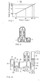
- FIG. 1 of the accompanying drawings is a graph illustrating the relationship between the width W or thickness T of a written pattern (indicated along the vertical axis in Figure 1) and the length of curing time t after exposure (indicated along the horizontal axis in Figure 1 , on a logarithmic scale).
- the apparatus according to that disclosed invention involves a technique for transferring articles irradiated by electron beams, ion beams, etc, in vacuum.
- a paragraph bridging pages 1 and 2 of the specification of this publication there appears a description which indicates that developments are being made to use electron beams and ion beams widely for treatment and processing of metals and other materials, for example dissolution, blowout, welding, heat treatment, sputtering, etching, ion implantation and the like.
- Japanese Patent Publication (unexamined) No.68622 of 1980 published on 23rd May 1980, discloses an invention entitled "Device for Exchanging Samples in an Apparatus for Electron Beam Pattern Writing."
- page 4 of the specification thereof is a description of a curing chamber which is kept in a. 1 .vacuum of the order of less than 10 -4 Torr.
- the curing chamber is independent of a chamber wherein samples are loaded and unloaded, and the object is to carry out curing of samples in vacuum in accordance with the claim of the specification.
- page 6 of the specification there appears a discription which indicates that when pattern writing is over, samples are cured in vacuum without ejection of the mask to the outside atmosphere.
- page 7 of the specification it is indicated that, for the purpose of improving exposure and stabilising the width of the lines of the pattern, curing in vacuum is necessary.
- vacuum of the order of higher than 1 x 10 -4 Torr
- the width of a line of a pattern increases. After lapse of a certain length of time, this tendency subsides , and when the photoresist is placed in a vacuum of lesser degree, or in the atmposphere, the polymerisation ceases.
- the curing is carried out which pattern writing is carried to the sample.
- the sample is taken out of the curing chamber, and while maintaining the chamber in vacuum, the sample is transferred to a next stage of the process.
- page 16 of the specification it is described that the device of the invention allows the maintenance of the high degree of vacuum required for the curing .
- a method of processing negative photoresist comprising exposing the negative photoresist to charged particle beams or soft X-ray beams in a vacuum, characterised in that, after such exposure, the negative photoresist is held in an atmosphere of non-oxidising gas before being exposed to the outside atmosphere.
- apparatus for processing a negative photoresist having an exposure chamber in which the negative photoresist is exposed to charged particle beams or soft X-ray beams in vacuum when the apparatus is in use, characterised in that the apparatus comprises a gas chamber for holding the negative photoresist, after exposure in the exposure chamber, in a non-oxidising gas in the gas chamber, before the negative photoresist is exposed to the outside atmosphere.
- a method embodying the present invention prescribes the keeping of a film of negative photoresist emulsion in an atmosphere of gas not containing oxygen, or containing only a small percentage of oxygen, after exposure of the photoresist to electron beams or the like. Apparatus is provided for carrying out such a method.
- the present invention offers a solution to the problem experienced in the conventional art by offering a method of keeping a substrate or wafer having negative photoresist emulsion thereon, that has been exposed to electron beams, for a predetermined length of time in an atmosphere of non-oxidising gas.
- the present invention offers an improved electron beam exposure apparatus which eliminates the curing effect as described above and in which a mechanism is provided for introducing, and for keeping for a predetermined length of time, wafers which have been exposed to electron beams in a chamber filled with non-oxidising gas.
- a film of negative photoresist emulsion on a substrate to be treated is exposed, for pattern writing , in vacuum, to charged particle beams or .soft X-ray beams, then the substrate coated with the photoresist film is transferred to , and kept in, a chamber having an atmosphere of non-oxidising, gas,. and is finally taken out of the chamber into the outside atmosphere.
- the non-oxidising gas may contain oxygen in an amount less than, or not more than,l% in volume terms.
- a further method embodying the present invention comprises the following steps : irradiating charged particle beams or soft X-ray beams onto a substrate coated with a film of negative photoresist emulsion, to be treated for pattern writing exposure , in vacuum; transferring the substrate in vacuum to a gas chamber connected to the chamber where exposure is carried out ; shutting off the exposure chamber from the gas chamber ; introducing non-oxidising gas into the gas chamber and maintaining the substrate in an atmosphere of non-oxidising gas ; and taking out the substrate from the atmosphere of non-oxidising gas to the outside atmosphere.
- Another method embodying the present invention comprises the, steps of : irradiating charged particle beams or soft X-ray beams onto a substrate coated with a film of negative photoresist emulsion to be greated for pattern writing exposure ; transferring the substrate in vacuum to a sub-chamber connected to the exposure chamber; shutting off the connection between the exposure chamber and the sub-chamber; introducing non-oxidising gas into the sub-chamber and maintaining the substrate in an atmosphere of non-oxidising gas; transferring the substrate in the atmosphere of non-oxidising gas to a gas chamber connected to the sub-chamber; and taking out the substrate from the gas chamber to the outside atmosphere.
- a gas chamber filled with non-oxidising gas is connected to an exposure chamber wherein charged particle beams are irradiated onto a film of negative photoresist on a substrate for pattern writing exposure, and the substrate, after exposure to processing is over in the exposure chamber, is kept in the atmosphere of non-oxidising gas in the gas chamber and then taken out to the outside atmosphere.
- a sub-chamber is interposed between'the exposure chamber and the gas chamber.
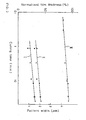
- irradiated electron beam dose in Coulomb per cm 2 is indicated along the horizontal axis and normalised film thickness, or ratio of thicknesses of the photoresist film before and after development (in %) is indicated along the vertical axis.
- the curves in Figure 2 illustrate that film thickness increases proportionately as dose (in C/cm 2 ) increases.
- Wafers were coated with negative photoresist emulsion, poly-diaryl-ortho-phthalate (PDOP) for example; the photoresist film was prebaked at 60°C for 20 minutes, and postbaked at 90°C for 20 minutes. Wafers were taken out of vacuum as follows: Soon after exposure without any curing time, and after curing times of 3 minutes, 10 minutes and 30 minutes, respectively.
- PDOP poly-diaryl-ortho-phthalate
- results relating to wafers with 0 minute curing time are marked with circles
- results relating to 3 minute curing time are marked with X marks
- results relating to 10 minute curing time are marked with triangular marks
- results relating to 30 minutes curing time are marked with square marks.
- the graph shows that normalised film thickness varies as to the amount of dose changes, and that it increases as the time for which the photoresist is left in vacuum after exposure to electron beams increases. It is understood that this phenomenon is due to curing or subsequent polymerisation which takes a certain length of time before it levels off.
- the mode of change of the illustrated normalised film thickness varies as the exposure system and negative photoresist emulsion are changed. However, with negative photoresist emulsion, the same trend is noted for all practical purposes.
- the width of a given pattern is proportionate to the normalised film thickness, and thinning in the width of a pattern makes it difficult to form fine patterns accurately.
- Negative photoresist (poly-diaryl-ortho-phthalate) initially 1.18 to 1.25 ⁇ m thick was prebaked at 60°C for 20 minutes. The emulsion was irradiated with an electron beam dosage of 3.5 x 10 -5 C/cm 2 at an energy of 20 KeV. Dark circles and dark squares indicate results obtained in vacuum, and plain circles and plain squares indicate results obtained in nitrogen atmosphere.
- the maximum volume of oxygen that can be contained in gas in which the negative photoresist emulsion is kept is 1%.
- a substrate to be treated which is coated with negative photoresist emulsion is exposed, and, without taking the substrate into the outside air, it is kept in nitrogen gas for a period in the range 30 minutes to 1 hour.
- a semiconductor substrate 2 placed in a stage chamber 1 of an apparatus for electron beam exposure is exposed to electron beams in vacuum. Exhaustion of air to keep the stage chamber 1 in vacuum is stopped, and nitrogen gas is introduced into the chamber 1.
- the substrate 2 is then transferred as indicated by an arrow in Figure 5 to a chamber 3 which has been filled with nitrogen gas.
- the substrate 2 is kept in chamber 3 for a period of from 30 minutes to 1 hour, and is subsequently .1 taken out into the outside air.
- the length of time during which the substrate 2 is kept in the nitrogen filled chamber 3 depends on the kind of negative photoresist emulsion and the type of exposure used..
- the apparatus of Figure 5 is as effective for forming high precision patterns on a semiconductor substrate as apparatus in which the substrate is kept in vacuum after exposure. It was confirmed that in the illustrated apparatus of Figure 5, rate of operation is improved considerably.
- a method in accordance with the present invention may alternatively be carried out in electron beam exposure apparatus as illustrated in Figure 6.
- the apparatus of Figure 6 comprises an exposure chamber 11, a loading chamber 12 and a store chamber 13 where substrates are temporarily held.
- the loading chamber 12 is provided with a pre-exhausting chamber 14, and the store chamber 13 with an unloading chamber 15.
- the pre-exhausting chamber 14 and the loading chamber 12 are connected by a gate valve 16 by which these chambers are either open to, or shut off from, one another.
- the loading chamber 12 and the exposure chamber 11 are similarly connected by a gate valve 17.
- the exposure chamber 11 and the store chamber 13 may be open to -,or shut off from, each other by a gate valve 18.
- the store chamber 13 and the unloading chamber 15 are connected by a gate valve 19.
- the gate valve 16 to the pre-exhausting chamber 14 and the gate valve 19 to the unloading chamber 15 are closed, and in the illustrated electron beam apparatus, air is exhausted from the loading chamber 12, exposure chamber 11 and the store chamber 13 to keep these chambers in a high degree of vacuum.
- the unloading chamber 15 is in advance filled with non-oxidising gas.
- a cassette 21 loaded with some ten wafers 20 is set up in the pre-exhausting chamber 14, then air in the chamber 14 is exhausted preliminarily.
- the gate valve 16 is opened, and the cassette 21 is transferred from the pre- exhaustion chamber 14 to the loading chamber 12 which is kept in a high degree of vacuum, and the gate valve 16 is closed.
- the first wafer 20 in the cassette 21 which has been transferred to the loading chamber 12 is moved from the loading chamber 12 to an XY stage 22 in the exposure chamber 11 by a conventional transfer mechanism such as a mechanical pick-up, not shown, and is set up therein. After the degree of vacuum in the exposure chamber 11 has reached a pre-determined value, the first wafer 20 is irradiated by electron beams.
- the wafer 20 is transported from its position on the XY stage 22 in the exposure chamber 11 onto a sample stage 23 in the store chamber 13 by a known transfer mechanism, not shown.
- the second wafer in the cassette 21 is transported from the loading chamber 12 onto the XY stage 22 in the exposure chamber 11 by the transfer mechanism mentioned previously, and is set up.
- the gate valve 18 is closed to disconnect and shut off the exposure chamber 11 and the store chamber 13 from each other.
- the degree of vacuum in the exposure chamber 11 has attained a predetermined value
- the second wafer is exposed to electron beams. While the second and next wafers are being exposed, the first wafer, which is shut off from the exposure chamber 11, is recovered as will be described.
- the gate valve 19 between the store chamber 13 13 and the unloading chamber 15 is open to maintain the store chamber 13 in an atmosphere of non-oxidising gas. Then , the first wafer. 20 on a sample stage 23 in the store chamber 13 is carried into an empty cassette 24 in the unloading chamber 15 by a conventional transfer mechanism not shown. After the first water has been placed in the cassette 24, the gate valve 19 is closed to shut off the unloading chamber 15 and the store chamber 13 from each other and the store chamber 13 is exhausted to provide a high degree of vacuum therein.
- the store chamber 13 After exposure of the second wafer to electron beams in the exposure chamber 11, it will be ascertained that the store chamber 13 is being maintained in a pre- determined high degree of vacuum. After this is done, the gate valve 18 is open, and the second wafer on the XY stage 22 in the exposure chamber 11 is carried, by the above described transfer mechanism, onto the sample stage 23 in the store chamber 13.
- the third wafer in the cassette chamber 21 is transported , by the same transfer mechanism, from the loading chamber 12 onto the XY stage 22 in the exposure chamber 11. Thereafter, steps as described above are successively repeated under the control of a program that has been prepared in advance.
- Wafers that have been exposed to electron beams are carried to the empty cassette 24 in the unloading chamber 15 kept in a non-oxidising atmosphere and retained in the cassette 24. After keeping these wafers in the unloading chamber 15 for a predetermined length of time, the wafers are taken out into the outside atmosphere. It is preferable to design the store chamber 13 to be of compact and small size so that the rate of exhausting thereof may be enhanced. Alternatively, two such store chambers may be provided for use alternately, to improve the rate of operation of the exposure apparatus.
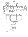
- FIG. 7A A further apparatus embodying the present invention is illustrated in Figures 7A and 7B.
- Figure 7A is a schematic view for assistance in explanation of the operation of the apparatus
- Figure 7B is a plan view illustrating the layout of various parts of the apparatus.
- Air in a main chamber 31 of an apparatus for electron beam exposure is exhausted in a known manner by a vacuum pump ⁇ not shown) through an exhaust valve 32 to maintain the main chamber 31 in vacuum.
- a stage 33 is provided in the main chamber 31, and a sample such as wafer 35 is placed on a sample holder 34 on the stage 33.
- Electron beams 38, to be used for electron beam exposure, from a cathode 37 of an electron gun 36 of conventional structure are irradiated onto the sample 35 to write a predetermined exposure pattern. In this case, negative photo resist emulsion is coated on the sample 35 for pattern exposure.
- the sample 35 after exposure, is taken out as loaded on the sample holder 34 into a sub--chamber 40 through a first gate valve 39.
- an exhaust valve 41 is opened for operation of a vacuum pump (not shown) to keep the sub-chamber 40 in vacuum in advance, and with the main chamber 31 being kept in operable vacuum, the first gate valve 39 is then closed.
- An inlet valve 42 is opened to introduce into the sub-chamber 40 non-oxidising gas which does not contain oxygen, or a gas that contains oxygen atoms, such as nitrogen, argon, helium or a mixture of these. (Of course, as indicated above, an amount of oxygen of at most 1% by volume may be included).
- a third gate valve 44b is opened.
- the sample 35 is removed from the sample holder 34 and taken into the gas chamber 44.
- the above described gas 43 enters the gas chamber 44 through an inlet valve 45 and is exhausted through an exhaust or a second gate valve 44a, so that there is always a continuous flow of non-oxidising gas 43.
- a first roller 47 for a belt conveyor 46 Internally of the gas chamber 44 there is provided a first roller 47 for a belt conveyor 46, and a second roller 48 is provided outside the gas chamber 44.
- the belt conveyor 46 surrounds these two rollers, and the samples 35 taken out of the sub-chamber 40 are successively placed on , and carried by, the belt conveyor 46. Samples 35 are gradually moved, staying within the gas chamber 44, for a predetermined period of time during which the curing effect described above takes place.
- the samples 35 taken out of the gas chamber 44 through an exhaust port 44a are exposed to the outside air for the first time and are placed in a cassette 49.
- a next sample 35 to be placed in main chamber 31 is introduced through a sample insert chamber 50 shown in Figure 7B.
- a third gate 51 is opened, and the sample 35 is carried into the sub-chamber 40.
- the insides of the sample insert chamber 50 and the sub-chamber 40 are generally kept in the same state as the outside atmosphere, and curing is effected with the second gate valve 44a closed. It.will be clearly understood that for delivery of the next sample the first gate 39 is closed, and when the next sample 35 is secured on the sample holder 34 in the sub-chamber 40, the exhaust valve 41 is opened to keep the sub-chamber 40 in vacuum, then the first gate 39 is opened and the sample holder 34 with the sample 35 thereon is placed on the XY stage 33. Thus, the sample is positioned at a predetermined position ready for exposure.
- the sample insert chamber 50 and the sub-chamber 40 are kept in the same condition as the outside atmosphere at the time when a next sample is brought in.
- the second gate 44a may be left open. It will be understood that, because of this, the second gate valve 44a can be constructed easily without being subjected to severe conditions.
- oxygen in a proportion less than or not greater than 1% in volume may harmlessly be mixed into the non-oxidising gas during the curing.
- the volume of oxygen can be held down to less than 1% by continuously supplying the non-oxidising gas.
- Figure 8 illustrates another apparatus embodying the present invention.
- 61 is a main chamber corresponding to main chamber 31 in Figure 7A
- 69 is a valve corresponding to valve 39
- items 64, 70, 74, 74e, 76, 79, 80 and 81 correspond to items 34, 40, 44, 44b, 46, 49, 50 and 51 in 7A.
- placing of a sample 63 on a sample holder 64 is not carried out in a sub-chamber 70. Instead, setting up of the sample 63 from a sample introduction chamber 80 and removal of sample 63 from a belt conveyor 76 into a cassette 79 are effected by means of the sample holder 64 provided in a gas chamber 74.
- Figure 9 illustrates a further embodiment of the present invention.
- items 110, 111, 91, 99, 100, 104b, 107, 106 and 109 correspond in general function to items 50, 51, 31, 39, 40 , 44b, 44, 46 and 49 in Figure 7A.
- a sample introduction chamber 110.- is placed near one side of a main chamber 91. Because of this arrangement, an entire process can be carried out using a belt conveyor 106 along a production line as follows : Introduction of samples (in a sub-chamber 110) - exposure (in a main chamber 91) - curing (in sub-chamber 100) - removal of samples (in chamber 107)- placing of the samples in a cassette 109.
- This arrangement avoids complexities of structure such as might arise were the sample introduction chamber l10 annexed to or combined with a sub-chamber 100 or gas chamber 107 .
- a method embodying the present invention makes it possible to form patterns with a high degree of precision, employing non-oxidising gas in place of a vacuum. Since samples to be exposed are moved in the non-oxidising gas handling thereof is facilitated. This serves to reduce the cost of manufacture of semiconductor devices such as highly integrated circuits.
- Apparatus embodying the present invention structured and operated as described above can provide continuous and effective exposure with little time wastage. As samples are set up and removed not in vacuum, handling of samples is simplified, with the samples showing no signs of the curing effect.
- the method and apparatus of the present invention are not limited to cases in which electron beams are used.
- the method and apparatus are just as effective when ion beams, soft X-ray beams or the like are employed.
- An exposure method embodying the present invention has a feature that, after a film of negative photoresist emulsion on a substrate has been exposed for pattern writing in vacuum to chargedparticle beams or soft X-ray beams, the substrate coated with the photoresist film is transferred to, and kept in, a chamber filled with non-oxidising gas, then the substrate is taken out into the outside atmosphere. Thereby, curing effect on the photoresist film is avoided, enabling formation of fine patterns with precision.
- such a method can be carried out, the apparatus having a structure such that a gas chamber filled with non-oxidising gas is connected to a chamber where exposure is carried out, and the substrate, after such exposure, is kept in an atmosphere of non-oxidising gas in the gas chamber before being taken out into the outside atmosphere.
Landscapes
- Physics & Mathematics (AREA)
- General Physics & Mathematics (AREA)
- Electron Beam Exposure (AREA)
- Exposure And Positioning Against Photoresist Photosensitive Materials (AREA)
- Photosensitive Polymer And Photoresist Processing (AREA)
- Drying Of Semiconductors (AREA)
Applications Claiming Priority (2)
| Application Number | Priority Date | Filing Date | Title |
|---|---|---|---|
| JP175634/80 | 1980-12-12 | ||
| JP55175634A JPS5799639A (en) | 1980-12-12 | 1980-12-12 | Treatment of negative type resist |
Publications (3)
| Publication Number | Publication Date |
|---|---|
| EP0054412A2 true EP0054412A2 (de) | 1982-06-23 |
| EP0054412A3 EP0054412A3 (en) | 1983-06-01 |
| EP0054412B1 EP0054412B1 (de) | 1986-04-23 |
Family
ID=15999509
Family Applications (1)
| Application Number | Title | Priority Date | Filing Date |
|---|---|---|---|
| EP81305824A Expired EP0054412B1 (de) | 1980-12-12 | 1981-12-10 | Verfahren und Vorrichtung zum Behandeln einer negativen Photoresistschicht |
Country Status (4)
| Country | Link |
|---|---|
| US (2) | US4426439A (de) |
| EP (1) | EP0054412B1 (de) |
| JP (1) | JPS5799639A (de) |
| DE (1) | DE3174490D1 (de) |
Cited By (5)
| Publication number | Priority date | Publication date | Assignee | Title |
|---|---|---|---|---|
| EP0103052A1 (de) * | 1982-08-25 | 1984-03-21 | Fujitsu Limited | Verfahren zur Erzeugung einer bemusterten Resistschicht auf einem Halbleiterkörper |
| WO1986003033A1 (en) * | 1984-11-09 | 1986-05-22 | American Telephone & Telegraph | Fabrication of microminiature devices |
| US5120634A (en) * | 1982-08-25 | 1992-06-09 | Fujitsu Limited | Method for forming patterned resist layer on semiconductor body |
| RU2126567C1 (ru) * | 1996-09-21 | 1999-02-20 | Самсунг Электроникс Ко, Лтд. | Состав разбавителя для смывания ненужного фоторезиста на пластине в процессе изготовления полупроводниковых устройств (варианты) и способ смывания ненужного фоторезиста (варианты) |
| US5962196A (en) * | 1991-04-08 | 1999-10-05 | Intel Corporation | Deep ultraviolet light photoresist processing |
Families Citing this family (15)
| Publication number | Priority date | Publication date | Assignee | Title |
|---|---|---|---|---|
| GB2142158A (en) * | 1983-05-25 | 1985-01-09 | Philips Electronic Associated | Electron lithography masks |
| JP2652072B2 (ja) * | 1990-02-26 | 1997-09-10 | キヤノン株式会社 | 遮光層の形成方法 |
| JP3148353B2 (ja) * | 1991-05-30 | 2001-03-19 | ケーエルエー・インストルメンツ・コーポレーション | 電子ビーム検査方法とそのシステム |
| US5439780A (en) * | 1992-04-29 | 1995-08-08 | At&T Corp. | Energy sensitive materials and methods for their use |
| JP3730263B2 (ja) * | 1992-05-27 | 2005-12-21 | ケーエルエー・インストルメンツ・コーポレーション | 荷電粒子ビームを用いた自動基板検査の装置及び方法 |
| JP3734095B2 (ja) * | 1994-09-12 | 2006-01-11 | 株式会社ニコン | 基板処理装置 |
| EP1124252A2 (de) * | 2000-02-10 | 2001-08-16 | Applied Materials, Inc. | Verfahren und Vorrichtung zur Verarbeitung von Substraten |
| EP1315957A4 (de) * | 2000-08-17 | 2006-10-11 | Yeda Res & Dev | Verfahren zur identifikation und quantifikation biologischer moleküle und vorrichtung dafür |
| WO2002045153A1 (fr) * | 2000-12-01 | 2002-06-06 | Ebara Corporation | Procede et appareil d'inspection utilisant un faisceau d'electrons, et procede de production de dispositif utilisant celui-ci |
| JP4966922B2 (ja) * | 2008-07-07 | 2012-07-04 | 東京エレクトロン株式会社 | レジスト処理装置、レジスト塗布現像装置、およびレジスト処理方法 |
| US8698104B2 (en) * | 2009-11-09 | 2014-04-15 | Varian Semiconductor Equipment Associates, Inc. | System and method for handling multiple workpieces for matrix configuration processing |
| DE102010008296A1 (de) * | 2010-02-17 | 2011-08-18 | Carl Zeiss NTS GmbH, 73447 | Laserbearbeitungssystem, Objekthalter und Laserbearbeitungsverfahren |
| JP5865125B2 (ja) * | 2012-03-02 | 2016-02-17 | 株式会社日立ハイテクノロジーズ | 荷電粒子線装置 |
| KR20160039957A (ko) * | 2014-10-02 | 2016-04-12 | 삼성전자주식회사 | 이온 발생기를 갖는 기판 이송 시스템 |
| US9583307B2 (en) * | 2015-07-01 | 2017-02-28 | Applied Materials Israel Ltd. | System and method for controlling specimen outgassing |
Family Cites Families (11)
| Publication number | Priority date | Publication date | Assignee | Title |
|---|---|---|---|---|
| FR1601513A (de) * | 1968-12-26 | 1970-08-24 | ||
| JPS5395189A (en) * | 1977-01-31 | 1978-08-19 | Hitachi Ltd | Fluorescent substance |
| JPS53124397A (en) * | 1977-04-06 | 1978-10-30 | Shigeru Kohiyama | Moving device |
| US4185202A (en) * | 1977-12-05 | 1980-01-22 | Bell Telephone Laboratories, Incorporated | X-ray lithography |
| JPS5511217A (en) | 1978-07-10 | 1980-01-26 | Nippon Telegr & Teleph Corp <Ntt> | Pattern forming method using radiation sensitive high polymer |
| JPS5569265A (en) * | 1978-11-15 | 1980-05-24 | Hitachi Ltd | Pattern-forming method |
| JPS5568622A (en) * | 1978-11-17 | 1980-05-23 | Hitachi Ltd | Sample replacing device at pattern drawing apparatus by electron beam |
| JPS5596942A (en) * | 1979-01-19 | 1980-07-23 | Matsushita Electric Ind Co Ltd | Method and apparatus for producing minute pattern |
| JPS55146932A (en) * | 1979-05-04 | 1980-11-15 | Hitachi Ltd | Specimen-exchanging device in electronic beam depicting device |
| US4239787A (en) * | 1979-06-25 | 1980-12-16 | Bell Telephone Laboratories, Incorporated | Semitransparent and durable photolithography masks |
| JPS5691425A (en) * | 1979-12-25 | 1981-07-24 | Seiko Epson Corp | Resist heat treatment device |
-
1980
- 1980-12-12 JP JP55175634A patent/JPS5799639A/ja active Granted
-
1981
- 1981-12-10 DE DE8181305824T patent/DE3174490D1/de not_active Expired
- 1981-12-10 EP EP81305824A patent/EP0054412B1/de not_active Expired
- 1981-12-11 US US06/329,941 patent/US4426439A/en not_active Expired - Lifetime
-
1983
- 1983-07-05 US US06/510,584 patent/US4508968A/en not_active Expired - Fee Related
Cited By (5)
| Publication number | Priority date | Publication date | Assignee | Title |
|---|---|---|---|---|
| EP0103052A1 (de) * | 1982-08-25 | 1984-03-21 | Fujitsu Limited | Verfahren zur Erzeugung einer bemusterten Resistschicht auf einem Halbleiterkörper |
| US5120634A (en) * | 1982-08-25 | 1992-06-09 | Fujitsu Limited | Method for forming patterned resist layer on semiconductor body |
| WO1986003033A1 (en) * | 1984-11-09 | 1986-05-22 | American Telephone & Telegraph | Fabrication of microminiature devices |
| US5962196A (en) * | 1991-04-08 | 1999-10-05 | Intel Corporation | Deep ultraviolet light photoresist processing |
| RU2126567C1 (ru) * | 1996-09-21 | 1999-02-20 | Самсунг Электроникс Ко, Лтд. | Состав разбавителя для смывания ненужного фоторезиста на пластине в процессе изготовления полупроводниковых устройств (варианты) и способ смывания ненужного фоторезиста (варианты) |
Also Published As
| Publication number | Publication date |
|---|---|
| JPS5799639A (en) | 1982-06-21 |
| EP0054412B1 (de) | 1986-04-23 |
| DE3174490D1 (en) | 1986-05-28 |
| US4508968A (en) | 1985-04-02 |
| US4426439A (en) | 1984-01-17 |
| EP0054412A3 (en) | 1983-06-01 |
| JPH023494B2 (de) | 1990-01-23 |
Similar Documents
| Publication | Publication Date | Title |
|---|---|---|
| EP0054412B1 (de) | Verfahren und Vorrichtung zum Behandeln einer negativen Photoresistschicht | |
| US5601686A (en) | Wafer transport method | |
| TWI286339B (en) | Method for improving surface roughness of processed film of substrate and apparatus for processing substrate | |
| JP2003151895A (ja) | 現像処理方法および現像液塗布装置 | |
| US20100307683A1 (en) | Substrate treatment method and substrate treatment apparatus | |
| US4307176A (en) | Method of forming a pattern | |
| US4806456A (en) | Dry development method for a resist film and an apparatus therefor | |
| EP0197286B1 (de) | Trockenentwicklungsverfahren für Schutzlackfilme | |
| US6864144B2 (en) | Method of stabilizing resist material through ion implantation | |
| US4900938A (en) | Method of treating photoresists | |
| US20060128160A1 (en) | Photoresist strip using solvent vapor | |
| US20050170266A1 (en) | Method to recover the exposure sensitivity of chemically amplified resins from post coat delay effect | |
| JPH0252449A (ja) | 基板のロード・アンロード方法 | |
| US20230064333A1 (en) | Method of cleaning substrate for blank mask, substrate for blank mask, and blank mask including the same | |
| JP2002208548A (ja) | レジストパターン形成方法 | |
| JP2624168B2 (ja) | パターン形成方法および電子線描画装置 | |
| JP2563689B2 (ja) | プラズマ反応装置 | |
| JPH02848B2 (de) | ||
| JPH03116819A (ja) | 半導体装置の製造方法および装置 | |
| US20240288775A1 (en) | Substrate processing method, substrate processing apparatus and substrate processing system | |
| JP3371002B2 (ja) | ウェハの搬送方法 | |
| JPS62241325A (ja) | 半導体基板などのマ−キング方法 | |
| JP2008091653A (ja) | 塗布・現像処理方法 | |
| JP2008140985A (ja) | パターン形成方法 | |
| JPS5938728B2 (ja) | 帯電粒子ビ−ム露光装置 |
Legal Events
| Date | Code | Title | Description |
|---|---|---|---|
| PUAI | Public reference made under article 153(3) epc to a published international application that has entered the european phase |
Free format text: ORIGINAL CODE: 0009012 |
|
| AK | Designated contracting states |
Designated state(s): DE FR GB NL |
|
| PUAL | Search report despatched |
Free format text: ORIGINAL CODE: 0009013 |
|
| AK | Designated contracting states |
Designated state(s): DE FR GB NL |
|
| 17P | Request for examination filed |
Effective date: 19830715 |
|
| GRAA | (expected) grant |
Free format text: ORIGINAL CODE: 0009210 |
|
| AK | Designated contracting states |
Kind code of ref document: B1 Designated state(s): DE FR GB NL |
|
| ET | Fr: translation filed | ||
| REF | Corresponds to: |
Ref document number: 3174490 Country of ref document: DE Date of ref document: 19860528 |
|
| PLBE | No opposition filed within time limit |
Free format text: ORIGINAL CODE: 0009261 |
|
| STAA | Information on the status of an ep patent application or granted ep patent |
Free format text: STATUS: NO OPPOSITION FILED WITHIN TIME LIMIT |
|
| 26N | No opposition filed | ||
| PGFP | Annual fee paid to national office [announced via postgrant information from national office to epo] |
Ref country code: GB Payment date: 19921013 Year of fee payment: 12 |
|
| PGFP | Annual fee paid to national office [announced via postgrant information from national office to epo] |
Ref country code: FR Payment date: 19921221 Year of fee payment: 12 |
|
| PGFP | Annual fee paid to national office [announced via postgrant information from national office to epo] |
Ref country code: NL Payment date: 19921231 Year of fee payment: 12 |
|
| PGFP | Annual fee paid to national office [announced via postgrant information from national office to epo] |
Ref country code: DE Payment date: 19930226 Year of fee payment: 12 |
|
| PG25 | Lapsed in a contracting state [announced via postgrant information from national office to epo] |
Ref country code: GB Effective date: 19931210 |
|
| PG25 | Lapsed in a contracting state [announced via postgrant information from national office to epo] |
Ref country code: NL Effective date: 19940701 |
|
| GBPC | Gb: european patent ceased through non-payment of renewal fee |
Effective date: 19931210 |
|
| NLV4 | Nl: lapsed or anulled due to non-payment of the annual fee | ||
| PG25 | Lapsed in a contracting state [announced via postgrant information from national office to epo] |
Ref country code: FR Effective date: 19940831 |
|
| PG25 | Lapsed in a contracting state [announced via postgrant information from national office to epo] |
Ref country code: DE Effective date: 19940901 |
|
| REG | Reference to a national code |
Ref country code: FR Ref legal event code: ST |