EP0048862A1 - Verfahren zur Messung von Widerständen und Kapazitäten von elektronischen Bauelementen - Google Patents
Verfahren zur Messung von Widerständen und Kapazitäten von elektronischen Bauelementen Download PDFInfo
- Publication number
- EP0048862A1 EP0048862A1 EP81107151A EP81107151A EP0048862A1 EP 0048862 A1 EP0048862 A1 EP 0048862A1 EP 81107151 A EP81107151 A EP 81107151A EP 81107151 A EP81107151 A EP 81107151A EP 0048862 A1 EP0048862 A1 EP 0048862A1
- Authority
- EP
- European Patent Office
- Prior art keywords
- component
- resistance
- capacitance
- measuring
- electronic components
- Prior art date
- Legal status (The legal status is an assumption and is not a legal conclusion. Google has not performed a legal analysis and makes no representation as to the accuracy of the status listed.)
- Granted
Links
Images
Classifications
-
- G—PHYSICS
- G01—MEASURING; TESTING
- G01R—MEASURING ELECTRIC VARIABLES; MEASURING MAGNETIC VARIABLES
- G01R27/00—Arrangements for measuring resistance, reactance, impedance, or electric characteristics derived therefrom
-
- G—PHYSICS
- G01—MEASURING; TESTING
- G01R—MEASURING ELECTRIC VARIABLES; MEASURING MAGNETIC VARIABLES
- G01R31/00—Arrangements for testing electric properties; Arrangements for locating electric faults; Arrangements for electrical testing characterised by what is being tested not provided for elsewhere
- G01R31/28—Testing of electronic circuits, e.g. by signal tracer
- G01R31/302—Contactless testing
- G01R31/305—Contactless testing using electron beams
Definitions
- the invention relates to a method for measuring resistances and capacitances of electronic components.
- the invention has for its object to measure the resistances and capacities of electronic components without stress.
- This measuring method can be used to determine significantly smaller capacities than is possible according to the prior art.
- the method customary in electron beam measurement technology is advantageously carried out with the aid of a secondary electron Spectrometer applied, with which the potential change on the component is first measured, from which the potential curve U (t) is then determined.
- the frequency of the electron pulses synchronized with the frequency of the signal on a component that is part of the circuit, so that the resistance R and the capacitance C on this component are determined dynamically, from which then switched on to this component Load can be closed.
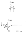
- FIG. 1 shows an equivalent circuit diagram
- FIG. 2 shows the determination of resistance R and capacitance C from the potential curve U (t).
- the equivalent circuit diagram applicable to this measuring method of resistances and capacitances of electronic components is shown in FIG. 1.
- the charge of the component for t ⁇ ⁇ ( ⁇ 5 ⁇ RC) reaches a saturation voltage U S , from which the resistance R can be calculated if the current I A is known.
- Arrangements can be used for the measuring method according to the invention, such as those e.g. by H.-P. Feuerbaum are described in "VLSI testing using the electron probe", SEM / 1979 / Vol. 1, 285-296, (1979).
- the electron current is pulsed into the electronic component.
- the potential change within the pulse is queried.
- the method commonly used in electron beam measuring technology with the aid of a secondary electron spectrometer is advantageously used.
- the resistance R and the capacitance C can also be determined dynamically. The measurement of the resistance R and the capacitance C can then be used to draw conclusions about the load connected to the component in question.
Abstract
Description
- Die Erfindung betrifft ein Verfahren zur Messung von Widerständen und Kapazitäten von elektronischen Bauelementen..
- Bisher wurde die Messung von Widerständen und Kapazitäten von elektronischen Bauelementen mit einer mechanischen Spitze durchgeführt. Die kleinste nach diesem Verfahren meßbare Kapazität beträgt 1 pF.
- Der Erfindung liegt die Aufgabe zugrunde, Widerstände und Kapazitäten von elektronischen Bauelementen belastungsfrei zu messen.
- Diese Aufgabe wird erfindungsgemäß dadurch gelöst, daß einem Bauelement mit dem Widerstand R und der Kapazität C durch einen gepulsten Elektronenstrahl ein-Strom IA aufgeprägt wird, gemäß IA = IR + IC9 wobei der Potentialverlauf U(t), der sich während des Pulses am elektronischen Bauelement infolge des aufgeprägten Stromes IA ergibt, gemessen wird, woraus sich.durch entsprechende Auswahl von zwei Meßpunkten U(t1), U(t2) bei bekanntem Strom IA der Widerstand R und die Kapazität C bestimmen lassen. Mit diesem Meßverfahren lassen sich wesentlich kleinere Kapazitäten als nach dem Stand der Technik möglich bestimmen.
- Zum Messen des Potentialverlaufs U(t) wird vorteilhafterweise das in der Elektronenstrahl-Meßtechnik übliche Verfahren mit Hilfe eines Sekundärelektronen-Spektrometers angewandt, mit dem zunächst die Potentialänderung am Bauelement gemessen-wird, woraus sodann der Potentialverlauf U(t) bestimmt wird.
- Als die zur Bestimmung des Widerstands R und der Kapazität C erforderlichen beiden Meßpunkte U(t1), U(t2) werden zweckmäßigerweise die Sättigungsspannung Us = U (t→∞) ≈ U(5RC) = U(t1)und US-0,63 = U(t = RC) = U(t2) herangezogen.
- In einer vorteilhaften Ausgestaltung der Erfindung wird bei der Messung an einer Schaltung, z.B. einer integrierten Schaltung, die Frequenz der Elektronenpulse mit der Frequenz des Signals an einem Bauelement, das ein Teil der Schaltung ist, synchronisiert, so daß der Widerstand R und die Kapazität C an diesem Bauelement dynamisch bestimmt werden, woraus dann auf die an dieses Bauelement zugeschaltete Last geschlossen werden kann.
- Die Erfindung wird in der Zeichnung näher dargestellt.
- Figur 1 zeigt ein Ersatzschaltbild.
- Figur 2 zeigt die Bestimmung von Widerstand R und Kapazität C aus dem Potentialverlauf U(t).
- Einem Bauelement mit dem Widerstand R und der Kapazität C wird bei einem erfindungsgemäßen Meßverfahren durch den Elektronenstrahl ein Strom IA aufgeprägt gemäß 1A = IR + IC. Das für dieses Meßverfahren von Widerständen und Kapazitäten von elektronischen Bauelementen zutreffende Ersatzschaltbild zeigt Figur 1.
- Für die resultierenden Aufladungen des Bauelements gilt folgende Differentialgleichung .


- Demnach erreicht die Aufladung des Bauelements für t→∞ (≈5 · RC) eine Sättigungsspannung US, aus der sich bei bekanntem Strom IA der Widerstand R berechnen läßt. Die Kapazität C berechnet sich aus der Beziehung U(t = RC) = US · 0,63, wobei für den Widerstand R der aus der Sättigungsspannung US gewonnene Widerstandswert R einzusetzen ist. Wenn der Potentialverlauf U (t) experimentell gemessen wurde, so können z.B. der Widerstand R und die Kapazität C vorteilhafterweise grafisch aus dem Potentialverlauf U(t) gewonnen werden, wie in Figur 2 gezeigt wird.
- Bei einer Potentialauflösung von 1 mV, einer Zeitauflösung von 5 ns und einem Elektronenstrom IA von 10-7 A errechnet sich als Einsatzbereich des Verfahrens


- Für das erfindungsgemäße Meßverfahren können Anordnungen herangezogen werden, wie sie z.B. von H.-P. Feuerbaum beschrieben werden in "VLSI testing using the electron probe", SEM/1979/Vol. 1, 285-296, (1979). Für die Messung der Aufladung wird der Elektronenstrom dem elektronischen Bauelement pulsförmig eingeprägt. Die Potentialänderung innerhalb des Pulses wird abgefragt. Dazu wird vorteilhafterweise das in der Elektronenstrahl-Meßtechnik übliche Verfahren mit Hilfe eines Sekundärelektronen-Spektrometers verwendet.
- Wird z.B. bei der erfindungsgemäßen Messung an einer integrierten Schaltung die Frequenz der Elektronenpulse mit der Frequenz des Signals am Meßpunkt synchronisiert, so können der Widerstand R und die Kapazität C auch dynamisch bestimmt werden. Aus der Messung des Widerstandes R und der Kapazität C kann dann auf die an das betreffende Bauelement zugeschaltete Last geschlossen werden.
Claims (4)
Applications Claiming Priority (2)
| Application Number | Priority Date | Filing Date | Title |
|---|---|---|---|
| DE3036734 | 1980-09-29 | ||
| DE19803036734 DE3036734A1 (de) | 1980-09-29 | 1980-09-29 | Verfahren zur messung von widerstaenden und kapazitaeten von elektronischen bauelementen |
Publications (2)
| Publication Number | Publication Date |
|---|---|
| EP0048862A1 true EP0048862A1 (de) | 1982-04-07 |
| EP0048862B1 EP0048862B1 (de) | 1985-03-20 |
Family
ID=6113156
Family Applications (1)
| Application Number | Title | Priority Date | Filing Date |
|---|---|---|---|
| EP81107151A Expired EP0048862B1 (de) | 1980-09-29 | 1981-09-10 | Verfahren zur Messung von Widerständen und Kapazitäten von elektronischen Bauelementen |
Country Status (4)
| Country | Link |
|---|---|
| US (1) | US4460866A (de) |
| EP (1) | EP0048862B1 (de) |
| JP (1) | JPS5786768A (de) |
| DE (2) | DE3036734A1 (de) |
Cited By (4)
| Publication number | Priority date | Publication date | Assignee | Title |
|---|---|---|---|---|
| DE3235461A1 (de) * | 1982-09-24 | 1984-03-29 | Siemens AG, 1000 Berlin und 8000 München | Verfahren zur kontaktlosen pruefung eines objekts, insbesondere von mikroverdrahtungen, mit einer korpuskularstrahl-sonde |
| WO1987007731A1 (en) * | 1986-06-06 | 1987-12-17 | Santa Barbara Research Center | Electron-beam probing of photodiodes |
| EP0328869A2 (de) * | 1988-02-19 | 1989-08-23 | Microelectronics and Computer Technology Corporation | Elektroumstrahlprüfung von elektronischen Komponenten |
| FR2726369A1 (fr) * | 1994-11-02 | 1996-05-03 | Alcatel Cable | Procede de mesure du declin de potentiel et de la mobilite electronique d'un materiau |
Families Citing this family (16)
| Publication number | Priority date | Publication date | Assignee | Title |
|---|---|---|---|---|
| EP0166912B1 (de) * | 1984-06-01 | 1990-08-29 | Siemens Aktiengesellschaft | Verfahren zur elektrischen Prüfung von Mikroverdrahtungen mit Hilfe von Korpuskularsonden |
| DE3576213D1 (de) * | 1984-09-18 | 1990-04-05 | Integrated Circuit Testing | Gegenfeld-spektrometer fuer die elektronenstrahl-messtechnik. |
| DE3677034D1 (de) * | 1985-03-11 | 1991-02-28 | Nippon Telegraph & Telephone | Methode und geraet zum testen eines integrierten elektronischen bauteils. |
| JPH0682718B2 (ja) * | 1985-08-12 | 1994-10-19 | 日本電信電話株式会社 | 電子デバイスの試験装置およびその使用方法 |
| US5245294A (en) * | 1991-03-08 | 1993-09-14 | General Electric Company | Method for evaluating operability of filter components in power conversion system |
| DE19525081B4 (de) * | 1995-07-10 | 2006-06-29 | Display Products Group, Inc., Hayward | Verfahren und Vorrichtung zum Testen der Funktion von Mikrostrukturelementen |
| US6359451B1 (en) | 2000-02-11 | 2002-03-19 | Image Graphics Incorporated | System for contactless testing of printed circuit boards |
| AU3354401A (en) | 2000-02-14 | 2001-08-20 | Eco 3 Max Inc. | Process for removing volatile organic compounds from an air stream and apparatustherefor |
| JP4015352B2 (ja) * | 2000-02-22 | 2007-11-28 | 株式会社日立製作所 | 荷電粒子ビームを用いた検査方法 |
| US7012438B1 (en) * | 2002-07-10 | 2006-03-14 | Kla-Tencor Technologies Corp. | Methods and systems for determining a property of an insulating film |
| US7248062B1 (en) | 2002-11-04 | 2007-07-24 | Kla-Tencor Technologies Corp. | Contactless charge measurement of product wafers and control of corona generation and deposition |
| US7893703B2 (en) * | 2005-08-19 | 2011-02-22 | Kla-Tencor Technologies Corp. | Systems and methods for controlling deposition of a charge on a wafer for measurement of one or more electrical properties of the wafer |
| JP5103050B2 (ja) * | 2007-04-06 | 2012-12-19 | 株式会社日立ハイテクノロジーズ | 電子線応用装置 |
| FR3112393B1 (fr) * | 2020-07-10 | 2022-07-08 | Centre Nat Rech Scient | Dispositif de détermination de la résistance électrique d’un système et procédé associé |
| EP3968035A1 (de) * | 2020-09-11 | 2022-03-16 | ASML Netherlands B.V. | System und verfahren zur verzögerungszeitmessung |
| WO2023217355A1 (en) * | 2022-05-10 | 2023-11-16 | Applied Materials, Inc. | Methods and apparatuses for identifying defective electrical connections of a substrate |
Citations (2)
| Publication number | Priority date | Publication date | Assignee | Title |
|---|---|---|---|---|
| DE2137619A1 (de) * | 1971-07-28 | 1973-02-08 | Ibm Deutschland | Verfahren zum pruefen des elektrischen durchganges |
| DE2215179B2 (de) * | 1972-03-28 | 1976-07-22 | Siemens AG, 1000 Berlin und 8000 München | Verfahren zur beruehrungslosen messung von elektrischen widerstaenden |
Family Cites Families (7)
| Publication number | Priority date | Publication date | Assignee | Title |
|---|---|---|---|---|
| US3239664A (en) * | 1963-04-23 | 1966-03-08 | High Voltage Engineering Corp | Charged particle beam current measuring device |
| CH408202A (de) * | 1963-08-09 | 1966-02-28 | Siemens Ag | Verfahren zur Bestimmung des elektrischen Widerstandes eines Körpers aus extrem reinem Halbleitermaterial für elektronische Zwecke |
| US3403332A (en) * | 1964-09-25 | 1968-09-24 | Hitachi Ltd | Apparatus for measuring impedance of a specimen employing two opposite polarity charged particle beam probes |
| US3373353A (en) * | 1965-09-30 | 1968-03-12 | Navy Usa | Electron beam scanning system for quality control of materials |
| US3464007A (en) * | 1966-11-22 | 1969-08-26 | Northern Electric Co | Apparatus for sorting electrical components by current consumption at prescribed voltage |
| US3531716A (en) * | 1967-06-16 | 1970-09-29 | Agency Ind Science Techn | Method of testing an electronic device by use of an electron beam |
| JPS51148495A (en) * | 1975-06-13 | 1976-12-20 | Ishikawajima Harima Heavy Ind Co Ltd | Resistance measuring device |
-
1980
- 1980-09-29 DE DE19803036734 patent/DE3036734A1/de not_active Withdrawn
-
1981
- 1981-07-20 US US06/284,827 patent/US4460866A/en not_active Expired - Fee Related
- 1981-09-10 EP EP81107151A patent/EP0048862B1/de not_active Expired
- 1981-09-10 DE DE8181107151T patent/DE3169396D1/de not_active Expired
- 1981-09-25 JP JP56151916A patent/JPS5786768A/ja active Pending
Patent Citations (2)
| Publication number | Priority date | Publication date | Assignee | Title |
|---|---|---|---|---|
| DE2137619A1 (de) * | 1971-07-28 | 1973-02-08 | Ibm Deutschland | Verfahren zum pruefen des elektrischen durchganges |
| DE2215179B2 (de) * | 1972-03-28 | 1976-07-22 | Siemens AG, 1000 Berlin und 8000 München | Verfahren zur beruehrungslosen messung von elektrischen widerstaenden |
Non-Patent Citations (1)
| Title |
|---|
| SCANNING ELECTRON MICROSCOPY, 1979 H.P. FEUERBAUM "VLSI Testing Using the Electron Probe" Seiten 285 bis 296 * |
Cited By (6)
| Publication number | Priority date | Publication date | Assignee | Title |
|---|---|---|---|---|
| DE3235461A1 (de) * | 1982-09-24 | 1984-03-29 | Siemens AG, 1000 Berlin und 8000 München | Verfahren zur kontaktlosen pruefung eines objekts, insbesondere von mikroverdrahtungen, mit einer korpuskularstrahl-sonde |
| WO1987007731A1 (en) * | 1986-06-06 | 1987-12-17 | Santa Barbara Research Center | Electron-beam probing of photodiodes |
| EP0328869A2 (de) * | 1988-02-19 | 1989-08-23 | Microelectronics and Computer Technology Corporation | Elektroumstrahlprüfung von elektronischen Komponenten |
| EP0328869A3 (de) * | 1988-02-19 | 1991-06-12 | Microelectronics and Computer Technology Corporation | Elektroumstrahlprüfung von elektronischen Komponenten |
| FR2726369A1 (fr) * | 1994-11-02 | 1996-05-03 | Alcatel Cable | Procede de mesure du declin de potentiel et de la mobilite electronique d'un materiau |
| EP0710848A1 (de) * | 1994-11-02 | 1996-05-08 | Alcatel Cable | Verfahren zur Messung des Spannungsabfalls und der Elektronenbeweglichkeit eines Materials |
Also Published As
| Publication number | Publication date |
|---|---|
| US4460866A (en) | 1984-07-17 |
| JPS5786768A (en) | 1982-05-29 |
| EP0048862B1 (de) | 1985-03-20 |
| DE3036734A1 (de) | 1982-05-06 |
| DE3169396D1 (en) | 1985-04-25 |
Similar Documents
| Publication | Publication Date | Title |
|---|---|---|
| EP0048862A1 (de) | Verfahren zur Messung von Widerständen und Kapazitäten von elektronischen Bauelementen | |
| DE3213866A1 (de) | Verfahren und schaltungsanordnung zur bestimmung des wertes des ohmschen widerstandes eines messobjekts | |
| DE2626976A1 (de) | Annaeherungssensor | |
| DE3138992A1 (de) | Abtastverfahren zur schnellen potentialbestimmung inder elektronenstrahl-messtechnik | |
| DE69630520T2 (de) | Bestimmung der dielektrischen eigenschaften von holz | |
| DE2701857A1 (de) | Messbruecke fuer vorrichtung zur werkstoffpruefung | |
| DE19638204C1 (de) | Vorrichtung zur Luftgütemessung | |
| DE2809154A1 (de) | Verfahren zur messung von daempfungsverlaeufen an vierpolen | |
| DE4133619C2 (de) | Verfahren und Vorrichtung zur Messung des Einschwingverhaltens | |
| EP0136591A1 (de) | Verfahren zum Messen niederfrequenter Signalverläufe innerhalb integrierter Schaltungen mit der Elektronensonde | |
| EP0438637A1 (de) | Verfahren und Anordnung zur Ermittlung eines Effektivwertes Ieff eines mit Hilfe eines Hallelementes und einer Verstärkeranordnung zu messenden Stromes | |
| DE2721353C3 (de) | Verfahren zur Erfassung von inneren Teilentladungsimpulsen elektrischer Isolierungen und Einrichtung zur Durchführung des Verfahrens | |
| DE2021811C3 (de) | Einrichtung zur Messung der Dielektrizitätskonstanten von Stoffen | |
| DE2620895B2 (de) | Einrichtung zur Messung der mittleren Rauhtiefe einer Werkstückoberfläche | |
| DE19613813A1 (de) | Vorrichtung zur Messung des Füllstands von Flüssigkeiten geringer Leitfähigkeit, insbesondere Wasser | |
| DE2643460C3 (de) | Schaltungsanordnung zum Messen von Strömen oder Spannungen | |
| CH647603A5 (en) | Device for measuring an ionising radiation with a connectable measuring probe | |
| AT256986B (de) | Verfahren und Einrichtung zur Prüfung von Isolierungen mit Gleichspannung | |
| DE2357195C3 (de) | Verfahren zur Prüfung des Teilungsverhältnisses eines Hochspannungsteilers und Anordnung zur Durchführung des Verfahrens | |
| DE2430907C3 (de) | Schaltungsanordnung zum Feststellen von Änderungen der Impedanz biologischer Objekte | |
| DE102018124090A1 (de) | Elektronische Schaltung für einen elektrochemischen Sensor und Verfahren zur Messung einer Impedanz von mindestens einem Messkanal des elektrochemischen Sensors | |
| DE2328087C3 (de) | Anordnung zur Messung von Kennwerten eines Oszillators | |
| DE910091C (de) | Einrichtung zur Messung der elektrischen Leitfaehigkeit von Fluessigkeiten | |
| AT393742B (de) | Digitaler wechselspannungs-effektivwertmesser | |
| DD212817A1 (de) | Anordnung zur messung des wellenwiderstandes von hochfrequenzkabeln |
Legal Events
| Date | Code | Title | Description |
|---|---|---|---|
| PUAI | Public reference made under article 153(3) epc to a published international application that has entered the european phase |
Free format text: ORIGINAL CODE: 0009012 |
|
| 17P | Request for examination filed |
Effective date: 19811028 |
|
| AK | Designated contracting states |
Designated state(s): DE FR GB NL |
|
| GRAA | (expected) grant |
Free format text: ORIGINAL CODE: 0009210 |
|
| AK | Designated contracting states |
Designated state(s): DE FR GB NL |
|
| REF | Corresponds to: |
Ref document number: 3169396 Country of ref document: DE Date of ref document: 19850425 |
|
| ET | Fr: translation filed | ||
| PLBE | No opposition filed within time limit |
Free format text: ORIGINAL CODE: 0009261 |
|
| STAA | Information on the status of an ep patent application or granted ep patent |
Free format text: STATUS: NO OPPOSITION FILED WITHIN TIME LIMIT |
|
| 26N | No opposition filed | ||
| PGFP | Annual fee paid to national office [announced via postgrant information from national office to epo] |
Ref country code: NL Payment date: 19870930 Year of fee payment: 7 |
|
| PG25 | Lapsed in a contracting state [announced via postgrant information from national office to epo] |
Ref country code: GB Effective date: 19890910 |
|
| PG25 | Lapsed in a contracting state [announced via postgrant information from national office to epo] |
Ref country code: NL Effective date: 19900401 |
|
| GBPC | Gb: european patent ceased through non-payment of renewal fee | ||
| NLV4 | Nl: lapsed or anulled due to non-payment of the annual fee | ||
| PG25 | Lapsed in a contracting state [announced via postgrant information from national office to epo] |
Ref country code: FR Effective date: 19900531 |
|
| PG25 | Lapsed in a contracting state [announced via postgrant information from national office to epo] |
Ref country code: DE Effective date: 19900601 |
|
| REG | Reference to a national code |
Ref country code: FR Ref legal event code: ST |