EP0046835A2 - Appareil de radiotélécommunication à canaux multiples pour les modes de fonctionnement "intercommunication" et/ou "téléphonie bidirectionnelle alternative" - Google Patents
Appareil de radiotélécommunication à canaux multiples pour les modes de fonctionnement "intercommunication" et/ou "téléphonie bidirectionnelle alternative" Download PDFInfo
- Publication number
- EP0046835A2 EP0046835A2 EP81101731A EP81101731A EP0046835A2 EP 0046835 A2 EP0046835 A2 EP 0046835A2 EP 81101731 A EP81101731 A EP 81101731A EP 81101731 A EP81101731 A EP 81101731A EP 0046835 A2 EP0046835 A2 EP 0046835A2
- Authority
- EP
- European Patent Office
- Prior art keywords
- circuit
- digital
- channel
- digital value
- voltage
- Prior art date
- Legal status (The legal status is an assumption and is not a legal conclusion. Google has not performed a legal analysis and makes no representation as to the accuracy of the status listed.)
- Granted
Links
Images

Classifications
-
- H—ELECTRICITY
- H03—ELECTRONIC CIRCUITRY
- H03J—TUNING RESONANT CIRCUITS; SELECTING RESONANT CIRCUITS
- H03J5/00—Discontinuous tuning; Selecting predetermined frequencies; Selecting frequency bands with or without continuous tuning in one or more of the bands, e.g. push-button tuning, turret tuner
- H03J5/02—Discontinuous tuning; Selecting predetermined frequencies; Selecting frequency bands with or without continuous tuning in one or more of the bands, e.g. push-button tuning, turret tuner with variable tuning element having a number of predetermined settings and adjustable to a desired one of these settings
- H03J5/0245—Discontinuous tuning using an electrical variable impedance element, e.g. a voltage variable reactive diode, in which no corresponding analogue value either exists or is preset, i.e. the tuning information is only available in a digital form
- H03J5/0272—Discontinuous tuning using an electrical variable impedance element, e.g. a voltage variable reactive diode, in which no corresponding analogue value either exists or is preset, i.e. the tuning information is only available in a digital form the digital values being used to preset a counter or a frequency divider in a phase locked loop, e.g. frequency synthesizer
- H03J5/0281—Discontinuous tuning using an electrical variable impedance element, e.g. a voltage variable reactive diode, in which no corresponding analogue value either exists or is preset, i.e. the tuning information is only available in a digital form the digital values being used to preset a counter or a frequency divider in a phase locked loop, e.g. frequency synthesizer the digital values being held in an auxiliary non erasable memory
-
- H—ELECTRICITY
- H04—ELECTRIC COMMUNICATION TECHNIQUE
- H04B—TRANSMISSION
- H04B1/00—Details of transmission systems, not covered by a single one of groups H04B3/00 - H04B13/00; Details of transmission systems not characterised by the medium used for transmission
- H04B1/38—Transceivers, i.e. devices in which transmitter and receiver form a structural unit and in which at least one part is used for functions of transmitting and receiving
- H04B1/40—Circuits
- H04B1/54—Circuits using the same frequency for two directions of communication
- H04B1/56—Circuits using the same frequency for two directions of communication with provision for simultaneous communication in two directions
Definitions
- the invention is based on a multi-channel radio device according to the preamble of the main claim.
- Multichannel two-way radios are known which are suitable for the “intercom” and / or “conditional intercom” modes.
- the desired radio channel is set with a channel button, which is used to control a PROM (programmable-read-only-memory) memory circuit.
- the PROM memory circuit emits coded signals at its output which are used to drive a PLL (phase-locked-loop) oscillator circuit.
- the PROM memory circuit is programmed in such a way that it only emits code signals for approved radio channels.
- the channel spacing is either 20 or 25 kHz.
- Such a multichannel two-way radio has the disadvantage that it has fixedly tuned input circuits with a switching bandwidth of up to 5 MHz which can be switched to the upper band or lower band in the operating mode "conditional two-way communication". Universal applicability of the multi-channel radio device in the entire available radio frequency range is therefore not possible.
- the multi-channel walkie-talkie according to the invention with the characterizing features of the main claim has the advantage that the high-frequency input circuits of the walkie-talkie are optimally coordinated for each selected radio channel.
- a multi-channel walkie-talkie is particularly advantageous, in which the logic combination circuit contains switching means with which, by forming the difference between a reference voltage, the size of which depends on the operating mode, the frequency band (upper band or lower band) and the channel grid, and an analogue derived from the first digital value Voltage the control voltage is generated.
- a control voltage can be provided which precisely matches the selection circuit or the selection circuits of the receiving part of the radio device to the reception frequency.
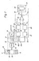
- a multi-channel radio device has a channel switch device 10 with a channel button 11, a mode switch 12 with the switch positions intercom (W), upper band (OB) and lower band (UB), a coding device 13 and a digital display device 14.
- the coding device 13 is connected to a PROM (programmable-read-only-memory) memory circuit 15.
- a first, second and third line connection 16, 17 and 21 lead from the PROM memory circuit to a PLL (phase-locked-loop) oscillator circuit 18, the output of which is connected to a mixer stage of the receiving part of the radio.
- a first, second and third branch 160, 170 and 210 of the first to third line connections 16, 17 and 21 lead to a logic logic circuit 22 which comprises the following construction stages.
- An evaluator 23 connected to branches 160, 170 and 210 is connected to a reference voltage switch 24, the output 25 of which is connected to a non-inverting input of an operational amplifier 26 connected as a differential amplifier.
- a digital / analog converter 28, whose output 29 is connected to an inverting input of the operational amplifier 26, is also connected to the branch 160 or the first line connection 16 via an adaptation stage 27.
- the adaptation stage-27 is a stage, for example formed by a buffer circuit, for adapting the output signal level of the PROM memory circuit 15 to the input of the digital / analog converter 28 and / or a stage for adapting the digital value on the first line connection 16 to that for the Digital / analog converter 28 required input digital value.
- An output 30 of the operational amplifier 26 is connected to an electronically tunable one Selection circuit 31 on, that is for example a high-frequency input circuit 32, the capacitance of which is partly formed by a capacitance variation diode 33.
- FIG. 2 In the more detailed block diagram in FIG. 2, construction stages corresponding to FIG. 1 are designated with the same reference numbers.
- the operation of the circuit described in FIGS. 1 and 2 is as follows.
- the coding device 13 inputs digital information, for example in the BCD code, which firstly contains the reception frequency of the radio channel set, secondly the selected operating mode (two-way communication or conditional two-way communication) and thirdly the selected band (upper band or lower band). This information is fed to the PROM memory circuit 15.
- the PROM memory circuit is first programmed in such a way that it outputs a digital value via the first line connection 16 to the PLL circuit 18 in accordance with the selected radio channel - if this is a permissible radio channel at all.
- the digital value corresponds to a certain division ratio, by which the PLL oscillator circuit is influenced in such a way that it outputs a certain oscillator frequency at its output, which is mixed in a mixing stage of the receiving part of the radio with the respective receiving frequency and forms a (first) intermediate frequency.
- the PROM memory circuit is programmed to over the second Line connection 17 outputs a digital value to the PLL oscillator circuit, which causes the oscillator frequencies generated to lie in the desired frequency grid.
- the PROM memory circuit also delivers a signal identifying the selected operating mode via the line connection 21.
- the last-mentioned signal can optionally also be derived directly from the operating mode switch 12; see. in Fig. 1 dashed line connections.
- the distance between the individual radio channels, i.e. the frequency grid, is 20 kHz or 25 kHz, for example.
- the evaluator 23 makes the following distinctions based on the signals brought to the logic logic circuit 22 via the first to third line connections 16, 17, 21 and the branches 160, 170, 210. It determines whether the operating mode "two-way communication" or “conditional two-way communication", whether a frequency of the upper band or the lower band and which channel grid has been selected with the channel switch device. A number of logic gates 35 are required for these distinctions.
- the evaluator 23 emits an output signal at its outputs, with which the reference voltage switch 24 is controlled. In the exemplary embodiment according to FIG.
- the evaluator 23 has six outputs 36 to 41, of which the outputs 36 and 37 are the upper band or lower band of the 20 k H z raster, the outputs 38 and 39 are the lower band or upper band of the 25th -kHz grid and the outputs 40 and 41 correspond to the intercom frequencies in the 25 kHz grid and in the 20 kHz grid, respectively.
- each of the outputs 36 to 41 is an electro controllable by the output signal African switch 42 to 47 assigned, with which an adjusting resistor 48 can be switched on.
- the adjusting resistors 48 are connected to a fixed DC voltage potential U and with their other connection via one of each of the switches 42 to 47 to the non-inverting input of the operational amplifier 26.
- Different settings of the adjusting resistors 48 lie at the non-inverting input of the operational amplifier 26, each after which of the switches 42 to 47 is closed, one of several reference voltages U ref1 ... 6 .
- the digital value which is guided from the line connection 16 or the branch 160 to the adaptation stage 27 and is dependent on the desired frequency is converted, for example, in the adaptation circuit into a correspondingly different digital value with which the digital / analog converter 28 can be controlled.
- U a and Ur ef By subtracting the voltages U a and Ur ef by means of the operational amplifier 26, one of the control voltages U St1 ... n is obtained at the output 30 of the operational amplifier.
- the respective control voltage is supplied to the capacitance variation diode 33 in such a way that its capacitance value changes in such a way that the selection circuit is tuned to the desired resonance frequency (reception frequency).
- the PROM memory circuit 15 If the operating mode switch 12 is in the switch position "two-way communication" (W), the PROM memory circuit 15 outputs a signal identifying the operating mode to the third connecting line 21, which signal is recognized by the evaluator 23. In connection with that by the Evaluator also determined channel grid of 20 kHz or 25 kHz, for example, one of the switches 46, 47 is then closed and a reference voltage U ref5 or U ref6 corresponding to the two-way communication and the relevant grid is generated. In parallel, the digital / analog converter 28 delivers an output voltage U a , which depends on the selected channel or the desired frequency. By forming the difference in the operational amplifier 26, a control voltage U St is then obtained which tunes the selection circuit 31 in the manner already mentioned above.
Priority Applications (1)
| Application Number | Priority Date | Filing Date | Title |
|---|---|---|---|
| AT81101731T ATE7831T1 (de) | 1980-08-28 | 1981-03-10 | Vielkanal-sprechfunkgeraet fuer die betriebsarten 'wechselsprechen' und/oder 'bedingtes gegensprechen'. |
Applications Claiming Priority (2)
| Application Number | Priority Date | Filing Date | Title |
|---|---|---|---|
| DE3032378 | 1980-08-28 | ||
| DE19803032378 DE3032378A1 (de) | 1980-08-28 | 1980-08-28 | Vielkanal-sprechfunkgeraet fuer die betriebsarten wechselsprechen und/oder bedingtes gegensprechen |
Publications (3)
| Publication Number | Publication Date |
|---|---|
| EP0046835A2 true EP0046835A2 (fr) | 1982-03-10 |
| EP0046835A3 EP0046835A3 (en) | 1982-09-01 |
| EP0046835B1 EP0046835B1 (fr) | 1984-06-06 |
Family
ID=6110558
Family Applications (1)
| Application Number | Title | Priority Date | Filing Date |
|---|---|---|---|
| EP81101731A Expired EP0046835B1 (fr) | 1980-08-28 | 1981-03-10 | Appareil de radiotélécommunication à canaux multiples pour les modes de fonctionnement "intercommunication" et/ou "téléphonie bidirectionnelle alternative" |
Country Status (3)
| Country | Link |
|---|---|
| EP (1) | EP0046835B1 (fr) |
| AT (1) | ATE7831T1 (fr) |
| DE (2) | DE3032378A1 (fr) |
Cited By (5)
| Publication number | Priority date | Publication date | Assignee | Title |
|---|---|---|---|---|
| EP0119439A2 (fr) * | 1983-03-16 | 1984-09-26 | ANT Nachrichtentechnik GmbH | Mélangeur à diode avec commande de tension de polarisation et son application |
| WO1987002202A1 (fr) * | 1985-10-01 | 1987-04-09 | Plessey Overseas Limited | Circuit de reglage de frequences et synthetiseur relatif |
| GB2194696A (en) * | 1986-03-26 | 1988-03-09 | Gen Electric | Digital radio communications devices |
| US4905305A (en) * | 1986-03-26 | 1990-02-27 | General Electric Company | Method and apparatus for controlling the frequency of operation and at least one further variable operating parameter of a radio communications device |
| EP0394358A1 (fr) * | 1988-01-07 | 1990-10-31 | Motorola, Inc. | Synthetiseur de frequences de basse tension et faible puissance |
Families Citing this family (1)
| Publication number | Priority date | Publication date | Assignee | Title |
|---|---|---|---|---|
| DE3626792A1 (de) * | 1986-08-08 | 1988-02-11 | Siemens Ag | Einrichtung zur stabilisierung der sende- und empfangsfrequenz eines uebertragungsgeraetes |
Citations (2)
| Publication number | Priority date | Publication date | Assignee | Title |
|---|---|---|---|---|
| US3715687A (en) * | 1972-04-05 | 1973-02-06 | Gte Sylvania Inc | Non-linear voltage generating apparatus |
| DE2551110A1 (de) * | 1975-11-14 | 1977-05-18 | Bosch Gmbh Robert | Funksende- und -empfangsgeraet fuer den duplex- oder semi-duplex-betrieb |
-
1980
- 1980-08-28 DE DE19803032378 patent/DE3032378A1/de not_active Withdrawn
-
1981
- 1981-03-10 AT AT81101731T patent/ATE7831T1/de not_active IP Right Cessation
- 1981-03-10 DE DE8181101731T patent/DE3163940D1/de not_active Expired
- 1981-03-10 EP EP81101731A patent/EP0046835B1/fr not_active Expired
Patent Citations (2)
| Publication number | Priority date | Publication date | Assignee | Title |
|---|---|---|---|---|
| US3715687A (en) * | 1972-04-05 | 1973-02-06 | Gte Sylvania Inc | Non-linear voltage generating apparatus |
| DE2551110A1 (de) * | 1975-11-14 | 1977-05-18 | Bosch Gmbh Robert | Funksende- und -empfangsgeraet fuer den duplex- oder semi-duplex-betrieb |
Non-Patent Citations (1)
| Title |
|---|
| "Bosch-Funk, Technische Informationen", Ausgabe 1980, Vielkanal-Sprechfunkgeräte, KF 802 * |
Cited By (11)
| Publication number | Priority date | Publication date | Assignee | Title |
|---|---|---|---|---|
| EP0119439A2 (fr) * | 1983-03-16 | 1984-09-26 | ANT Nachrichtentechnik GmbH | Mélangeur à diode avec commande de tension de polarisation et son application |
| EP0119439A3 (en) * | 1983-03-16 | 1985-11-27 | Ant Nachrichtentechnik Gmbh | Diode mixer with bias control and its application |
| US4593411A (en) * | 1983-03-16 | 1986-06-03 | Ant Nachrichtentech | Diode mixer with bias control |
| WO1987002202A1 (fr) * | 1985-10-01 | 1987-04-09 | Plessey Overseas Limited | Circuit de reglage de frequences et synthetiseur relatif |
| GB2194696A (en) * | 1986-03-26 | 1988-03-09 | Gen Electric | Digital radio communications devices |
| US4870699A (en) * | 1986-03-26 | 1989-09-26 | General Electric Company | Method and apparatus for controlling the frequency of operation and at least one further variable operating parameter of a radio communications device |
| US4905305A (en) * | 1986-03-26 | 1990-02-27 | General Electric Company | Method and apparatus for controlling the frequency of operation and at least one further variable operating parameter of a radio communications device |
| US4947454A (en) * | 1986-03-26 | 1990-08-07 | General Electric Company | Radio with digitally controlled audio processor |
| GB2194696B (en) * | 1986-03-26 | 1990-11-21 | Gen Electric | Digital radio communications devices |
| EP0394358A1 (fr) * | 1988-01-07 | 1990-10-31 | Motorola, Inc. | Synthetiseur de frequences de basse tension et faible puissance |
| EP0394358A4 (en) * | 1988-01-07 | 1991-04-10 | Motorola, Inc. | Low voltage and low power frequency synthesizer |
Also Published As
| Publication number | Publication date |
|---|---|
| ATE7831T1 (de) | 1984-06-15 |
| EP0046835B1 (fr) | 1984-06-06 |
| DE3163940D1 (en) | 1984-07-12 |
| EP0046835A3 (en) | 1982-09-01 |
| DE3032378A1 (de) | 1982-04-01 |
Similar Documents
| Publication | Publication Date | Title |
|---|---|---|
| DE2622594C2 (fr) | ||
| DE2929901C2 (de) | Elektronischer Kanalwähler | |
| DE2854852C2 (de) | Elektronische Abstimmeinheit, insbesondere für Fernseh-Empfangsgeräte | |
| DE2312651A1 (de) | Fernmeldeempfaenger | |
| EP0314873B1 (fr) | Dispositif pour l'application automatique de la tension d'accord aux éléments de circuit accordables d'un amplificateur de fréquence intermédiaire d'un récepteur de télévision | |
| DE2915860A1 (de) | Steuerschaltung zum steuern ausgewaehlter funktionen eines signalempfaengers | |
| EP0046835B1 (fr) | Appareil de radiotélécommunication à canaux multiples pour les modes de fonctionnement "intercommunication" et/ou "téléphonie bidirectionnelle alternative" | |
| DE2333851A1 (de) | Verfahren und anordnungen zur selbsttaetigen nachregelung der mit einer abstimmanordnunggeingestellten oszillatorfrequenz eines ueberlagerungsempfangsteils einer bild und/oder tonwiedergabeanordnung | |
| DE2460536C2 (de) | Tuner | |
| EP0036086A1 (fr) | Autoradio OTC équipé d'un récepteur en deux parties et de deux chercheurs-émetteurs | |
| EP0025876A1 (fr) | Radiotéléphone à plusieurs canaux | |
| DE19650524A1 (de) | Doppelabstimmschaltung für TV-Tuner | |
| EP1033813A2 (fr) | Système de réception radio et méthode pour contrôler un système de réception radio | |
| DE3707839A1 (de) | Elektronische abstimmeinrichtung | |
| DE2916171C2 (fr) | ||
| DE2259984B2 (de) | Abstimmschaltung für einen Vielkanalempfänger für hxxochfrequente elektrische Schwingungen, insbesondere für Fernsehempfänger | |
| EP0578007A1 (fr) | Circuit pour détecter et supprimer l'interférence des canaux adjacents | |
| DE2625131C2 (de) | Fernsehempfänger mit vollelektronischer drahtloser Fernbedienung | |
| DE3346981A1 (de) | Ton-zf-verstaerker fuer einen mehrnormen-fernsprechempfaenger | |
| DE2758951A1 (de) | Empfangseinrichtung fuer signale des fernsehbereichs | |
| EP0038580A1 (fr) | Appareil radio avec une mémoire programmable pour commander des canaux d'émission et de réception | |
| EP0285926A2 (fr) | Procédé d'accord fin d'un modulateur HF et montage de réalisation du procédé | |
| DE2165163C3 (de) | Kanalwählvorrichtung | |
| DE19733583C2 (de) | Elektronisches Gerät mit einem Schaltnetzteil | |
| EP0290825B1 (fr) | Enregistreur vidéo à accord dynamique |
Legal Events
| Date | Code | Title | Description |
|---|---|---|---|
| PUAI | Public reference made under article 153(3) epc to a published international application that has entered the european phase |
Free format text: ORIGINAL CODE: 0009012 |
|
| AK | Designated contracting states |
Designated state(s): AT DE FR GB IT NL |
|
| PUAL | Search report despatched |
Free format text: ORIGINAL CODE: 0009013 |
|
| AK | Designated contracting states |
Designated state(s): AT DE FR GB IT NL |
|
| 17P | Request for examination filed |
Effective date: 19820827 |
|
| ITF | It: translation for a ep patent filed |
Owner name: BARZANO' E ZANARDO ROMA S.P.A. |
|
| GRAA | (expected) grant |
Free format text: ORIGINAL CODE: 0009210 |
|
| AK | Designated contracting states |
Designated state(s): AT DE FR GB IT NL |
|
| REF | Corresponds to: |
Ref document number: 7831 Country of ref document: AT Date of ref document: 19840615 Kind code of ref document: T |
|
| REF | Corresponds to: |
Ref document number: 3163940 Country of ref document: DE Date of ref document: 19840712 |
|
| ET | Fr: translation filed | ||
| PLBE | No opposition filed within time limit |
Free format text: ORIGINAL CODE: 0009261 |
|
| STAA | Information on the status of an ep patent application or granted ep patent |
Free format text: STATUS: NO OPPOSITION FILED WITHIN TIME LIMIT |
|
| 26N | No opposition filed | ||
| ITTA | It: last paid annual fee | ||
| PGFP | Annual fee paid to national office [announced via postgrant information from national office to epo] |
Ref country code: GB Payment date: 19980226 Year of fee payment: 18 |
|
| PGFP | Annual fee paid to national office [announced via postgrant information from national office to epo] |
Ref country code: FR Payment date: 19980320 Year of fee payment: 18 |
|
| PGFP | Annual fee paid to national office [announced via postgrant information from national office to epo] |
Ref country code: NL Payment date: 19980326 Year of fee payment: 18 Ref country code: AT Payment date: 19980326 Year of fee payment: 18 |
|
| PGFP | Annual fee paid to national office [announced via postgrant information from national office to epo] |
Ref country code: DE Payment date: 19980523 Year of fee payment: 18 |
|
| PG25 | Lapsed in a contracting state [announced via postgrant information from national office to epo] |
Ref country code: GB Free format text: LAPSE BECAUSE OF NON-PAYMENT OF DUE FEES Effective date: 19990310 Ref country code: AT Free format text: LAPSE BECAUSE OF NON-PAYMENT OF DUE FEES Effective date: 19990310 |
|
| PG25 | Lapsed in a contracting state [announced via postgrant information from national office to epo] |
Ref country code: NL Free format text: LAPSE BECAUSE OF NON-PAYMENT OF DUE FEES Effective date: 19991001 |
|
| GBPC | Gb: european patent ceased through non-payment of renewal fee |
Effective date: 19990310 |
|
| PG25 | Lapsed in a contracting state [announced via postgrant information from national office to epo] |
Ref country code: FR Free format text: LAPSE BECAUSE OF NON-PAYMENT OF DUE FEES Effective date: 19991130 |
|
| NLV4 | Nl: lapsed or anulled due to non-payment of the annual fee |
Effective date: 19991001 |
|
| REG | Reference to a national code |
Ref country code: FR Ref legal event code: ST |
|
| PG25 | Lapsed in a contracting state [announced via postgrant information from national office to epo] |
Ref country code: DE Free format text: LAPSE BECAUSE OF NON-PAYMENT OF DUE FEES Effective date: 20000101 |