EP0044756B1 - Résistance électrique chauffante et tête d'imprimante thermique comportant de telles résistances chauffantes - Google Patents
Résistance électrique chauffante et tête d'imprimante thermique comportant de telles résistances chauffantes Download PDFInfo
- Publication number
- EP0044756B1 EP0044756B1 EP81400923A EP81400923A EP0044756B1 EP 0044756 B1 EP0044756 B1 EP 0044756B1 EP 81400923 A EP81400923 A EP 81400923A EP 81400923 A EP81400923 A EP 81400923A EP 0044756 B1 EP0044756 B1 EP 0044756B1
- Authority
- EP
- European Patent Office
- Prior art keywords
- layer
- resistivity
- temperature
- deposited
- resistance
- Prior art date
- Legal status (The legal status is an assumption and is not a legal conclusion. Google has not performed a legal analysis and makes no representation as to the accuracy of the status listed.)
- Expired
Links
- 238000010438 heat treatment Methods 0.000 title claims description 41
- 238000007651 thermal printing Methods 0.000 title claims 3
- 239000000758 substrate Substances 0.000 claims description 18
- 239000000463 material Substances 0.000 claims description 6
- 239000000919 ceramic Substances 0.000 claims description 5
- 239000011521 glass Substances 0.000 claims description 5
- 230000003247 decreasing effect Effects 0.000 claims description 2
- 239000010410 layer Substances 0.000 description 31
- 238000010586 diagram Methods 0.000 description 5
- 230000007423 decrease Effects 0.000 description 4
- 230000017525 heat dissipation Effects 0.000 description 3
- 238000007639 printing Methods 0.000 description 3
- 239000002344 surface layer Substances 0.000 description 3
- 238000000034 method Methods 0.000 description 2
- 239000002356 single layer Substances 0.000 description 2
- 238000009825 accumulation Methods 0.000 description 1
- 150000001875 compounds Chemical class 0.000 description 1
- 239000004020 conductor Substances 0.000 description 1
- 238000004519 manufacturing process Methods 0.000 description 1
- 230000002093 peripheral effect Effects 0.000 description 1
- 238000007650 screen-printing Methods 0.000 description 1
- 238000007738 vacuum evaporation Methods 0.000 description 1
Images

Classifications
-
- B—PERFORMING OPERATIONS; TRANSPORTING
- B41—PRINTING; LINING MACHINES; TYPEWRITERS; STAMPS
- B41J—TYPEWRITERS; SELECTIVE PRINTING MECHANISMS, i.e. MECHANISMS PRINTING OTHERWISE THAN FROM A FORME; CORRECTION OF TYPOGRAPHICAL ERRORS
- B41J2/00—Typewriters or selective printing mechanisms characterised by the printing or marking process for which they are designed
- B41J2/315—Typewriters or selective printing mechanisms characterised by the printing or marking process for which they are designed characterised by selective application of heat to a heat sensitive printing or impression-transfer material
- B41J2/32—Typewriters or selective printing mechanisms characterised by the printing or marking process for which they are designed characterised by selective application of heat to a heat sensitive printing or impression-transfer material using thermal heads
- B41J2/335—Structure of thermal heads
- B41J2/33505—Constructional details
- B41J2/33515—Heater layers
-
- B—PERFORMING OPERATIONS; TRANSPORTING
- B41—PRINTING; LINING MACHINES; TYPEWRITERS; STAMPS
- B41J—TYPEWRITERS; SELECTIVE PRINTING MECHANISMS, i.e. MECHANISMS PRINTING OTHERWISE THAN FROM A FORME; CORRECTION OF TYPOGRAPHICAL ERRORS
- B41J2/00—Typewriters or selective printing mechanisms characterised by the printing or marking process for which they are designed
- B41J2/315—Typewriters or selective printing mechanisms characterised by the printing or marking process for which they are designed characterised by selective application of heat to a heat sensitive printing or impression-transfer material
- B41J2/32—Typewriters or selective printing mechanisms characterised by the printing or marking process for which they are designed characterised by selective application of heat to a heat sensitive printing or impression-transfer material using thermal heads
- B41J2/335—Structure of thermal heads
- B41J2/33505—Constructional details
- B41J2/33535—Substrates
-
- B—PERFORMING OPERATIONS; TRANSPORTING
- B41—PRINTING; LINING MACHINES; TYPEWRITERS; STAMPS
- B41J—TYPEWRITERS; SELECTIVE PRINTING MECHANISMS, i.e. MECHANISMS PRINTING OTHERWISE THAN FROM A FORME; CORRECTION OF TYPOGRAPHICAL ERRORS
- B41J2/00—Typewriters or selective printing mechanisms characterised by the printing or marking process for which they are designed
- B41J2/315—Typewriters or selective printing mechanisms characterised by the printing or marking process for which they are designed characterised by selective application of heat to a heat sensitive printing or impression-transfer material
- B41J2/32—Typewriters or selective printing mechanisms characterised by the printing or marking process for which they are designed characterised by selective application of heat to a heat sensitive printing or impression-transfer material using thermal heads
- B41J2/335—Structure of thermal heads
- B41J2/3355—Structure of thermal heads characterised by materials
-
- B—PERFORMING OPERATIONS; TRANSPORTING
- B41—PRINTING; LINING MACHINES; TYPEWRITERS; STAMPS
- B41J—TYPEWRITERS; SELECTIVE PRINTING MECHANISMS, i.e. MECHANISMS PRINTING OTHERWISE THAN FROM A FORME; CORRECTION OF TYPOGRAPHICAL ERRORS
- B41J2/00—Typewriters or selective printing mechanisms characterised by the printing or marking process for which they are designed
- B41J2/315—Typewriters or selective printing mechanisms characterised by the printing or marking process for which they are designed characterised by selective application of heat to a heat sensitive printing or impression-transfer material
- B41J2/32—Typewriters or selective printing mechanisms characterised by the printing or marking process for which they are designed characterised by selective application of heat to a heat sensitive printing or impression-transfer material using thermal heads
- B41J2/335—Structure of thermal heads
- B41J2/33555—Structure of thermal heads characterised by type
- B41J2/3357—Surface type resistors
Definitions
- the invention relates to a structure of heating elements, of the type of resistors mounted in series in the form of rectilinear plates, more particularly intended for the production of thermal printer heads. It also relates to the circuit for controlling thermal printer heads, which is simplified by the adoption of resistors according to the invention.
- Such a printer head is described in patent FR-A-2 220 139.
- Thermal printers are peripheral devices of computer or telecommunications systems, in which the printing of a line of text is obtained by means of a strip of heating resistors: the heat given off by an elementary resistance chemically modifies the paper on which registration is done.
- Printing a line of characters using a thermal printer head is obtained by repeating several lines of dots at the rate of 8 points per millimeter.
- a thermal printer head for a standard paper size 21 cm wide, has 1728 resistors, deposited on a glass or ceramic plate. Each resistor has dimensions of the order of 250 microns in width and the resistors are spaced from each other by 250 microns.
- Thermal printer heads pose two problems: that of controlling a specific resistance and that of heat dissipation.
- Each programmed unit resistor is controlled by a circuit comprising, among other things, two transistors and a diode.
- the diodes connected in series with the non-programmed resistors limit the potential across its terminals and prevent them from heating.
- a thermal printer head therefore requires a circuit comprising as many diodes as there are heating resistors or at best, according to the scheme adopted, a number of diodes equal to half the number of heating resistors, the number of diodes remaining significant since 'so it is at least 863 diodes, for 1728 points.
- the characteristics of the resistors according to the invention which comprise at least one layer operating as a non-linear resistance with a negative temperature coefficient, with a tilting point, make it possible to eliminate the diodes in the supply circuit of the heating resistors.
- the heating resistors which are small, have a low calorific capacity, and the heat released is partly absorbed by the substrate whose calorific capacity is much greater.
- an in-line heating resistance strip is produced on a substrate which is a glass or ceramic plate, the length of which is equal to the width of the printing paper, and the thickness of which is of the order of a few millimeters so as to ensure the rigidity and non-brittleness of the thermal printer module. It is therefore an improvement to the thermal heads provided by the invention according to which the heating resistors comprise a warmer outer layer which dissipates the heat preferentially towards the paper rather than towards the substrate wafer.
- the invention consists of an electrical heating resistor, deposited on an insulating substrate of glass or ceramic, whose heat capacity is much higher than that of the heating resistor, characterized in that it comprises at least a first layer of a material of relatively constant resistivity as a function of temperature, deposited on the substrate and at least a second surface layer of a material of resistivity varying non-linearly with temperature, with a negative temperature coefficient, this second layer being deposited on the first layer.
- Fig. 1 shows the electrical diagram of the current supply to the heating resistors in a thermal head. The explanation of its operation will better show the advantages of the invention.
- the heating resistors numbered from 1 to 5 are connected in series and are supplied by group, from several power transistors, two of which have been represented in 6 and 7.
- the power transistor 6 supplies the resistors 1, 4 and 5, while the power transistor 7 supplies the resistors 2 and 3.
- the groups are interdigitated and the choice or the programming of a resistor which must heat is determined by a transistor such as 8, 9 or 10, the base of which is controlled by a shift register.
- Resistor 1 is controlled by transistor 6 and transistor 8
- resistor 2 is controlled by transistor 7 and transistor 8
- the resistor 3 is controlled by the transistor 7 and the transistor 9 ... and so on.
- diodes 12, 13 and 14 in fig . 1 are diodes 12, 13 and 14 in fig . 1.
- the heating resistors according to the known art have relatively low values and the simple leakage current through an unprogrammed transistor is sufficient to heat an unprogrammed resistor: the presence of the diodes limits the potential at the terminals of the resistors not programmed.
- the replacement of conventional heating resistors by heating resistors according to the invention has the advantage of eliminating the diodes, because of the high value that the heating resistors have when cold, a value which decreases very quickly as soon as the surface layer which is consisting of a resistance with a negative temperature coefficient has reached and exceeded its tipping point.
- Fig. 2 shows the sectional view of a heating resistor according to the known art. This figure provides a better understanding of the problems of heat dissipation.
- each heating resistor 16 deposited by screen printing, by vacuum evaporation or by any other similar process has a thickness which is best counted in tenths of a millimeter.
- the resistors according to the known art are deposited by means of one or more passages by accumulation of layers which are all made from the same base material, and therefore all the layers have the same characteristics of resistivity and temperature coefficient.
- Fig. 3 shows a sectional view of a resistor according to the invention.
- a first resistance layer 18 which will be conventionally called fixed as opposed to a second layer 19 of non-linearly variable resistance with a negative temperature coefficient.
- a first resistance layer 18 which will be conventionally called fixed as opposed to a second layer 19 of non-linearly variable resistance with a negative temperature coefficient.
- the first layer 18 being a fixed resistor
- the second layer 19 being a variable NTC resistor mounted in parallel with the fixed resistor R.
- all of the two resistors 18 and 19 which constitute the resistance according to the invention has a high value.
- the resistor R heats the variable resistor CTN until it reaches its tipping point: from this temperature the CTN considerably decreases in resistance, it becomes conductive and the heat released is largely released by the external surface of the heating resistance, that is to say in contact with the sheet of paper.
- the first resistance layer 18 can be of the linear type, that is to say that its value practically does not vary with temperature, in comparison with the variation of the CTN. But it is an improvement to the invention to use as a first layer a resistance with positive temperature coefficient PTC: this behaves like a linear resistance up to its tilting temperature, temperature at which its resistance increases considerably and abruptly. This solution, however, requires a fairly good choice of materials from the CTP and the CTN, so that the two changeover temperatures substantially overlap, that is to say that the CTN becomes "conductive" when the CTP ceases to 'be.
- the invention provides that the layer 19 is deposited on the layer 18 without exceed it in such a way that the layer 19 does not have contact with the substrate 15.
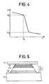
- Fig. 4 represents the resistance characteristics as a function of the temperature of the resistors with a non-linear negative temperature coefficient.
- the heating resistors according to the invention therefore have the advantage of having a high value at ordinary temperature and then, when they have been programmed and the underlying resistance layer has heated the variable resistance layer, they do not have more than a low resistance value, which allows on the one hand to remove diodes in the supply circuit since the other resistors, not programmed, have high values, and on the other hand to dissipate the heat mainly towards paper.
- An improvement to the invention consists in permanently programming a low current through all of the heating resistors so as to maintain them at a constant temperature apart from any programming which is slightly lower than the switching temperature.
- Fig. 5 shows an improvement made to the structure of the heating resistors according to the invention.
- the description of the invention, in fig. 3, was based on the simplest case where a variable resistivity layer 19 is deposited on a single layer with constant resistivity 18. However, it is an improvement to produce a variable resistivity layer 19 on a plurality of layers with constant resistivity, two of which have been represented at 18 and at 20 in FIG. 5.
- variable resistivity layer 19 on a support composed of a plurality of layers from 1 to n, the resistivity of each layer decreasing from layer 1 to layer n.
- each layer is deposited so that only the first layer touches the substrate 15 of the thermal printer head, so as to focus the heat given off in each layer, heat which is greater in one layer than in the previous one, towards the external surface of the thermal resistance, which means that the external surface is the warmest and which modifies the paper used in the thermal printer.
Landscapes
- Electronic Switches (AREA)
Applications Claiming Priority (2)
| Application Number | Priority Date | Filing Date | Title |
|---|---|---|---|
| FR8013967A FR2485796A1 (fr) | 1980-06-24 | 1980-06-24 | Resistance electrique chauffante et tete d'imprimante thermique comportant de telles resistances chauffantes |
| FR8013967 | 1980-06-24 |
Publications (3)
| Publication Number | Publication Date |
|---|---|
| EP0044756A2 EP0044756A2 (fr) | 1982-01-27 |
| EP0044756A3 EP0044756A3 (en) | 1982-02-10 |
| EP0044756B1 true EP0044756B1 (fr) | 1984-08-29 |
Family
ID=9243445
Family Applications (1)
| Application Number | Title | Priority Date | Filing Date |
|---|---|---|---|
| EP81400923A Expired EP0044756B1 (fr) | 1980-06-24 | 1981-06-11 | Résistance électrique chauffante et tête d'imprimante thermique comportant de telles résistances chauffantes |
Country Status (4)
| Country | Link |
|---|---|
| US (1) | US4413170A (enExample) |
| EP (1) | EP0044756B1 (enExample) |
| DE (1) | DE3165766D1 (enExample) |
| FR (1) | FR2485796A1 (enExample) |
Families Citing this family (27)
| Publication number | Priority date | Publication date | Assignee | Title |
|---|---|---|---|---|
| US4484823A (en) * | 1981-01-17 | 1984-11-27 | Fag Kugelfischer Georg Schafer & Co. | Method of determining the boiling point of a liquid |
| JPS5949985A (ja) * | 1982-09-14 | 1984-03-22 | Toshiba Corp | 感熱印字方式 |
| JPS60104351A (ja) * | 1983-11-12 | 1985-06-08 | Victor Co Of Japan Ltd | 感熱転写記録方法 |
| JPS60184858A (ja) * | 1984-03-02 | 1985-09-20 | Hitachi Ltd | サ−マルヘツド |
| US4528539A (en) * | 1984-06-28 | 1985-07-09 | Eaton Corporation | Reduced-size thermal overload relay |
| JPS6186269A (ja) * | 1984-10-04 | 1986-05-01 | Tdk Corp | サ−マルヘツド |
| GB8521931D0 (en) * | 1985-09-04 | 1985-10-09 | British Aerospace | Thermal image producing device |
| FR2591801B1 (fr) * | 1985-12-17 | 1988-10-14 | Inf Milit Spatiale Aeronaut | Boitier d'encapsulation d'un circuit electronique |
| US4947189A (en) * | 1989-05-12 | 1990-08-07 | Eastman Kodak Company | Bubble jet print head having improved resistive heater and electrode construction |
| FR2688629A1 (fr) * | 1992-03-10 | 1993-09-17 | Thomson Csf | Procede et dispositif d'encapsulation en trois dimensions de pastilles semi-conductrices. |
| JPH05275161A (ja) * | 1992-03-26 | 1993-10-22 | Rohm Co Ltd | ライン型加熱体 |
| US5408070A (en) * | 1992-11-09 | 1995-04-18 | American Roller Company | Ceramic heater roller with thermal regulating layer |
| FR2709020B1 (fr) * | 1993-08-13 | 1995-09-08 | Thomson Csf | Procédé d'interconnexion de pastilles semi-conductrices en trois dimensions, et composant en résultant. |
| DE4328791C2 (de) * | 1993-08-26 | 1997-07-17 | Siemens Matsushita Components | Hybrid-Thermistortemperaturfühler |
| BE1007868A3 (nl) * | 1993-12-10 | 1995-11-07 | Koninkl Philips Electronics Nv | Elektrische weerstand. |
| FR2719967B1 (fr) * | 1994-05-10 | 1996-06-07 | Thomson Csf | Interconnexion en trois dimensions de boîtiers de composants électroniques utilisant des circuits imprimés. |
| FR2780808B1 (fr) | 1998-07-03 | 2001-08-10 | Thomson Csf | Dispositif a emission de champ et procedes de fabrication |
| FR2802706B1 (fr) * | 1999-12-15 | 2002-03-01 | 3D Plus Sa | Procede et dispositif d'interconnexion en trois dimensions de composants electroniques |
| FR2875672B1 (fr) * | 2004-09-21 | 2007-05-11 | 3D Plus Sa Sa | Dispositif electronique avec repartiteur de chaleur integre |
| FR2894070B1 (fr) * | 2005-11-30 | 2008-04-11 | 3D Plus Sa Sa | Module electronique 3d |
| FR2895568B1 (fr) * | 2005-12-23 | 2008-02-08 | 3D Plus Sa Sa | Procede de fabrication collective de modules electroniques 3d |
| FR2905198B1 (fr) * | 2006-08-22 | 2008-10-17 | 3D Plus Sa Sa | Procede de fabrication collective de modules electroniques 3d |
| FR2923081B1 (fr) * | 2007-10-26 | 2009-12-11 | 3D Plus | Procede d'interconnexion verticale de modules electroniques 3d par des vias. |
| FR2940521B1 (fr) | 2008-12-19 | 2011-11-11 | 3D Plus | Procede de fabrication collective de modules electroniques pour montage en surface |
| FR2943176B1 (fr) | 2009-03-10 | 2011-08-05 | 3D Plus | Procede de positionnement des puces lors de la fabrication d'une plaque reconstituee |
| US8143559B2 (en) * | 2009-09-01 | 2012-03-27 | Advance Thermo Control, Ltd. | Heating pad with temperature control and safety protection device |
| JP6930696B2 (ja) * | 2016-10-14 | 2021-09-01 | ローム株式会社 | サーマルプリントヘッド |
Family Cites Families (7)
| Publication number | Priority date | Publication date | Assignee | Title |
|---|---|---|---|---|
| US2915724A (en) * | 1957-06-06 | 1959-12-01 | Minnesota Mining & Mfg | Electrical device |
| DE2310641A1 (de) * | 1973-03-01 | 1974-09-19 | Bosch Gmbh Robert | Druckkopf |
| US3973106A (en) * | 1974-11-15 | 1976-08-03 | Hewlett-Packard Company | Thin film thermal print head |
| FR2311410A1 (fr) * | 1975-05-13 | 1976-12-10 | Thomson Csf | Circuit de commutation integre, matrice de commutation et circuits logiques utilisant ledit circuit |
| US4213030A (en) * | 1977-07-21 | 1980-07-15 | Kyoto Ceramic Kabushiki Kaisha | Silicon-semiconductor-type thermal head |
| US4246468A (en) * | 1978-01-30 | 1981-01-20 | Raychem Corporation | Electrical devices containing PTC elements |
| US4206541A (en) * | 1978-06-26 | 1980-06-10 | Extel Corporation | Method of manufacturing thin film thermal print heads |
-
1980
- 1980-06-24 FR FR8013967A patent/FR2485796A1/fr active Granted
-
1981
- 1981-06-11 EP EP81400923A patent/EP0044756B1/fr not_active Expired
- 1981-06-11 DE DE8181400923T patent/DE3165766D1/de not_active Expired
- 1981-06-17 US US06/274,376 patent/US4413170A/en not_active Expired - Fee Related
Also Published As
| Publication number | Publication date |
|---|---|
| DE3165766D1 (en) | 1984-10-04 |
| FR2485796B1 (enExample) | 1983-07-22 |
| US4413170A (en) | 1983-11-01 |
| EP0044756A2 (fr) | 1982-01-27 |
| EP0044756A3 (en) | 1982-02-10 |
| FR2485796A1 (fr) | 1981-12-31 |
Similar Documents
| Publication | Publication Date | Title |
|---|---|---|
| EP0044756B1 (fr) | Résistance électrique chauffante et tête d'imprimante thermique comportant de telles résistances chauffantes | |
| JP3640146B2 (ja) | 保護素子 | |
| EP3384257B1 (fr) | Capteur de motif thermique | |
| FR3054697B1 (fr) | Procede de capture de motif thermique a chauffage optimise des pixels | |
| FR2760931A1 (fr) | Ensemble capteur-dispositif de chauffage | |
| CA2055005A1 (fr) | Circuit electronique controle en temperature | |
| EP0184497B1 (fr) | Sonde de mesure du niveau d'un liquide | |
| FR2671428A1 (fr) | Element fusible realise a partir d'une mince pellicule de fusion deposee sur un substrat. | |
| US6289198B1 (en) | Quick heat roller | |
| EP3120171B1 (fr) | Dispositif optique a membrane deformable a temps de reponse reduit | |
| JP2021136448A (ja) | 自己制限的ヒータ | |
| FR2462013A1 (fr) | Interrupteur thermique temporise | |
| FR2531595A1 (fr) | Dispositif de rechauffage utilisable sur un capteur d'incidence aerodynamique | |
| EP3004823A1 (fr) | Capteur de temperature | |
| FR2504756A1 (fr) | Dispositif de commutation a seuil, dans un systeme comportant une pluralite de composants repartis en deux groupes interdigites | |
| FR2587828A1 (fr) | Appareil et procede permettant d'obtenir une stabilite des rapports resistifs amelioree dans un reseau diviseur resistif | |
| FR2607999A1 (fr) | Ensemble de circuit electronique commande en temperature | |
| FR2588406A1 (fr) | Tete d'enregistrement thermomagnetique et procede de realisation | |
| WO2001056332A1 (fr) | Limiteur de temperature en polymere semi-conducteur et appareil chauffant incorporant un tel limiteur | |
| US4719348A (en) | Optical sensor having heating element to heat amorphous semiconductor film | |
| FR2557728A1 (fr) | Procede de compensation en temperature d'un detecteur photoconducteur | |
| JPS6053448A (ja) | 透光性薄膜ヒ−タ | |
| EP0008275B1 (fr) | Connecteur enfichable comportant un dispositif autorégulé, destiné à stabiliser en température au moins un point de connexion | |
| EP0067752B1 (fr) | Cellule de couplage thermique et enceinte thermostatée comportant une telle cellule | |
| EP0323937A1 (fr) | Structure de support pour capteur de gaz |
Legal Events
| Date | Code | Title | Description |
|---|---|---|---|
| PUAI | Public reference made under article 153(3) epc to a published international application that has entered the european phase |
Free format text: ORIGINAL CODE: 0009012 |
|
| PUAL | Search report despatched |
Free format text: ORIGINAL CODE: 0009013 |
|
| AK | Designated contracting states |
Designated state(s): DE GB IT |
|
| AK | Designated contracting states |
Designated state(s): DE GB IT |
|
| 17P | Request for examination filed |
Effective date: 19820222 |
|
| ITF | It: translation for a ep patent filed | ||
| GRAA | (expected) grant |
Free format text: ORIGINAL CODE: 0009210 |
|
| AK | Designated contracting states |
Designated state(s): DE GB IT |
|
| REF | Corresponds to: |
Ref document number: 3165766 Country of ref document: DE Date of ref document: 19841004 |
|
| PLBE | No opposition filed within time limit |
Free format text: ORIGINAL CODE: 0009261 |
|
| STAA | Information on the status of an ep patent application or granted ep patent |
Free format text: STATUS: NO OPPOSITION FILED WITHIN TIME LIMIT |
|
| 26N | No opposition filed | ||
| PGFP | Annual fee paid to national office [announced via postgrant information from national office to epo] |
Ref country code: GB Payment date: 19930520 Year of fee payment: 13 |
|
| PGFP | Annual fee paid to national office [announced via postgrant information from national office to epo] |
Ref country code: DE Payment date: 19930527 Year of fee payment: 13 |
|
| ITTA | It: last paid annual fee | ||
| PG25 | Lapsed in a contracting state [announced via postgrant information from national office to epo] |
Ref country code: GB Effective date: 19940611 |
|
| GBPC | Gb: european patent ceased through non-payment of renewal fee |
Effective date: 19940611 |
|
| PG25 | Lapsed in a contracting state [announced via postgrant information from national office to epo] |
Ref country code: DE Effective date: 19950301 |