EP0042496B1 - Process of forming graded aperture masks - Google Patents
Process of forming graded aperture masks Download PDFInfo
- Publication number
- EP0042496B1 EP0042496B1 EP81103942A EP81103942A EP0042496B1 EP 0042496 B1 EP0042496 B1 EP 0042496B1 EP 81103942 A EP81103942 A EP 81103942A EP 81103942 A EP81103942 A EP 81103942A EP 0042496 B1 EP0042496 B1 EP 0042496B1
- Authority
- EP
- European Patent Office
- Prior art keywords
- openings
- mask
- aperture
- opening
- aperture mask
- Prior art date
- Legal status (The legal status is an assumption and is not a legal conclusion. Google has not performed a legal analysis and makes no representation as to the accuracy of the status listed.)
- Expired
Links
- 238000000034 method Methods 0.000 title claims abstract description 20
- 238000005530 etching Methods 0.000 claims abstract description 21
- 239000000463 material Substances 0.000 claims abstract description 12
- 239000007921 spray Substances 0.000 claims description 6
- 239000003795 chemical substances by application Substances 0.000 claims 1
- 230000003628 erosive effect Effects 0.000 claims 1
- 238000004513 sizing Methods 0.000 abstract 2
- 230000007423 decrease Effects 0.000 description 6
- 230000003247 decreasing effect Effects 0.000 description 4
- 230000002093 peripheral effect Effects 0.000 description 4
- 229920002120 photoresistant polymer Polymers 0.000 description 3
- 230000005540 biological transmission Effects 0.000 description 2
- 230000000694 effects Effects 0.000 description 2
- 238000010894 electron beam technology Methods 0.000 description 2
- 239000002131 composite material Substances 0.000 description 1
- 150000001875 compounds Chemical class 0.000 description 1
- 230000001419 dependent effect Effects 0.000 description 1
- 238000004519 manufacturing process Methods 0.000 description 1
- 239000000203 mixture Substances 0.000 description 1
- 230000004048 modification Effects 0.000 description 1
- 238000012986 modification Methods 0.000 description 1
- 238000005507 spraying Methods 0.000 description 1
- 239000000126 substance Substances 0.000 description 1
Images
Classifications
-
- H—ELECTRICITY
- H01—ELECTRIC ELEMENTS
- H01J—ELECTRIC DISCHARGE TUBES OR DISCHARGE LAMPS
- H01J9/00—Apparatus or processes specially adapted for the manufacture, installation, removal, maintenance of electric discharge tubes, discharge lamps, or parts thereof; Recovery of material from discharge tubes or lamps
- H01J9/02—Manufacture of electrodes or electrode systems
- H01J9/14—Manufacture of electrodes or electrode systems of non-emitting electrodes
- H01J9/142—Manufacture of electrodes or electrode systems of non-emitting electrodes of shadow-masks for colour television tubes
Definitions
- This invention relates generally to television aperture masks and, more specifically, to a process for forming openings of various sizes in a television aperture mask.
- the prior art aperture mask openings have taken many different shapes including round as shown in the aforementioned patents or elongated as shown in the U.S. Patent 3,883,347. While the shape of the opening may vary in different masks, generally, all masks require the open area in the aperture mask to be graduated to accommodate the characteristics of the human eye. That is, if a television picture is to appear uniform in brightness to the human eye, it is necessary to have a television picture where the central area of the television picture is actually brighter than the peripheral area. To obtain a brighter central area the aperture masks are usually made with larger size openings in the centre of the mask and smaller size openings in the periphery of the mask with openings of intermediate sizes located therebetween.
- the use of a constant density of apertures with gradually decreasing size produces an image that appears uniform in brightness the human eye.
- the brightness or open area is a maximum of 100% in the center of the aperture mask, it decreases to a minimum of 70% in the peripheral region of the aperture mask.
- the U.S. Patent 3,652,895 shows an aperture mask having a plurality of rectangular slots or circular openings with the size and pitch of the openings decreasing in size from the center of the mask to the peripheral portion of the mask.
- Fig. 13 of the U.S. Patent 3,652,895 also shows an alternate concept in which instead of varying the aperture size, the space between apertures is increased to thereby decrease the open area on the peripheral regions of the mask.
- the proces of the present invention in contrast eliminates the dependence on the skill of the operator by defining the openings in one side of the photoresist according to a parameter hereinafter referred to as the over-etch factor.
- the present invention comprises a process of forming in a shadow mask a plurality of openings as set forth in claim 1.
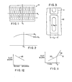
- reference numeral 10 designates an aperture mask having a plurality of apertures 11 therein with C L identifying a vertical center line and H L identifying a horizontal center line through aperture mask 10.
- Fig. 2 is a plot of light transmission or brightness of a television picture as a function of the position of the aperture in the aperture mask.
- the center area of the television tube which corresponds to the center area of the aperture mask has a maximum brightness characteristic which is designated by M x .
- M x maximum brightness characteristic
- Fig. 3 shows an enlarged cone side view of aperture mask 10 having an elongated slot 11 with slot width designated by S w and the cone width designated by C w .
- S w slot width
- C w cone width
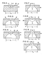
- Fig. 4 shows a sectional side view across an elongated slot of an aperture mask material 16' sandwiched between a grade resist film 15 and a cone side etchant resist film 17.
- the width of opening in grade side resist film 15 is designated by X and the opening in the cone side resist film 17 is designated by X o .
- Identified by reference numeral 20 is a solid line that represents the shape and depth of how a grade side recess would appear if etched for a given time, t.
- the maximum depth of the etched recess would be Do with the top width of the recess slightly larger than the dimension X. It should be pointed out that the size of the etched recess would be larger if etching were allowed to continue for an additional time greater than t and smaller if etching were permitted for a time less than t.
- Fig. 5 shows an identical aperture mask material 16 with grade side resist film 15 and cone side resist film 17.
- Identified by reference numeral 21 is a solid line that represents the shape and depth of how a cone side etched recess would appear if etched for the same time, t, as the grade side recess.
- dimension X o is much larger than X
- the size and shape of the cone side recess is much larger as is the depth of recess 0,.
- the size and shape of the recess will be different even though other parameters such as etchant temperature or Baume are held constant.
- Fig. 6 is a composite drawing showing the theoretical overlap of the recess profiles that are separately achieved when respectively etching the first and second side of the mask, as in Figs. 4 and 5, without submitting the other side to etching.
- the bottom of the projected recess regions extended past each other.
- the distance that each of the recess region extend beyond each other is designated by "a” and is herein defined as the over-etch factor.
- the over- etch factor is not actual over-etching but an indication of how much the projected recess region extends beyond each other.
- the actual etched openings through the material would be defined by the outer portions of solid lines 20 and 21. However, the actual size and shape of the openings is shown in Fig. 7.
- Fig. 7 the actual size and shape of the openings is shown in Fig. 7.
- FIG. 7 shows that the actual etched openings are somewhat larger, even though the etching time, t, for both sides is the same.
- the enlargement is produced by the greater availability of etchant in the localized region due to flow-through of etchant after the breakthrough, with breakthrough defined as the condition when an article is etched completely through from both sides.
- Fig. 11 shows slot width plotted as a function of time.
- the solid line 30 represents how the slot width gradually increases as a function of time. As breakthrough occurs there is steep increase in the slope indicating that the slot width is increasing much faster with time. If etching had continued without breakthrough, the increase in slot width would have continued to follow the dashed line 31.
- T B the slot width increases at a more rapid rate with time as designated by curve 32. This phenomenon is principally due to the circulation of fresh etchant through the opening in the aperture mask.
- the larger slot width would be located in the center of the aperture mask while the narrower slot width is located at the periphery of the mask.
- the slot width Sw c could he been obtained by spraying more etchant into the slot of the aperture mask.
- the result of varying the etchant spray rate may be to produce an overetch factor which is approximately twice the projected differential etch factor "a" as shown in Fig. 6.
- the present process utilizes the discovery that by properly controlling the size of the openings in the resist film in relation to the size of the openings in the grade size resist film so as to keep the over-etch factor substantially constant for each aperture, a suitable modification of the slot width can be achieved. In physical terms this means that, whether the apertures are small or large, breakthrough in etching occurs at substantially the same time for all the apertures in the mask.
- Fig. 9 shows the opening in the lower resist designated by X, with the etch factor of "a". It should be noted that for purposes of understanding the invention, the size of the opening in the top resist layer is designated by X and the same in each one of the figures 3-10. However, in practice it is desired to also grade the grade side resist openings.
- Fig. 10 illustrates a larger cone side opening X 2 with the same identical top opening in resist film 15. Note, the difference in the actual side wall shape 25 with the slot width, S W2 less than the slot width Sw i .
- the process of the invention involves first determining a projected etched recess pattern in one side of the mask material followed by determining a second projected etched recess pattern in the opposite side of the material.
- the overlap distance i.e., the over-etch factor
- the opening in the cone side resist layer is selected so the over-etch factor is kept constant.
- Fig. 12 there is shown slot width in the aperture mask plotted as a function of the size of the resist opening on one side of the mask.
- the opening in the opposite side of the resist varies in accordance with a predetermined manner.
- Numeral 33 identifies a curve for a constant over-etch factor. Curve 33 may be determined experimentally. Once the relationship between slot width and resist opening is known, for a constant over-etch factor, one can go to curve 33 and determine the size of the opening to be formed in an aperture mask by locating the size of the resist opening that corresponds to the desired slot width. It should be understood that the relationship between the slot width and the resist openings will vary as other parameters are altered; however, as long as other parameters remain constant there is a definite relationship that enables one to obtain the proper slot width by merely selecting the proper size resist opening.
- the summation of 0 0 +0 should preferably be about 1.3 times the aperture mask thickness, which means that "a" is approximately 30% of the aperture mask thickness. Under these conditions one normally obtains 60% etch- through from the grade side and 70% from the cone side.
- the values chosen depend primarily on the type of article being made and can be varied in accordance with the type of article desired.
Landscapes
- Engineering & Computer Science (AREA)
- Manufacturing & Machinery (AREA)
- ing And Chemical Polishing (AREA)
- Crystals, And After-Treatments Of Crystals (AREA)
- Electrodes For Cathode-Ray Tubes (AREA)
- Particle Formation And Scattering Control In Inkjet Printers (AREA)
- Manufacture Or Reproduction Of Printing Formes (AREA)
Priority Applications (1)
| Application Number | Priority Date | Filing Date | Title |
|---|---|---|---|
| AT81103942T ATE16658T1 (de) | 1980-06-19 | 1981-05-22 | Verfahren zur herstellung abgestufter lochmasken. |
Applications Claiming Priority (2)
| Application Number | Priority Date | Filing Date | Title |
|---|---|---|---|
| US161062 | 1980-06-19 | ||
| US06/161,062 US4303466A (en) | 1980-06-19 | 1980-06-19 | Process of forming graded aperture masks |
Publications (2)
| Publication Number | Publication Date |
|---|---|
| EP0042496A1 EP0042496A1 (en) | 1981-12-30 |
| EP0042496B1 true EP0042496B1 (en) | 1985-11-21 |
Family
ID=22579654
Family Applications (1)
| Application Number | Title | Priority Date | Filing Date |
|---|---|---|---|
| EP81103942A Expired EP0042496B1 (en) | 1980-06-19 | 1981-05-22 | Process of forming graded aperture masks |
Country Status (6)
| Country | Link |
|---|---|
| US (1) | US4303466A (cg-RX-API-DMAC7.html) |
| EP (1) | EP0042496B1 (cg-RX-API-DMAC7.html) |
| JP (1) | JPS5730236A (cg-RX-API-DMAC7.html) |
| AT (1) | ATE16658T1 (cg-RX-API-DMAC7.html) |
| CA (1) | CA1136025A (cg-RX-API-DMAC7.html) |
| DE (1) | DE3172964D1 (cg-RX-API-DMAC7.html) |
Families Citing this family (14)
| Publication number | Priority date | Publication date | Assignee | Title |
|---|---|---|---|---|
| JPS56139676A (en) * | 1980-04-02 | 1981-10-31 | Toshiba Corp | Method and apparatus for etching metal sheet |
| US4596629A (en) * | 1980-05-12 | 1986-06-24 | Bmc Industries, Inc. | Television picture tubes |
| US4353948A (en) * | 1980-05-12 | 1982-10-12 | Buckbee-Mears Company | Hole technology |
| JPS6070185A (ja) * | 1983-09-26 | 1985-04-20 | Toshiba Corp | シヤドウマスクの製造方法 |
| SU1461377A3 (ru) * | 1984-05-25 | 1989-02-23 | Рка Корпорейшн (Фирма) | Цветной кинескоп |
| US4743795A (en) * | 1984-07-13 | 1988-05-10 | Bmc Industries, Inc. | Multi-graded aperture masks |
| US4632726A (en) * | 1984-07-13 | 1986-12-30 | Bmc Industries, Inc. | Multi-graded aperture mask method |
| US4859549A (en) * | 1987-03-12 | 1989-08-22 | Sony Corporation | Method of forming a fluorescent screen for a color CRT |
| EP0476664B1 (en) * | 1990-09-20 | 1995-07-05 | Dainippon Screen Mfg. Co., Ltd. | Method of forming small through-holes in thin metal plate |
| JP3282347B2 (ja) * | 1993-09-07 | 2002-05-13 | ソニー株式会社 | エッチング法、色選別機構及びその作製方法、並びに、陰極線管 |
| US5484074A (en) * | 1994-05-03 | 1996-01-16 | Bmc Industries, Inc. | Method for manufacturing a shadow mask |
| JP3327246B2 (ja) * | 1999-03-25 | 2002-09-24 | 富士ゼロックス株式会社 | インクジェット記録ヘッド及びその製造方法 |
| DK2516421T3 (en) | 2009-12-23 | 2016-11-28 | Bayer Ip Gmbh | New process for the preparation of 4-aminobut-2-enoliden starting from 4-alkoxyfuran-2 (5H) -one or 4-arylalkoxyfuran-2- (5H) -one |
| CN112103403B (zh) * | 2016-02-16 | 2023-09-05 | Lg伊诺特有限公司 | 金属板、沉积用掩模及其制造方法 |
Family Cites Families (12)
| Publication number | Priority date | Publication date | Assignee | Title |
|---|---|---|---|---|
| US3517921A (en) * | 1968-05-21 | 1970-06-30 | Pitney Bowes Inc | Combined copy paper pre-feed and timing mechanism for copying machines |
| US3652895A (en) * | 1969-05-23 | 1972-03-28 | Tokyo Shibaura Electric Co | Shadow-mask having graduated rectangular apertures |
| US3679500A (en) * | 1970-08-07 | 1972-07-25 | Dainippon Screen Mfg | Method for forming perforations in metal sheets by etching |
| US3663997A (en) * | 1970-09-30 | 1972-05-23 | Rca Corp | Method for making a kinescope comprising production and treatment of a temporary mask |
| JPS4828950A (cg-RX-API-DMAC7.html) * | 1971-08-21 | 1973-04-17 | ||
| JPS4838054A (cg-RX-API-DMAC7.html) * | 1971-09-16 | 1973-06-05 | ||
| US3788912A (en) * | 1971-11-10 | 1974-01-29 | Buckbee Mears Co | System suitable for controlling etching without the aid of an etchant resistant |
| US3909656A (en) * | 1974-05-02 | 1975-09-30 | Zenith Radio Corp | Layered, one-sided etched color selection electrode |
| JPS511511A (en) * | 1974-06-26 | 1976-01-08 | Matsushita Electric Industrial Co Ltd | Denkikogakukokao jusuru jiki |
| US3971682A (en) * | 1974-07-11 | 1976-07-27 | Buckbee-Mears Company | Etching process for accurately making small holes in thick materials |
| US3929532A (en) * | 1974-07-17 | 1975-12-30 | Rca Corp | Method for etching apertured work piece |
| US4126510A (en) * | 1977-10-06 | 1978-11-21 | Rca Corporation | Etching a succession of articles from a strip of sheet metal |
-
1980
- 1980-06-19 US US06/161,062 patent/US4303466A/en not_active Expired - Lifetime
-
1981
- 1981-05-05 CA CA000376899A patent/CA1136025A/en not_active Expired
- 1981-05-22 AT AT81103942T patent/ATE16658T1/de not_active IP Right Cessation
- 1981-05-22 EP EP81103942A patent/EP0042496B1/en not_active Expired
- 1981-05-22 DE DE8181103942T patent/DE3172964D1/de not_active Expired
- 1981-06-19 JP JP9517881A patent/JPS5730236A/ja active Granted
Also Published As
| Publication number | Publication date |
|---|---|
| DE3172964D1 (en) | 1986-01-02 |
| ATE16658T1 (de) | 1985-12-15 |
| JPS6246940B2 (cg-RX-API-DMAC7.html) | 1987-10-05 |
| EP0042496A1 (en) | 1981-12-30 |
| US4303466A (en) | 1981-12-01 |
| JPS5730236A (en) | 1982-02-18 |
| CA1136025A (en) | 1982-11-23 |
Similar Documents
| Publication | Publication Date | Title |
|---|---|---|
| US4303466A (en) | Process of forming graded aperture masks | |
| DE2930290A1 (de) | Verfahren zum herstellen eines gegenstandes | |
| JPS6160889A (ja) | シヤドウマスクの製造方法 | |
| EP0137366B1 (en) | Method for manufacturing a shadow mask | |
| US4632726A (en) | Multi-graded aperture mask method | |
| US4159177A (en) | Color display tube, method of manufacturing such a display tube having a shadow mask, and reproduction mask for use in such a method | |
| US5484074A (en) | Method for manufacturing a shadow mask | |
| CA1052673A (en) | Method for producing an apertured work piece | |
| FI72212C (fi) | Foerfarande foer framstaellning av ett djuptrycksraster. | |
| US4743795A (en) | Multi-graded aperture masks | |
| US4960659A (en) | Method for preparing a shadow mask for a color picture tube | |
| US5348825A (en) | Method for manufacturing shadow mask and shadow mask manufactured by said method | |
| US4518892A (en) | Television picture tube with aperture mask having recesses therein | |
| US3808071A (en) | Etch-back process | |
| CA1047377A (en) | Etching process for accurately making small holes in thick materials | |
| JP2003502717A (ja) | 半導体製造方法 | |
| EP0402616B1 (en) | Emulsion printing plate relief coatings | |
| US3891491A (en) | Apparatus for re-etching a color cathode ray tube shadow mask | |
| EP0546448B1 (en) | Emulsion printing plates and evacuation channels | |
| JPH05174707A (ja) | アパーチャグリルの製造方法 | |
| US4596629A (en) | Television picture tubes | |
| KR20010024957A (ko) | 브라운관용 섀도우 마스크 | |
| US6413437B1 (en) | Fine featured photo-resist artwork design for chemical milling | |
| JPH1069061A (ja) | 位相反転マスク及びその製造方法 | |
| US5236794A (en) | Emulsion printing plate relief coatings |
Legal Events
| Date | Code | Title | Description |
|---|---|---|---|
| PUAI | Public reference made under article 153(3) epc to a published international application that has entered the european phase |
Free format text: ORIGINAL CODE: 0009012 |
|
| AK | Designated contracting states |
Designated state(s): AT BE CH DE FR GB IT LU NL SE |
|
| 17P | Request for examination filed |
Effective date: 19820629 |
|
| GRAA | (expected) grant |
Free format text: ORIGINAL CODE: 0009210 |
|
| AK | Designated contracting states |
Designated state(s): AT BE CH DE FR GB IT LI LU NL SE |
|
| PG25 | Lapsed in a contracting state [announced via postgrant information from national office to epo] |
Ref country code: LI Effective date: 19851121 Ref country code: CH Effective date: 19851121 Ref country code: BE Effective date: 19851121 Ref country code: AT Effective date: 19851121 |
|
| REF | Corresponds to: |
Ref document number: 16658 Country of ref document: AT Date of ref document: 19851215 Kind code of ref document: T |
|
| PG25 | Lapsed in a contracting state [announced via postgrant information from national office to epo] |
Ref country code: SE Effective date: 19851130 |
|
| REF | Corresponds to: |
Ref document number: 3172964 Country of ref document: DE Date of ref document: 19860102 |
|
| ITF | It: translation for a ep patent filed | ||
| RAP2 | Party data changed (patent owner data changed or rights of a patent transferred) |
Owner name: BMC INDUSTRIES, INC. |
|
| REG | Reference to a national code |
Ref country code: CH Ref legal event code: PL |
|
| ET | Fr: translation filed | ||
| RAP2 | Party data changed (patent owner data changed or rights of a patent transferred) |
Owner name: BMC INDUSTRIES, INC. |
|
| PG25 | Lapsed in a contracting state [announced via postgrant information from national office to epo] |
Ref country code: LU Free format text: LAPSE BECAUSE OF NON-PAYMENT OF DUE FEES Effective date: 19860531 |
|
| PLBE | No opposition filed within time limit |
Free format text: ORIGINAL CODE: 0009261 |
|
| STAA | Information on the status of an ep patent application or granted ep patent |
Free format text: STATUS: NO OPPOSITION FILED WITHIN TIME LIMIT |
|
| NLXE | Nl: other communications concerning ep-patents (part 3 heading xe) |
Free format text: IN PAT.BUL.08/86,PAGES 934 AND 941 SHOULD BE MODIFIED INTO:BMC INDUSTRIES, INC. |
|
| 26N | No opposition filed | ||
| ITTA | It: last paid annual fee | ||
| PGFP | Annual fee paid to national office [announced via postgrant information from national office to epo] |
Ref country code: FR Payment date: 20000502 Year of fee payment: 20 |
|
| PGFP | Annual fee paid to national office [announced via postgrant information from national office to epo] |
Ref country code: DE Payment date: 20000503 Year of fee payment: 20 |
|
| PGFP | Annual fee paid to national office [announced via postgrant information from national office to epo] |
Ref country code: GB Payment date: 20000504 Year of fee payment: 20 |
|
| PGFP | Annual fee paid to national office [announced via postgrant information from national office to epo] |
Ref country code: NL Payment date: 20000509 Year of fee payment: 20 |
|
| PG25 | Lapsed in a contracting state [announced via postgrant information from national office to epo] |
Ref country code: GB Free format text: LAPSE BECAUSE OF EXPIRATION OF PROTECTION Effective date: 20010521 |
|
| PG25 | Lapsed in a contracting state [announced via postgrant information from national office to epo] |
Ref country code: NL Free format text: LAPSE BECAUSE OF EXPIRATION OF PROTECTION Effective date: 20010522 |
|
| REG | Reference to a national code |
Ref country code: GB Ref legal event code: PE20 Effective date: 20010521 |
|
| NLV7 | Nl: ceased due to reaching the maximum lifetime of a patent |
Effective date: 20010522 |