EP0037708B1 - Verfahren zur Herstellung eines Musters - Google Patents
Verfahren zur Herstellung eines Musters Download PDFInfo
- Publication number
- EP0037708B1 EP0037708B1 EP81301422A EP81301422A EP0037708B1 EP 0037708 B1 EP0037708 B1 EP 0037708B1 EP 81301422 A EP81301422 A EP 81301422A EP 81301422 A EP81301422 A EP 81301422A EP 0037708 B1 EP0037708 B1 EP 0037708B1
- Authority
- EP
- European Patent Office
- Prior art keywords
- photoresist film
- wavelength
- radiation
- irradiated
- electron beam
- Prior art date
- Legal status (The legal status is an assumption and is not a legal conclusion. Google has not performed a legal analysis and makes no representation as to the accuracy of the status listed.)
- Expired
Links
Images

Classifications
-
- G—PHYSICS
- G03—PHOTOGRAPHY; CINEMATOGRAPHY; ANALOGOUS TECHNIQUES USING WAVES OTHER THAN OPTICAL WAVES; ELECTROGRAPHY; HOLOGRAPHY
- G03F—PHOTOMECHANICAL PRODUCTION OF TEXTURED OR PATTERNED SURFACES, e.g. FOR PRINTING, FOR PROCESSING OF SEMICONDUCTOR DEVICES; MATERIALS THEREFOR; ORIGINALS THEREFOR; APPARATUS SPECIALLY ADAPTED THEREFOR
- G03F7/00—Photomechanical, e.g. photolithographic, production of textured or patterned surfaces, e.g. printing surfaces; Materials therefor, e.g. comprising photoresists; Apparatus specially adapted therefor
- G03F7/70—Microphotolithographic exposure; Apparatus therefor
- G03F7/70425—Imaging strategies, e.g. for increasing throughput or resolution, printing product fields larger than the image field or compensating lithography- or non-lithography errors, e.g. proximity correction, mix-and-match, stitching or double patterning
- G03F7/7045—Hybrid exposures, i.e. multiple exposures of the same area using different types of exposure apparatus, e.g. combining projection, proximity, direct write, interferometric, UV, x-ray or particle beam
-
- G—PHYSICS
- G03—PHOTOGRAPHY; CINEMATOGRAPHY; ANALOGOUS TECHNIQUES USING WAVES OTHER THAN OPTICAL WAVES; ELECTROGRAPHY; HOLOGRAPHY
- G03F—PHOTOMECHANICAL PRODUCTION OF TEXTURED OR PATTERNED SURFACES, e.g. FOR PRINTING, FOR PROCESSING OF SEMICONDUCTOR DEVICES; MATERIALS THEREFOR; ORIGINALS THEREFOR; APPARATUS SPECIALLY ADAPTED THEREFOR
- G03F7/00—Photomechanical, e.g. photolithographic, production of textured or patterned surfaces, e.g. printing surfaces; Materials therefor, e.g. comprising photoresists; Apparatus specially adapted therefor
- G03F7/004—Photosensitive materials
- G03F7/039—Macromolecular compounds which are photodegradable, e.g. positive electron resists
-
- G—PHYSICS
- G03—PHOTOGRAPHY; CINEMATOGRAPHY; ANALOGOUS TECHNIQUES USING WAVES OTHER THAN OPTICAL WAVES; ELECTROGRAPHY; HOLOGRAPHY
- G03F—PHOTOMECHANICAL PRODUCTION OF TEXTURED OR PATTERNED SURFACES, e.g. FOR PRINTING, FOR PROCESSING OF SEMICONDUCTOR DEVICES; MATERIALS THEREFOR; ORIGINALS THEREFOR; APPARATUS SPECIALLY ADAPTED THEREFOR
- G03F7/00—Photomechanical, e.g. photolithographic, production of textured or patterned surfaces, e.g. printing surfaces; Materials therefor, e.g. comprising photoresists; Apparatus specially adapted therefor
- G03F7/20—Exposure; Apparatus therefor
- G03F7/2022—Multi-step exposure, e.g. hybrid; backside exposure; blanket exposure, e.g. for image reversal; edge exposure, e.g. for edge bead removal; corrective exposure
-
- H—ELECTRICITY
- H05—ELECTRIC TECHNIQUES NOT OTHERWISE PROVIDED FOR
- H05K—PRINTED CIRCUITS; CASINGS OR CONSTRUCTIONAL DETAILS OF ELECTRIC APPARATUS; MANUFACTURE OF ASSEMBLAGES OF ELECTRICAL COMPONENTS
- H05K3/00—Apparatus or processes for manufacturing printed circuits
- H05K3/0073—Masks not provided for in groups H05K3/02 - H05K3/46, e.g. for photomechanical production of patterned surfaces
- H05K3/0082—Masks not provided for in groups H05K3/02 - H05K3/46, e.g. for photomechanical production of patterned surfaces characterised by the exposure method of radiation-sensitive masks
-
- H—ELECTRICITY
- H05—ELECTRIC TECHNIQUES NOT OTHERWISE PROVIDED FOR
- H05K—PRINTED CIRCUITS; CASINGS OR CONSTRUCTIONAL DETAILS OF ELECTRIC APPARATUS; MANUFACTURE OF ASSEMBLAGES OF ELECTRICAL COMPONENTS
- H05K3/00—Apparatus or processes for manufacturing printed circuits
- H05K3/02—Apparatus or processes for manufacturing printed circuits in which the conductive material is applied to the surface of the insulating support and is thereafter removed from such areas of the surface which are not intended for current conducting or shielding
- H05K3/06—Apparatus or processes for manufacturing printed circuits in which the conductive material is applied to the surface of the insulating support and is thereafter removed from such areas of the surface which are not intended for current conducting or shielding the conductive material being removed chemically or electrolytically, e.g. by photo-etch process
- H05K3/061—Etching masks
- H05K3/064—Photoresists
-
- Y—GENERAL TAGGING OF NEW TECHNOLOGICAL DEVELOPMENTS; GENERAL TAGGING OF CROSS-SECTIONAL TECHNOLOGIES SPANNING OVER SEVERAL SECTIONS OF THE IPC; TECHNICAL SUBJECTS COVERED BY FORMER USPC CROSS-REFERENCE ART COLLECTIONS [XRACs] AND DIGESTS
- Y10—TECHNICAL SUBJECTS COVERED BY FORMER USPC
- Y10S—TECHNICAL SUBJECTS COVERED BY FORMER USPC CROSS-REFERENCE ART COLLECTIONS [XRACs] AND DIGESTS
- Y10S430/00—Radiation imagery chemistry: process, composition, or product thereof
- Y10S430/143—Electron beam
Definitions
- the present invention relates to a method of forming patterns, and more specifically to a method of forming fine patterns such as required in semiconductor devices and magnetic bubble memory elements.
- the wavelengths of electron beams are so much shorter than the wavelengths of ultraviolet light that adverse effects caused by interference and diffraction can be neglected, and very fine patterns can be formed while maintaining precision.
- a pattern is described by the electron beam on a resist film applied onto a workpiece (such as a metal film, silicon oxide film or the like), and is subjected to developing to form a desired resist pattern.
- a workpiece such as a metal film, silicon oxide film or the like
- the underlying workpiece is processed by etching to form a pattern in the workpiece.
- wet etching employing an etching solution, however, it is difficult to accurately form fine patterns smaller than about 1 urn. Therefore, a dry etching method is employed, utilizing sputtering properties of low-temperature plasma or highspeed ions. Therefore, the resist film exposed to the electron beam must have high resolving power, and must not be deteriorated or deformed by the dry etching.
- PMMA polymethyl methacrylate which is a positive-type resist for exposure to electron beams
- a PSG film phosphorus glass film
- C 4 F s and helium gases with the PMMA as a mask
- abnormal wrinkles develop on the whole surfaces of the resist film. Namely, the pattern is deformed by the wrinkles, and it becomes difficult to obtain a good resist pattern.
- PGMA polyglycidyl methacrylate
- PGMA polyglycidyl methacrylate
- Heat treatment also occurs in the methods of FR-A-2316625 and EP-A-0021719 (the latter published after the priority date of the present invention).
- the photoresist film is exposed to an electron beam' and then heat treated prior to exposure to ultra-violet light.
- the heat treatment causes a reaction in the predetermined regions exposed to the electron beam which makes the predetermined regions insoluble.
- the present invention proposes a method of forming a pattern comprising:
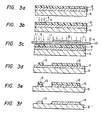
- a positive-type photoresist AZ1350J (trade name, a produce of Shippley Co., U.S.A.) is applied as a resist film 1 to a thickness of 0.6 to 1.0 Ilm on the surface of a film (metal film, insulating film or the like on a semiconductor substrate) 2 on which a pattern is to be formed.
- the resist film 1 is heat-treated at 90°C for 30 minutes (this heat treatment is referred to as pre-bake in this specification).
- the resist film 1 is irradiated with an electron beam 3 to describe a desired pattern.
- the optimum dosage of electrons will be from 1 x 10- 5 to 5 x 10- 5 C/ c m2 .
- the resist film 1 irradiated with the electron beam is then exposed over its whole surface to ultraviolet light 4 as shown in Fig. 1 c.
- ultraviolet light 4 In this case, an ultra-high pressure mercury lamp is used as the source of light, and the exposure is effected at an intensity of 7 to 8 mJ/cm 2 over 10 to 30 seconds.
- the regions irradiated only with ultraviolet light 4 exhibit markedly increased solubility.
- the regions irradiated with the electron beam 3 in the previous step may thereby exhibit slightly increased solubility.
- photosensitive radicals possessed by the photoresist film 1 are destroyed by the electron beam, such regions do not develop photochemical reaction when they are irradiated with ultraviolet light 4 in the above step. Therefore, the solubility of such regions is not increased in this step.
- the increase in solubility of the positive-type photoresist caused by the irradiation with ultra- violet light is far greater than the increase in solubility caused by the irradiation with the electron beam. Accordingly, there are formed regions having a greatly increased solubility caused by the irradiation with the ultraviolet light 4, and regions having slightly increased solubility caused by the irradiation with the electron beam.
- the photoresist film 1 is then subjected to a heat-treatment at 100° to 130°C for 30 minutes (this heat treatment is referred to as an after-bake in this specification), and is then developed. Namely, the regions irradiated with the ultraviolet light 4 only are dissolved and removed. The regions irradiated with both the electron beam 3 and ultraviolet light 4, however, are not removed but remain. A resist pattern 5 is thus formed as shown in Fig. 1d.
- the developing is effected by immersing the film in a solution of organic ammonium or in an alkali aqueous solution at a solution temperature of 20° to 25°C for 1 to 2 minutes.
- a step of exposing the whole surface of the film to ultraviolet light is added to the ordinary step of treating the resist film with an electron beam. This method makes it possible to accurately form fine resist patterns of a size of smaller than 1 ⁇ m.
- Fig. 2 is a graph of the sensitivity curve of a resist with respect to the electron beam, the resist being obtained by treating the photosensitive resist AZ1350J under the above-mentioned conditions.
- the abscissa represents the dosage of electron beam (C/cm 2 ) and the ordinate represents the ratio of film thickness of the negative-type pattern after developing (thickness of the resist film of the portions irradiated with the electron beam after developing to thickness of the resist film after the pre-bake).
- the resist pattern is formed if the dosage of electron beam is greater than about 1 x 10- 5 C/cm 2 .
- the dosage of electrons should be 1 x 10- 5 to 5 x 10- 5 C/ cm 2 .
- Fig. 3 is a diagram illustrating the steps according to another embodiment of the present invention.
- an aluminum film 7 which is to be processed is formed by a vacuum vaporization method on the surface of a silicon substrate 6, and AZ1350J (trade name, a product of Shippley Co.) is applied as a photoresist film 8 to a thickness of 0.8 um onto the aluminum film 7.
- a desired region 9 in the photoresist film 8 is irradiated with an electron beam 3 as shown in Fig. 3b using an electron-beam lithographic apparatus.
- the electron beam dosage in this case is 3 x 10- 5 coulomb/cm 2 .
- desired regions 11 in the photoresist film 8 and the region 9 irradiated with the electron beam 3 in the above step are selectively irradiated with ultraviolet light 4 using a chromium mask 10.
- the irradiation is effected by using a mercury lamp having an output of 13 mW/ cm 2 as a source of light, for an exposure time of 12 seconds.
- the regions 11 in the photoresist film 8 irradiated with the ultraviolet light 4 exhibit increased solubility, but the regions 12 which are not irradiated with the ultraviolet light do not exhibit an increased solubility.
- the region 9 irradiated with the electron beam 3 in the previous step exhibits slightly increased solubility as a result. However, since the photosensitive radicals have been destroyed by the irradiation with electrons, the solubility of the region 9 is not further increased when it is irradiated with the ultraviolet light 4.
- the positive-type photoresist irradiated with only the ultraviolet light exhibits far greater solubility than the solubility of the portions irradiated with the electron beam. Consequently, there are formed regions 11 having the greatest solubility owing to the irradiation with the ultraviolet light 4 only, the region 9 having slightly increased solubility being irradiated with both the electron beams 3 and ultraviolet light 4, and the region 12 which is irradiated with neither the electron beam nor the ultraviolet light and which exhibits the original solubility.
- the shape of the pattern 13 is determined by the irradiation with electron beams, and the shape of the pattern 14 is determined by the irradiation with ultraviolet light.
- the irradiation with electrons makes it possible to form fine patterns maintaining very high precision. Therefore, the above pattern 13 is suited for forming wirings in the semiconductor devices.
- the pattern formed by the irradiation of ultraviolet light is of lower precision than the pattern formed by the irradiation with the electron beam. Therefore, the pattern 14 is suited for forming scribe lines or bonding pads of semiconductor devices having relatively wide areas and which do not require strict precision for the shapes and sizes.
- Magnetic bubble memory elements and semiconductor integrated circuits contain fine patterns which require very high precision and patterns of relatively large areas which do not require high precision.
- Electron beam lithography helps obtain very high precision. When used for forming patterns of large areas, however, electron beam lithography requires greatly extended periods of time before the patterns are described. When ultraviolet light is employed, on the other hand, the exposure needs be effected one time only, but it is difficult to form fine patterns maintaining precision.
- the patterns can be formed with high precision but requiring greatly extended periods of time. If ultraviolet light only is employed, on the other hand, it is difficult to obtain fine patterns maintaining high precision.
- the present invention was accomplished based on a discovery that the solubility of the positive-type photoresist increases quite differently depending upon whether it is irradiated with an electron beam or ultraviolet light, and that the regions irradiated with the electron beams do not exhibit increased solubility even when it is further irradiated with ultraviolet light. This fact makes the present invention greatly distinguished over the prior art.
- the photosensitive radicals in the positive-type photoresist are substantially destroyed by the irradiation with the electron beam, and the solubility is not increased by the irradiation with the ultraviolet light.
- the intensity of the electron beam to be irradiated must be greater than about 1 x 10- 6 coulomb/cm 2 .
- the intensity of the electron beam is smaller than the above value, the photosensitive radicals are not sufficiently destroyed, and the solubility is increased by the irradiation with ultraviolet light and, hence, the positive-type photoresist is dissolved by the developing and is removed.
- the intensity of the electron beam When the intensity of the electron beam becomes greater than about 1 x 10- 4 coulomb/ cm 2 , on the other hand, it becomes difficult to form fine patterns. Therefore, the intensity of the electron beam should range from about 1 x 10⁻⁶ to 1 x 10 -4 coulomb/cm 2 .
- the ultraviolet light should be irradiated under the conditions in which the positive-type photoresist is ordinarily exposed. For example, good results will be obtained when the mercury lamp having an output of 13 mW is used as a source of light, and the irradiation is continued for 8 seconds.
- the present invention can further be put into practice by using not the AZ-type photoresists but instead using other positive-type photoresists such as OFPR-type photoresists manufactured by Tokyo Ohka Kogyo Co.
- the positive-type photoresists can be developed by using the manufacturer's specified developing liquids under the specified conditions.
- the AZ-type photoresists there can be used MF-312 developer, AZ developer or AZ2401 developer depending upon the kind of the photoresist or the irradiation conditions.
- the developing will be effected under specified conditions of, for example, 23°C for 1 minute.
- the pre-baking effected prior to the irradiation with the electron beam is a widely accepted practice in the art of photolithography, and is advantageous from the standpoint of increasing the adhesiveness by removing solvent.
- the pre-baking should be effected at a temperature of about 60° to 90°C for 20 to 30 minutes.
- the after-baking which is effected after the ultraviolet light have been irradiated but before the developing is effected, is not an essential requirement for the present invention but is very effective from the practical point of view.
- the baking should be effected at a temperature of 100° to 140°C.
- the after-baking is effected at a temperature of lower than 100°C, little adhesiveness is exhibited with respect to the layer that is to be processed.
- the after-baking is effected at a temperature of higher than 140°C, the thermal crosslinking reaction of the polymer proceeds, and the solubility of the whole photoresist film so decreases that it becomes difficult to effect the developing.
- the most desirable temperature ranges from 120° to 130°C.
- the baking (post-baking) effected after the developing is not an indispensable step for the present invention.
- the baking is effected to increase the resistance of the layer when it is to be subjected to etching using the resist pattern as a mask.
- the baking is effected at a temperature of nearly 90° to 100°C.
- the layer to be processed may be subjected to the ordinary wet-type etching using various etching solutions.
- the precision can be greatly increased by dry-type etching such as etching by the reactive sputtering.
- the positive-type photoresist is simply used to form a photoresist pattern. Therefore, the photoresist has very small resistance against dry etching, and it is difficult to subject a metal film or an insulation film to the dry etching by using the positive-type photoresist as a mask.
- the photosensitive radicals are destroyed by the irradiation with the electron beam and the photoresist pattern is hardened to exhibit very great resistance against dry etching. Therefore, it is allowed to effect the , dry etching using the thus hardened photoresist pattern as a mask. According to the present invention, therefore, it is easy to form fine patterns having a line width of 0.5 um. If the beam of electrons is converged more finely, it is possible to form patterns having line widths of 0.2 to 0.3 um.
- the so-called far ultraviolet light having wavelengths smaller than about 300 nm in combination with the above-mentioned ultraviolet light, such that the regions irradiated with the far ultraviolet light are left as photoresist patterns like the case when an electron beam is used.
- a suitable dosage of far ultraviolet light for forming the photoresist patterns will be from about 200 to 300 mW/cm 2 sec.
- photoresist patterns are formed having increased resistance against dry etching. Namely, the photoresist patterns are very suited for processing workpieces by dry etching. Furthermore, the present invention is capable of quickly forming fine patterns which require a high degree of precision together with patterns -which require relatively small precision, and is very effective for the production of magnetic bubble memory elements and semiconductor integrated circuits in which such patterns are contained in a mixed manner.
Landscapes
- Physics & Mathematics (AREA)
- General Physics & Mathematics (AREA)
- Spectroscopy & Molecular Physics (AREA)
- Photosensitive Polymer And Photoresist Processing (AREA)
- Exposure And Positioning Against Photoresist Photosensitive Materials (AREA)
- Exposure Of Semiconductors, Excluding Electron Or Ion Beam Exposure (AREA)
Claims (11)
dadurch gekennzeichnet,
Applications Claiming Priority (4)
| Application Number | Priority Date | Filing Date | Title |
|---|---|---|---|
| JP42021/80 | 1980-04-02 | ||
| JP4202180A JPS56140345A (en) | 1980-04-02 | 1980-04-02 | Formation of pattern |
| JP8662680A JPS5712522A (en) | 1980-06-27 | 1980-06-27 | Forming method of pattern |
| JP86626/80 | 1980-06-27 |
Publications (3)
| Publication Number | Publication Date |
|---|---|
| EP0037708A2 EP0037708A2 (de) | 1981-10-14 |
| EP0037708A3 EP0037708A3 (en) | 1982-06-02 |
| EP0037708B1 true EP0037708B1 (de) | 1986-07-30 |
Family
ID=26381665
Family Applications (1)
| Application Number | Title | Priority Date | Filing Date |
|---|---|---|---|
| EP81301422A Expired EP0037708B1 (de) | 1980-04-02 | 1981-04-01 | Verfahren zur Herstellung eines Musters |
Country Status (3)
| Country | Link |
|---|---|
| US (1) | US4403151A (de) |
| EP (1) | EP0037708B1 (de) |
| DE (1) | DE3175019D1 (de) |
Families Citing this family (20)
| Publication number | Priority date | Publication date | Assignee | Title |
|---|---|---|---|---|
| US4407695A (en) * | 1981-12-31 | 1983-10-04 | Exxon Research And Engineering Co. | Natural lithographic fabrication of microstructures over large areas |
| JPS5968928A (ja) * | 1982-10-13 | 1984-04-19 | Pioneer Electronic Corp | 半導体装置の製造方法 |
| US4702995A (en) * | 1984-08-24 | 1987-10-27 | Nec Corporation | Method of X-ray lithography |
| US4595649A (en) * | 1985-02-19 | 1986-06-17 | Allied Corporation | Glassy TiO2 polymer films as electron beam charge dissipation layers |
| JPS62160981A (ja) * | 1986-01-08 | 1987-07-16 | Mitsubishi Heavy Ind Ltd | 石油タンカ−の改造法 |
| US4931380A (en) * | 1985-07-18 | 1990-06-05 | Microsi, Inc. | Pre-exposure method for increased sensitivity in high contrast resist development of positive working diazo ketone photoresist |
| JPS63185022A (ja) * | 1987-01-27 | 1988-07-30 | Fujitsu Ltd | パタ−ン形成方法 |
| US4772539A (en) * | 1987-03-23 | 1988-09-20 | International Business Machines Corporation | High resolution E-beam lithographic technique |
| US5186788A (en) * | 1987-07-23 | 1993-02-16 | Matsushita Electric Industrial Co., Ltd. | Fine pattern forming method |
| US4847183A (en) * | 1987-09-09 | 1989-07-11 | Hewlett-Packard Company | High contrast optical marking method for polished surfaces |
| JP2544006B2 (ja) * | 1990-06-14 | 1996-10-16 | 株式会社東芝 | 半導体装置の製造方法 |
| US5916733A (en) * | 1995-12-11 | 1999-06-29 | Kabushiki Kaisha Toshiba | Method of fabricating a semiconductor device |
| JP3816006B2 (ja) * | 2002-01-16 | 2006-08-30 | 松下電器産業株式会社 | パターン形成方法 |
| WO2003071587A1 (en) * | 2002-02-15 | 2003-08-28 | University Of Delaware | Process for making photonic crystal circuits using an electron beam and ultraviolet lithography combination |
| AU2003269996A1 (en) * | 2002-08-26 | 2004-03-11 | University Of Delaware | Method for fabricating optical devices in photonic crystal structures |
| MXPA05005102A (es) * | 2002-12-05 | 2005-09-30 | Delgado Acarreta Raul | Dispositivo para contar. |
| DE10350705A1 (de) * | 2003-10-30 | 2005-01-27 | Infineon Technologies Ag | Verfahren zur Herstellung einer integrierten Halbleiterschaltung |
| DE102006053074B4 (de) * | 2006-11-10 | 2012-03-29 | Qimonda Ag | Strukturierungsverfahren unter Verwendung chemisch verstärkter Fotolacke und Belichtungsvorrichtung |
| DE102009045114B4 (de) | 2009-09-29 | 2017-01-05 | Universität Leipzig | Verfahren zur nasschemischen Strukturierung von supraleitenden, ferromagnetischen oder ferroelektrischen Oxiden und dessen Verwendung |
| JP2015046459A (ja) * | 2013-08-28 | 2015-03-12 | ソニー株式会社 | エッチング方法、電子デバイスの製造方法および偏光板の製造方法 |
Family Cites Families (6)
| Publication number | Priority date | Publication date | Assignee | Title |
|---|---|---|---|---|
| DE2529054C2 (de) * | 1975-06-30 | 1982-04-29 | Ibm Deutschland Gmbh, 7000 Stuttgart | Verfahren zur Herstellung eines zur Vorlage negativen Resistbildes |
| DE2543553A1 (de) * | 1975-09-30 | 1977-03-31 | Licentia Gmbh | Verfahren zur herstellung einer aetzmaske |
| US4099062A (en) * | 1976-12-27 | 1978-07-04 | International Business Machines Corporation | Electron beam lithography process |
| JPS5596942A (en) * | 1979-01-19 | 1980-07-23 | Matsushita Electric Ind Co Ltd | Method and apparatus for producing minute pattern |
| JPS587054B2 (ja) * | 1979-06-18 | 1983-02-08 | 富士通株式会社 | レジスト・パタ−ン形成法 |
| DE2927242A1 (de) * | 1979-07-05 | 1981-01-08 | Siemens Ag | Korpuskel- oder roentgenlithografisches verfahren zur strukturerzeugung |
-
1981
- 1981-04-01 DE DE8181301422T patent/DE3175019D1/de not_active Expired
- 1981-04-01 EP EP81301422A patent/EP0037708B1/de not_active Expired
- 1981-04-02 US US06/250,217 patent/US4403151A/en not_active Expired - Fee Related
Also Published As
| Publication number | Publication date |
|---|---|
| EP0037708A3 (en) | 1982-06-02 |
| DE3175019D1 (en) | 1986-09-04 |
| EP0037708A2 (de) | 1981-10-14 |
| US4403151A (en) | 1983-09-06 |
Similar Documents
| Publication | Publication Date | Title |
|---|---|---|
| EP0037708B1 (de) | Verfahren zur Herstellung eines Musters | |
| US5648198A (en) | Resist hardening process having improved thermal stability | |
| US6117622A (en) | Controlled shrinkage of photoresist | |
| US6337175B1 (en) | Method for forming resist pattern | |
| EP0907105B1 (de) | Verfahren zur Herstellung einer Fotomaske mit einer Phasenschieberschicht | |
| US7851136B2 (en) | Stabilization of deep ultraviolet photoresist | |
| KR19990072848A (ko) | 포토레지스트막및그의패턴형성방법 | |
| US6656646B2 (en) | Fabrication method of semiconductor integrated circuit device | |
| US5885756A (en) | Methods of patterning a semiconductor wafer having an active region and a peripheral region, and patterned wafers formed thereby | |
| JP3310202B2 (ja) | レジストパターンの形成方法 | |
| EP0021719A2 (de) | Verfahren zur Herstellung negativer Resistbilder und Resistbilder | |
| JP3373748B2 (ja) | 半導体装置の製造方法 | |
| EP0030117B1 (de) | Verfahren zum Formen einer Öffnung in einem negativen Resistfilm | |
| JPS6150377B2 (de) | ||
| US5928814A (en) | Photomask controlling transmissivity by using an impurity-containing film formed on a transparent substrate | |
| KR100278917B1 (ko) | 반도체 소자의 콘택 마스크 제조방법 | |
| JPS61116838A (ja) | レジストパタ−ン形成方法 | |
| JPH0544169B2 (de) | ||
| KR100372652B1 (ko) | 반도체소자의미세콘택홀형성방법 | |
| JPS6156867B2 (de) | ||
| KR0151228B1 (ko) | 고립된 다수의 패턴을 형성하기 위한 포토마스크 | |
| JP3722597B2 (ja) | 水溶性ポリマーの塗布方法及びパターン形成方法 | |
| JPH0562894A (ja) | 微細パターン形成方法 | |
| KR100187370B1 (ko) | 반도체장치의 패턴형성방법 | |
| KR19990012266A (ko) | 포토 마스크의 리페어 방법 |
Legal Events
| Date | Code | Title | Description |
|---|---|---|---|
| PUAI | Public reference made under article 153(3) epc to a published international application that has entered the european phase |
Free format text: ORIGINAL CODE: 0009012 |
|
| 17P | Request for examination filed |
Effective date: 19810611 |
|
| AK | Designated contracting states |
Designated state(s): DE FR GB NL |
|
| RBV | Designated contracting states (corrected) |
Designated state(s): DE FR GB NL |
|
| PUAL | Search report despatched |
Free format text: ORIGINAL CODE: 0009013 |
|
| AK | Designated contracting states |
Designated state(s): DE FR GB NL |
|
| GRAA | (expected) grant |
Free format text: ORIGINAL CODE: 0009210 |
|
| AK | Designated contracting states |
Kind code of ref document: B1 Designated state(s): DE FR GB NL |
|
| ET | Fr: translation filed | ||
| REF | Corresponds to: |
Ref document number: 3175019 Country of ref document: DE Date of ref document: 19860904 |
|
| PLBE | No opposition filed within time limit |
Free format text: ORIGINAL CODE: 0009261 |
|
| STAA | Information on the status of an ep patent application or granted ep patent |
Free format text: STATUS: NO OPPOSITION FILED WITHIN TIME LIMIT |
|
| 26N | No opposition filed | ||
| PGFP | Annual fee paid to national office [announced via postgrant information from national office to epo] |
Ref country code: GB Payment date: 19950322 Year of fee payment: 15 |
|
| PGFP | Annual fee paid to national office [announced via postgrant information from national office to epo] |
Ref country code: FR Payment date: 19950418 Year of fee payment: 15 |
|
| PGFP | Annual fee paid to national office [announced via postgrant information from national office to epo] |
Ref country code: NL Payment date: 19950430 Year of fee payment: 15 |
|
| PGFP | Annual fee paid to national office [announced via postgrant information from national office to epo] |
Ref country code: DE Payment date: 19950626 Year of fee payment: 15 |
|
| PG25 | Lapsed in a contracting state [announced via postgrant information from national office to epo] |
Ref country code: GB Effective date: 19960401 |
|
| PG25 | Lapsed in a contracting state [announced via postgrant information from national office to epo] |
Ref country code: NL Effective date: 19961101 |
|
| GBPC | Gb: european patent ceased through non-payment of renewal fee |
Effective date: 19960401 |
|
| PG25 | Lapsed in a contracting state [announced via postgrant information from national office to epo] |
Ref country code: FR Effective date: 19961227 |
|
| PG25 | Lapsed in a contracting state [announced via postgrant information from national office to epo] |
Ref country code: DE Effective date: 19970101 |
|
| NLV4 | Nl: lapsed or anulled due to non-payment of the annual fee |
Effective date: 19961101 |
|
| REG | Reference to a national code |
Ref country code: FR Ref legal event code: ST |