EP0037103B1 - Halbleiteranordnung - Google Patents
Halbleiteranordnung Download PDFInfo
- Publication number
- EP0037103B1 EP0037103B1 EP81102341A EP81102341A EP0037103B1 EP 0037103 B1 EP0037103 B1 EP 0037103B1 EP 81102341 A EP81102341 A EP 81102341A EP 81102341 A EP81102341 A EP 81102341A EP 0037103 B1 EP0037103 B1 EP 0037103B1
- Authority
- EP
- European Patent Office
- Prior art keywords
- semiconductor
- region
- semiconductor region
- type
- transistor
- Prior art date
- Legal status (The legal status is an assumption and is not a legal conclusion. Google has not performed a legal analysis and makes no representation as to the accuracy of the status listed.)
- Expired
Links
- 239000004065 semiconductor Substances 0.000 title claims description 158
- 239000000758 substrate Substances 0.000 claims description 30
- 239000012535 impurity Substances 0.000 claims description 21
- 230000005669 field effect Effects 0.000 claims 3
- 230000010354 integration Effects 0.000 description 7
- 238000000034 method Methods 0.000 description 6
- 229910052710 silicon Inorganic materials 0.000 description 6
- 239000010703 silicon Substances 0.000 description 6
- XUIMIQQOPSSXEZ-UHFFFAOYSA-N Silicon Chemical compound [Si] XUIMIQQOPSSXEZ-UHFFFAOYSA-N 0.000 description 5
- 238000009413 insulation Methods 0.000 description 5
- 229910052751 metal Inorganic materials 0.000 description 4
- 239000002184 metal Substances 0.000 description 4
- 230000006870 function Effects 0.000 description 3
- 230000003068 static effect Effects 0.000 description 3
- 229910052782 aluminium Inorganic materials 0.000 description 2
- XAGFODPZIPBFFR-UHFFFAOYSA-N aluminium Chemical compound [Al] XAGFODPZIPBFFR-UHFFFAOYSA-N 0.000 description 2
- 230000015556 catabolic process Effects 0.000 description 2
- 238000010276 construction Methods 0.000 description 2
- 238000009792 diffusion process Methods 0.000 description 2
- ZOXJGFHDIHLPTG-UHFFFAOYSA-N Boron Chemical compound [B] ZOXJGFHDIHLPTG-UHFFFAOYSA-N 0.000 description 1
- 239000004411 aluminium Substances 0.000 description 1
- 229910052787 antimony Inorganic materials 0.000 description 1
- WATWJIUSRGPENY-UHFFFAOYSA-N antimony atom Chemical compound [Sb] WATWJIUSRGPENY-UHFFFAOYSA-N 0.000 description 1
- 230000005540 biological transmission Effects 0.000 description 1
- 229910052796 boron Inorganic materials 0.000 description 1
- 230000000295 complement effect Effects 0.000 description 1
- 238000004519 manufacturing process Methods 0.000 description 1
- 238000012856 packing Methods 0.000 description 1
- 229910021420 polycrystalline silicon Inorganic materials 0.000 description 1
- 150000003376 silicon Chemical class 0.000 description 1
- 239000007787 solid Substances 0.000 description 1
Images


Classifications
-
- H—ELECTRICITY
- H01—ELECTRIC ELEMENTS
- H01L—SEMICONDUCTOR DEVICES NOT COVERED BY CLASS H10
- H01L27/00—Devices consisting of a plurality of semiconductor or other solid-state components formed in or on a common substrate
- H01L27/02—Devices consisting of a plurality of semiconductor or other solid-state components formed in or on a common substrate including semiconductor components specially adapted for rectifying, oscillating, amplifying or switching and having potential barriers; including integrated passive circuit elements having potential barriers
- H01L27/0203—Particular design considerations for integrated circuits
- H01L27/0214—Particular design considerations for integrated circuits for internal polarisation, e.g. I2L
- H01L27/0218—Particular design considerations for integrated circuits for internal polarisation, e.g. I2L of field effect structures
-
- H—ELECTRICITY
- H01—ELECTRIC ELEMENTS
- H01L—SEMICONDUCTOR DEVICES NOT COVERED BY CLASS H10
- H01L27/00—Devices consisting of a plurality of semiconductor or other solid-state components formed in or on a common substrate
- H01L27/02—Devices consisting of a plurality of semiconductor or other solid-state components formed in or on a common substrate including semiconductor components specially adapted for rectifying, oscillating, amplifying or switching and having potential barriers; including integrated passive circuit elements having potential barriers
- H01L27/04—Devices consisting of a plurality of semiconductor or other solid-state components formed in or on a common substrate including semiconductor components specially adapted for rectifying, oscillating, amplifying or switching and having potential barriers; including integrated passive circuit elements having potential barriers the substrate being a semiconductor body
- H01L27/06—Devices consisting of a plurality of semiconductor or other solid-state components formed in or on a common substrate including semiconductor components specially adapted for rectifying, oscillating, amplifying or switching and having potential barriers; including integrated passive circuit elements having potential barriers the substrate being a semiconductor body including a plurality of individual components in a non-repetitive configuration
- H01L27/07—Devices consisting of a plurality of semiconductor or other solid-state components formed in or on a common substrate including semiconductor components specially adapted for rectifying, oscillating, amplifying or switching and having potential barriers; including integrated passive circuit elements having potential barriers the substrate being a semiconductor body including a plurality of individual components in a non-repetitive configuration the components having an active region in common
- H01L27/0705—Devices consisting of a plurality of semiconductor or other solid-state components formed in or on a common substrate including semiconductor components specially adapted for rectifying, oscillating, amplifying or switching and having potential barriers; including integrated passive circuit elements having potential barriers the substrate being a semiconductor body including a plurality of individual components in a non-repetitive configuration the components having an active region in common comprising components of the field effect type
- H01L27/0711—Devices consisting of a plurality of semiconductor or other solid-state components formed in or on a common substrate including semiconductor components specially adapted for rectifying, oscillating, amplifying or switching and having potential barriers; including integrated passive circuit elements having potential barriers the substrate being a semiconductor body including a plurality of individual components in a non-repetitive configuration the components having an active region in common comprising components of the field effect type in combination with bipolar transistors and diodes, or capacitors, or resistors
- H01L27/0716—Devices consisting of a plurality of semiconductor or other solid-state components formed in or on a common substrate including semiconductor components specially adapted for rectifying, oscillating, amplifying or switching and having potential barriers; including integrated passive circuit elements having potential barriers the substrate being a semiconductor body including a plurality of individual components in a non-repetitive configuration the components having an active region in common comprising components of the field effect type in combination with bipolar transistors and diodes, or capacitors, or resistors in combination with vertical bipolar transistors and diodes, or capacitors, or resistors
Definitions
- the present invention relates to a semiconductor device according to the prior art portion of claim 1.
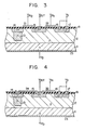
- Fig. 1 is a cross sectional view of a conventional enhancement-depletion (E/D) type inverter circuit device formed by an enhancement type MOS transistor and a depletion type MOS transistor.
- E/D enhancement-depletion
- n-type semiconductor regions 2, 3 and 4 are formed in a p-type semiconductor substrate 1.
- a gate electrode 6 is formed on an insulation layer 5, above the area of the semiconductor substrate 1 between the semiconductor regions 2 and 3.
- a gate electrode 7 is formed on an insulation layer 5 above the area of the semiconductor substrate 1 between the semiconductor regions 3 and 4.
- a donor impurity is ion-implanted in the surface area (channel portion) of the semiconductor substrate 1 between the semiconductor regions 2 and 3 so as to make the threshold voltage negative (e.g., -2V), thus providing a depletion type MOS transistor having the semiconductor region 2 as a drain region and the semiconductor region 3 as a source region.
- An acceptor impurity is ion-implanted in the surface area (channel portion) of the semiconductor substrate 1 between the semiconductor regions 3 and 4 so as to make the threshold voltage positive (e.g., +1V), thus providing an enhancement type MOS transistor having the semiconductor region 3 as a drain region and the semiconductor region 4 as a source region.
- the drain region 2 of the depletion type MOS transistor is connected to a power source voltage terminal VD, and the source region 3 and the gate electrode 6 are commonly connected to the output terminal VOUT.
- the gate electrode 7 of the enhancement type MOS transistor is connected to an input terminal VIN, and the source region 4 is connected to a ground terminal VS1.
- the semiconductor substrate is connected to a ground terminal VS2. An E/D inverter circuit is thus formed.
- the primary object of the present invention to provide a semiconductor device which may be fabricated in a relatively simple manner and which may attain a high integration density.
- a semiconductor device of the present invention has a semiconductor substrate of a first conductivity type, and a semiconductor layer of a second conductivity type opposite to the first conductivity type formed on the substrate.
- this semiconductor layer are formed a first semiconductor region of the first conductivity type, this region having a low impurity concentration and being formed to be deep; and a second semiconductor region formed in a surface area of said semiconductor layer including the surface of said first semiconductor region, said second semiconductor region being of the first conductivity type and having an impurity concentration higher than that of said first semiconductor region and being formed to be shallower than it.
- a power source voltage terminal for supplying a voltage to the second semiconductor region is connected to the semiconductor substrate.
- the power source connecting wiring can be eliminated from the semiconductor layer and a still higher integration density can be attained.
- Fig. 2 shows an example in which the present invention is applied to an E/D inverter circuit device.
- the semiconductor device shown in Fig. 2 has an n-type semiconductor substrate, for example, a silicon substrate 11 in which a donor impurity, e.g., antimony, is doped to a concentration of about 10 15 /cm 3 .
- a donor impurity e.g., antimony
- a p-type semiconductor layer for example, an epitaxial silicon layer 12, to a thickness of, e.g., 10 to 15 ⁇ m.
- an acceptor impurity e.g., boron
- an n-type semiconductor region 13 which is deep (generally 5 to 15 ⁇ m, e.g., 10 , ⁇ m) and which has a low impurity concentration (generally 10 16 to 10 2 °/cm 3 , e.g., 1017/cm3). Although this region 13 is deep, it is generally formed apart from the substrate 11. Thus, the power source voltage may be suitably varied.
- n l- type semiconductor region 14 which has a higher impurity concentration than the semiconductor region 13 (generally 10 19 to 10 21 / cm 3 , e .g., 10 20 /cm 3 ) and which is shallower than the semiconductor region 13 (generally 0.3 to 1.0 ⁇ m, e.g., 0.5 ⁇ m).
- n +- type semiconductor regions 15 and 16 which are of substantially the same impurity concentration as the semiconductor region 14 and which are spaced apart from the semiconductor region 14 and from each other. These semiconductor regions 14, 15 and 16 can be simultaneously formed by diffusion.
- a p +- type semiconductor region 17 is formed in the surface area of the semiconductor layer 12 to establish an ohmic contact.
- Conductive layers (or gate electrodes) 21 and 22 are formed insulated by an insulation layer 18 on areas (channel portions) 19 and 20 of the semiconductor layer 12 between the semiconductor regions 14 and 15 and between the semiconductor regions 15 and 16, respectively.
- a donor impurity and an acceptor impurity are doped in the respective channel portions so as to make the threshold voltage respectively negative (e.g., -2V) and positive (e.g., + 1 V), as in the case of Fig. 1.
- the gate electrode 21 and the source region 15 of the depletion type MOS transistor are commonly connected to the output terminal VOUT.
- the gate electrode 22 of the enhancement type MOS transistor is connected to the input terminal VIN, and the source region 16 is commonly grounded to a grounding terminal VS with the p +- type semiconductor region 17.
- the power source terminal VD is connected directly or through a metal layer 23 to the n-type semiconductor substrate 11, and a power source voltage, e.g., 5V, is applied thereto.
- the mode of operation of such an E/D type inverter circuit device is substantially the same as that shown in Fig. 1.
- the output voltage becomes high level (about 5V) as the input voltage becomes low level (about OV).
- the output voltage becomes low level (about 0V) when the input voltage becomes high level (about 5V).
- the mode of operation of the E/D type inverter circuit device of the present invention shown in Fig. 2 is substantially the same as this, the power source voltage is applied at a different place.
- the power source voltage is not directly applied to the drain region of the depletion type MOS transistor as in the case of the device shown in Fig. 1, but is supplied indirectly (that is, through the p-type semiconductor layer 12 and the n-type semiconductor region 13) from the substrate 11 to the drain region 14. That is to say, an npn type bipolar transistor is formed which has the n-type semiconductor substrate 11 as a collector region, the p-type semiconductor layer 12 as a base region, and the n-type semicn- ductor region 13 as an emitter region, and the power source voltage is supplied to the drain region 14 by turning on this bipolar transistor.
- the breakdown voltage between the n-type semiconductor substrate 11 and the p-type semiconductor layer 12 is lowered.
- a leakage current above the current required to render the circuit operative for inverting operation is applied to the base region under the condition that a voltage substantially corresponding to the power source voltage is being applied.
- the potential of the part to become the base region is raised by the distributed resistance of the semiconductor layer 12 to turn on the npn type transistor.
- the part of the semiconductor layer 12 to become the base region that is, between the semiconductor region 13 and the substrate 11, is made as thin as possible. Then, a punch-through current flows by the power source voltage to induce a voltage across the n-type semiconductor region 13.
- the npn type bipolar transistor may be turned on by selecting the breakdown voltage and the leakage current between the n-type substrate 11 and the p-type layer 12, the thickness of the part of the p-type layer 12 to become the base region, the impurity concentration of the p-type layer and so on, thereby supplying the power source voltage to the drain region of the depletion type MOS transistor.
- the above-mentioned selection may be easily performed by those skilled in the art. A concrete example was described hereinabove.
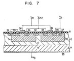
- the present invention may be applied to a complementary MOS device by making the deep semiconductor region formed in the semiconductor layer a well region. Such examples are shown in Figs. 6 and 7.
- the structure shown in Fig. 6 has the n-type silicon substrate 11 and the p-type epitaxial silicon layer 12 formed on its major surface as in the case of the structure of Fig. 2.
- An n-type well region 31 of 8 ⁇ m depth, for example, is formed within the semiconductor layer 12, and the impurity concentration of the surface area thereof is 10 16 / CM 3 , for example.
- An n l- type region 32 is formed as a guard ring for the n-type well region 31 within the surface areas of the n-type well region 31 and the semiconductor layer 12 at the boundary therebetween.
- n-type well region 31 In the surface area of the n-type well region 31 are formed p l- type regions 33 and 34 to be used as the source and drain regions of the p-channel MOS transistor. In the surface area of the semiconductor layer 12 are formed n +- type regions 35 and 36 to be used as the drain and source regions of the n-channel MOS transistor. A p +- type region 37 is formed in the surface of the semiconductor layer 12 to be contiguous with the n +- type region 36.
- Conductive layers (gate electrodes) 38 and 39 are formed on the insulation layer 18, above the area between the p +- type regions 33 and 34 and above the area between the n +- type regions 35 and 36, respectively.
- the p +- type region 37 and the source region 36 of the n-channel MOS transistor are commonly connected to the ground terminal VS.
- the drain region 34 of the p-channel MOS transistor and the drain region 35 of the n-channel MOS transistor are commonly connected to the output terminal VOUT.
- the gate electrode 38 of the p-channel MOS transistor and the gate electrode 39 of the n-channel MOS transistor are commonly connected to the. input terminal VIN.
- the source region 33 of the p-channel MOS transistor and the n +- type region 32 are commonly connected and placed under floating condition.
- the power source voltage terminal VD of, for example, 5V, is connected to the n-type substrate 11 directly or through the metal layer 23.
- the voltage supplied to the power source voltage terminal VD is supplied to the n-type well region by turning on the npn type bipolar transistor having the n-type substrate 11 as a collector region, the p-type semiconductor layer 12 as a base region, and the n-type well region 31 as an emitter region, as has been already described with reference to Fig. 2.
- the structure shown in Fig. 7 is basically the same as that shown in Fig. 6, except that the n +- type regions 35 and 36 are formed in the surface area of a p-type well region 40.
- the resistivity of the p-type semiconductor layer 12 is high (e.g., 100 Q cm). Therefore, it is easier to turn on the npn type bipolar transistor.
- the present invention it is possible to eliminate the power source voltage wiring of metal such as aluminium from the surface of the semiconductor layer, so that a semiconductor device with a higher integration density may be obtained. Furthermore, the process for fabricating this semiconductor device becomes extremely simple since the complex power source wiring may be eliminated by simply forming a semiconductor layer and forming a deep semiconductor region which is low in impurity concentration. In general, with a MOS type LSI, the ratio of the power source wiring area to the chip area is quite large, especially in the case of a memory cell of MOS type static memory. However, according to the present invention, the power source wiring may be eliminated from the surface of the semiconductor layer so that the chip area may be reduced by 20% or more.
- a semiconductor device of opposite conductivity type may be obtained by reversing the conductivity types in the embodiments described above.
- MOS transistor circuits such as NOR gate circuits, NAND gate circuits, transmission gate circuits, buffer circuits and the like.
Landscapes
- Engineering & Computer Science (AREA)
- Power Engineering (AREA)
- Physics & Mathematics (AREA)
- Condensed Matter Physics & Semiconductors (AREA)
- General Physics & Mathematics (AREA)
- Computer Hardware Design (AREA)
- Microelectronics & Electronic Packaging (AREA)
- Metal-Oxide And Bipolar Metal-Oxide Semiconductor Integrated Circuits (AREA)
Claims (19)
Applications Claiming Priority (4)
| Application Number | Priority Date | Filing Date | Title |
|---|---|---|---|
| JP40209/80 | 1980-03-31 | ||
| JP4020980A JPS56137668A (en) | 1980-03-31 | 1980-03-31 | Semiconductor device |
| JP55178941A JPS57103357A (en) | 1980-12-19 | 1980-12-19 | Semiconductor device |
| JP178941/80 | 1980-12-19 |
Publications (2)
| Publication Number | Publication Date |
|---|---|
| EP0037103A1 EP0037103A1 (de) | 1981-10-07 |
| EP0037103B1 true EP0037103B1 (de) | 1984-02-01 |
Family
ID=26379648
Family Applications (1)
| Application Number | Title | Priority Date | Filing Date |
|---|---|---|---|
| EP81102341A Expired EP0037103B1 (de) | 1980-03-31 | 1981-03-27 | Halbleiteranordnung |
Country Status (3)
| Country | Link |
|---|---|
| US (1) | US4476479A (de) |
| EP (1) | EP0037103B1 (de) |
| DE (1) | DE3162083D1 (de) |
Families Citing this family (10)
| Publication number | Priority date | Publication date | Assignee | Title |
|---|---|---|---|---|
| US4757363A (en) * | 1984-09-14 | 1988-07-12 | Harris Corporation | ESD protection network for IGFET circuits with SCR prevention guard rings |
| GB2215123B (en) * | 1988-02-16 | 1990-10-24 | Stc Plc | Improvement in integrated circuits |
| JPH01147854A (ja) * | 1987-12-04 | 1989-06-09 | Nissan Motor Co Ltd | 半導体装置 |
| JP2737334B2 (ja) * | 1989-01-23 | 1998-04-08 | モトローラ・インコーポレーテッド | 電力集積回路用基板電力供給接点 |
| US5293057A (en) * | 1992-08-14 | 1994-03-08 | Micron Technology, Inc. | Electrostatic discharge protection circuit for semiconductor device |
| US6833590B2 (en) * | 2001-01-11 | 2004-12-21 | Renesas Technology Corp. | Semiconductor device |
| JP2002208644A (ja) * | 2001-01-11 | 2002-07-26 | Mitsubishi Electric Corp | 半導体装置 |
| US6624660B2 (en) * | 2001-12-06 | 2003-09-23 | Micron Technology, Inc. | CMOS output driver for semiconductor device and related method for improving latch-up immunity in a CMOS output driver |
| US9379109B1 (en) * | 2012-04-04 | 2016-06-28 | Xilinx, Inc. | Integrated circuit having improved radiation immunity |
| US9236353B2 (en) | 2012-11-27 | 2016-01-12 | Xilinx, Inc. | Integrated circuit having improved radiation immunity |
Family Cites Families (7)
| Publication number | Priority date | Publication date | Assignee | Title |
|---|---|---|---|---|
| US3440503A (en) * | 1967-05-31 | 1969-04-22 | Westinghouse Electric Corp | Integrated complementary mos-type transistor structure and method of making same |
| DE2055662C3 (de) * | 1970-11-12 | 1979-10-18 | Deutsche Itt Industries Gmbh, 7800 Freiburg | Monolithisch integrierte Festkörperschaltung |
| US3758831A (en) * | 1971-06-07 | 1973-09-11 | Motorola Inc | Transistor with improved breakdown mode |
| NL161305C (nl) * | 1971-11-20 | 1980-01-15 | Philips Nv | Werkwijze voor het vervaardigen van een halfgeleiderin- richting. |
| JPS5214383A (en) * | 1975-07-24 | 1977-02-03 | Fujitsu Ltd | Mis-type semiconductor device |
| US4225877A (en) * | 1978-09-05 | 1980-09-30 | Sprague Electric Company | Integrated circuit with C-Mos logic, and a bipolar driver with polysilicon resistors |
| JPS5939904B2 (ja) * | 1978-09-28 | 1984-09-27 | 株式会社東芝 | 半導体装置 |
-
1981
- 1981-03-24 US US06/247,156 patent/US4476479A/en not_active Expired - Lifetime
- 1981-03-27 DE DE8181102341T patent/DE3162083D1/de not_active Expired
- 1981-03-27 EP EP81102341A patent/EP0037103B1/de not_active Expired
Also Published As
| Publication number | Publication date |
|---|---|
| EP0037103A1 (de) | 1981-10-07 |
| DE3162083D1 (en) | 1984-03-08 |
| US4476479A (en) | 1984-10-09 |
Similar Documents
| Publication | Publication Date | Title |
|---|---|---|
| US5780899A (en) | Delta doped and counter doped dynamic threshold voltage MOSFET for ultra-low voltage operation | |
| EP0134432B1 (de) | Komplementäre integrierte Halbleiterschaltung mit Schutzanordnung | |
| JP2001352077A (ja) | Soi電界効果トランジスタ | |
| JPS6278869A (ja) | Esd保護装置 | |
| US5286992A (en) | Low voltage device in a high voltage substrate | |
| JPH06260652A (ja) | 高電圧パワートランジスタおよびその形成方法 | |
| JP2004501501A (ja) | 薄いゲート酸化膜用デカップリング・キャパシタ | |
| US4893164A (en) | Complementary semiconductor device having high switching speed and latchup-free capability | |
| EP0037103B1 (de) | Halbleiteranordnung | |
| EP0031238B1 (de) | Halbleiterspeichervorrichtung | |
| US5592014A (en) | High breakdown voltage semiconductor device | |
| KR860000159B1 (ko) | 반도체 메모리 | |
| US5604369A (en) | ESD protection device for high voltage CMOS applications | |
| JPS61220371A (ja) | 絶縁基板上mos形集積回路装置 | |
| US4956700A (en) | Integrated circuit with high power, vertical output transistor capability | |
| US7538408B2 (en) | Inhibition of parasitic transistor operation in semiconductor device | |
| US5122855A (en) | Semiconductor device with latch-up prevention structure | |
| JP2825038B2 (ja) | 半導体装置 | |
| JPS62136867A (ja) | 半導体装置 | |
| US6537893B2 (en) | Substrate isolated transistor | |
| US4952998A (en) | Integrated circuit with complementary MOS transistors | |
| KR100591125B1 (ko) | 정전기적 방전으로부터의 보호를 위한 게이트 접지 엔모스트랜지스터 | |
| US5936290A (en) | Semiconductor device having an insulated gate field effect transistor and a well spaced from the channel region of the insulated gate field effect transistor | |
| JPS62141754A (ja) | 高耐圧半導体装置 | |
| KR100800252B1 (ko) | 씨모스 공정을 이용한 다이오드 소자의 제조 방법 |
Legal Events
| Date | Code | Title | Description |
|---|---|---|---|
| PUAI | Public reference made under article 153(3) epc to a published international application that has entered the european phase |
Free format text: ORIGINAL CODE: 0009012 |
|
| AK | Designated contracting states |
Designated state(s): DE FR GB NL |
|
| 17P | Request for examination filed |
Effective date: 19811001 |
|
| GRAA | (expected) grant |
Free format text: ORIGINAL CODE: 0009210 |
|
| AK | Designated contracting states |
Designated state(s): DE FR GB NL |
|
| REF | Corresponds to: |
Ref document number: 3162083 Country of ref document: DE Date of ref document: 19840308 |
|
| ET | Fr: translation filed | ||
| RAP2 | Party data changed (patent owner data changed or rights of a patent transferred) |
Owner name: KABUSHIKI KAISHA TOSHIBA |
|
| PLBE | No opposition filed within time limit |
Free format text: ORIGINAL CODE: 0009261 |
|
| STAA | Information on the status of an ep patent application or granted ep patent |
Free format text: STATUS: NO OPPOSITION FILED WITHIN TIME LIMIT |
|
| REG | Reference to a national code |
Ref country code: FR Ref legal event code: CD |
|
| 26N | No opposition filed | ||
| REG | Reference to a national code |
Ref country code: GB Ref legal event code: 746 |
|
| PGFP | Annual fee paid to national office [announced via postgrant information from national office to epo] |
Ref country code: GB Payment date: 19970318 Year of fee payment: 17 |
|
| PGFP | Annual fee paid to national office [announced via postgrant information from national office to epo] |
Ref country code: DE Payment date: 19970404 Year of fee payment: 17 |
|
| PGFP | Annual fee paid to national office [announced via postgrant information from national office to epo] |
Ref country code: FR Payment date: 19980310 Year of fee payment: 18 |
|
| PGFP | Annual fee paid to national office [announced via postgrant information from national office to epo] |
Ref country code: NL Payment date: 19980326 Year of fee payment: 18 |
|
| PG25 | Lapsed in a contracting state [announced via postgrant information from national office to epo] |
Ref country code: GB Free format text: LAPSE BECAUSE OF NON-PAYMENT OF DUE FEES Effective date: 19980327 |
|
| GBPC | Gb: european patent ceased through non-payment of renewal fee |
Effective date: 19980327 |
|
| PG25 | Lapsed in a contracting state [announced via postgrant information from national office to epo] |
Ref country code: DE Free format text: LAPSE BECAUSE OF NON-PAYMENT OF DUE FEES Effective date: 19981201 |
|
| PG25 | Lapsed in a contracting state [announced via postgrant information from national office to epo] |
Ref country code: NL Free format text: LAPSE BECAUSE OF NON-PAYMENT OF DUE FEES Effective date: 19991001 |
|
| PG25 | Lapsed in a contracting state [announced via postgrant information from national office to epo] |
Ref country code: FR Free format text: LAPSE BECAUSE OF NON-PAYMENT OF DUE FEES Effective date: 19991130 |
|
| NLV4 | Nl: lapsed or anulled due to non-payment of the annual fee |
Effective date: 19991001 |
|
| REG | Reference to a national code |
Ref country code: FR Ref legal event code: ST |