EP0036775A2 - Statische Speicherschaltung - Google Patents
Statische Speicherschaltung Download PDFInfo
- Publication number
- EP0036775A2 EP0036775A2 EP81301224A EP81301224A EP0036775A2 EP 0036775 A2 EP0036775 A2 EP 0036775A2 EP 81301224 A EP81301224 A EP 81301224A EP 81301224 A EP81301224 A EP 81301224A EP 0036775 A2 EP0036775 A2 EP 0036775A2
- Authority
- EP
- European Patent Office
- Prior art keywords
- transistors
- potential
- power supply
- memory cells
- cell
- Prior art date
- Legal status (The legal status is an assumption and is not a legal conclusion. Google has not performed a legal analysis and makes no representation as to the accuracy of the status listed.)
- Granted
Links
Images


Classifications
-
- G—PHYSICS
- G11—INFORMATION STORAGE
- G11C—STATIC STORES
- G11C11/00—Digital stores characterised by the use of particular electric or magnetic storage elements; Storage elements therefor
- G11C11/21—Digital stores characterised by the use of particular electric or magnetic storage elements; Storage elements therefor using electric elements
- G11C11/34—Digital stores characterised by the use of particular electric or magnetic storage elements; Storage elements therefor using electric elements using semiconductor devices
- G11C11/40—Digital stores characterised by the use of particular electric or magnetic storage elements; Storage elements therefor using electric elements using semiconductor devices using transistors
- G11C11/41—Digital stores characterised by the use of particular electric or magnetic storage elements; Storage elements therefor using electric elements using semiconductor devices using transistors forming static cells with positive feedback, i.e. cells not needing refreshing or charge regeneration, e.g. bistable multivibrator or Schmitt trigger
- G11C11/413—Auxiliary circuits, e.g. for addressing, decoding, driving, writing, sensing, timing or power reduction
- G11C11/417—Auxiliary circuits, e.g. for addressing, decoding, driving, writing, sensing, timing or power reduction for memory cells of the field-effect type
Definitions
- the present invention relates to a static memory circuit incorporating memory cells of a MOS static type.
- each of the MOS static memory cells comprises a bi-stable flip-flop which uses four transistors per bit. That is, the memory cell comprises a pair of load resistors, a pair of driver transistors which are cross-coupled to each other, and a pair of transfer gate transistors connected to one word line and one bit line pair. In this memory cell, only one of the driver transistors is turned on to correspond to memory data "0" or "1".
- the transfer gate transistors are turned on by changing the potential of the word line so that the data on the driver transistors is transferred to the bit lines. Similarly, in order to write data into the cell, the transfer gate transistors are also turned on by changing the potential of the word line and proper voltages are then applied to the bit lines.
- One conventional static memory circuit of a MOS static type incorporates a large number of such memory cells arranged along rows and columns which are orthogonal to each other.
- the circuit comprises a plurality of word lines each connected to the memory cells belonging to one row, a plurality of pairs of bit lines, each pair connected to the memory cells belonging to one column, and a plurality of pairs of column selection gates each pair connected to one pair of the bit lines. In this case, selection of one cell among the memory cells is effected by selecting one of the word lines and one pair of the bit lines.
- a static memory circuit comprising: a first power supply; a second power supply the potential of which is lower than that of the first power supply; a plurality of word lines; a plurality of pairs of bit lines; a plurality of pairs of column selection gate transistors each pair connected to one of the pairs of bit lines and controlled by column selection signals; a plurality of memory cells each one of which comprises a pair of first loads connected to the first power supply, first and second transistors each having a gate connected to one of the first loads and to a drain of the other, and having a source connected to a source of the other, and third and fourth transistors each having a drain connected to one of the bit lines, a source connected to one of the drains of the first and second transistors and a gate connected to one of said word lines; and a plurality of means, connected to the sources of the first and second transistors of the memory cells and to the second power supply, for setting the potential of the sources of the first and second transistors of a selected one of the memory
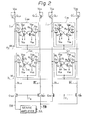
- Each of the memory cells for example, the memory cell C 00 , is connected to one word line WL O which is selected by a row address signal X 0 and to one pair of bit lines BL 0 and BL 0 which are selected by conducting transistors Q BO and Q BO '.
- the transistors Q BO and Q BO ' are column selection gates which are controlled by a column selection signal Y 0 .
- bit lines BL 0 , B L O , BL 1 , BL 1 , ..., BL n-1 , BL n-1 are connected to a power supply V DD through load transistors Q L O ' Q L0 ' Q L1 , Q L1 ', ..., Q L,n-1 , Q L,n-1 ', respectively, and to data bus lines DB and DB connected to a sense amplifier SA through the transistors Q B0 , Q B0 ', Q B1 , Q B1 ', ..., Q B,n-1 , Q B,n-1 ', respectively.
- Fig. 2 is a circuit diagram of the memory cells C 00 , C 01 , C 10 and C 11 of Fig. 1.
- each of the memory cells which are, of course, the same as the other memory cells of Fig. 1, comprises a pair of loads R 1 and R 2 , which are resistors, and a pair of transistors Q 1 and Q 2 cross-coupled to each other, which constitute a flip-flop, and a pair of transfer gate transistors Q 3 and Q 4 .
- a drain and a gate of the transistor Q 1 are connected to a gate and a drain of the transistor Q 2 , respectively.
- the transfer gate transistors Q 3 and Q 4 are connected to the bit lines BL 0 and BL 0 (or BL 1 and BL 1 ), respectively, and the gates of the transistors Q 3 and Q 4 are connected to the word line WL 0 (or WL 1 ), commonly.
- Fig. 2 it should be noted that two gate-drain connected transistors can be used as the load resistors R 1 and R 2 .
- the potential of the row selection signal X 0 that is, the potential of the word line WL 0 is caused to be high by a row driver (not shown), so that the transfer gate transistors Q 3 and Q 4 of the cell C 00 conduct.
- the potentials at nodes N 1 and N 2 of the cell C 00 which are dependent upon the memory data "0" or "1" are transmitted to the bit lines BL 0 and BL O , respectively.
- the transistor Q 1 is conductive, as illustrated in Fig.
- a load current I LO flows from a power supply V DD , through the transistor Q L0 and the transistors Q3 and Q 1 of the cell C 00 to a power supply V SS , so that the potential of the bit line BL 0 is decreased.
- the transistor Q 2 of the cell C 00 is non-conductive, no current flows through the transistor Q L0 ', the transistors Q 4 and Q 2 of the cell C 00 , so that the potential of the bit line BL 0 remains at the same high level which is lower than the power supply V DD by the threshold voltage V th of the transistor Q L0 '.
- the sense amplifier SA when the potential of the column selection signal Y is caused to be high by a column driver (not shown) so that the transistors Q B0 and Q B0 ' are turned on, the difference in potential between the bit lines B LO and B LO , that is, the difference in potential between data bus lines DB and DB is amplified by the sense amplifier SA.
- a hold current I HO flows from the power supply V DD through the resistor R 1 and the transistor Q 1 to the power supply V SS , if the potentials at the nodes N 1 and N 2 thereof are low and high, respectively. Note that such a hold current also flows through both of the selected memory cell C 00 and the half-selected memory cell C 01 ; however, the hold current is much smaller than the load current I LO or I L1 .
- the static memory circuit is of a large scale, which is, for example, 4,096 or 16,384 bits. Therefore, in the case of a 4,096 bit (64 x 64) memory circuit, the above-mentioned load current, which is invalid for the read operation, flows through each of (64-1) half-selected memory cells, while, in the case of a 16,384 bit (128 x 128) memory circuit, such invalid load current flows through each of (128-1) half-selected memory cells, which results in a large power consumption.
- the load current is 0.5 mA per cell
- it is considered to reduce the value of the load current; however, in this case, power for charging the bit lines and the data bus lines DB and DB in the read mode is reduced and accordingly, the read speed is reduced. Therefore, usually, the value of the load current is selected to be an appropriately high so as to increase the read speed.
- hold currents are preferably as small as possible, which is helpful in reducing power consumption, since the number of such non-selected memory cells are much larger than that of half-selected memory cells.
- the hold current has a lower limit; if the hold current is lower than the lower limit, the memory data stored in the cell, that is, the state of the potentials at the nodes N 1 and N 2 can not be maintained.
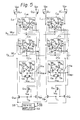
- Fig. 3 is a circuit diagram illustrating an embodiment of the static memory circuit according to the present invention.
- the elements which are the same as those of Fig. 2 are denoted by the same references.
- a common source node N S of the cross-coupled transistors Q 1 and Q 2 is connected not directly to the power supply V SS . That is, the node N S is connected to a reference node N R of a potential setting circuit PS 0 or PS 1 and to a transistor Q 50 or Q 51 .
- Each of the potential setting circuits PS 0 and PS 1 comprises two resistors R 3 and R 4 connected in series and in addition, the transistor Q 50 or Q 51 has a drain connected to the reference node N R of the circuit PS 0 or PS 1 , a source connected to the power supply V SS and a gate for receiving the column selection signal Y 0 or Y 1 .
- the selecting operation of the memory cells is the same as that of Fig. 2. For example, when the potentials of the row selection signals X 0 and X 1 are high and low, respectively, and simultaneously, the potentials of the column selection signals Y 0 and Y 1 are high and low, respectively, the memory cells C 00 , C 01 , C 10 and C 11 are selected, half-selected, non-selected and non-selected, respectively.
- the potential V ref0 that is, the potential at the node N S of the cell C 00 reaches the same level as the power supply V SS . If the transistors Q 1 and Q 2 are conductive and non-conductive, respectively, a load current I LO flows from the power supply V DD through the transistor Q LO , the transistors Q3 and Q 1 of the cell C 00 and the transistor Q 5 to the power supply V SS . At this time, another load current does not flow, since the transistor Q 2 of the cell C 00 is non-conductive.
- the potentials of the bit linesBL and BL 1 become low and high, respectively, and accordingly, the difference in potential therebetween is read out from the data bus lines DB and DB and it is amplified by the sense amplifier SA.
- the load current I LO is selected to be 0.5 mA in the same way as Fig. 2, so that the read speed is never reduced.
- the potential V refl that is, the potential at the node N S reaches the same level as the node N R of the circuit PS I which is determined by the resistors R3 and R4 . Therefore, a load current I L1 flows from the power supply V DD and through the transistor Q L1 , the transistors Q 3 and Q 1 of the cell C 01 and the resistor R 4 of the circuit PS 1 to the power supply V SS .
- the load current I L1 in the half-selected cell C 01 is smaller than the load current I L0 in the selected cell C 00 .
- the load current I L1 can be reduced by selecting the values of the resistors R 3 and R 4 ; however, the load current I L1 should not be so small as to maintain the on- and off-states of the flip-flop of the memory cell C 01 ; that is, maintain the memory data.
- the upper limit of the potential at the node N R is about 3.5 volts.
- the load current I L1 is reduced to be about 0.15 mA and accordingly, current consumptions (0.5 - 0.15) mA x 63 and (0.5 - 0.15) mA x 127 can be saved in a 4,096 bit memory circuit and a 16,384 bit memory circuit, respectively.
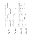
- Figs. 4A through 4D are timing diagrams for explaining the operation of the cell C 00 of Fig. 3.
- the memory cell C 00 has four states indicated by periods I, II, III and IV.
- the period I the potentials of the selection signals X 0 and Y 0 are low and high, respectively, which means that the cell C 00 is non-selected.
- the period II the potentials of the selection signals X and Y 0 are both high, which means that the cell C 00 is selected.
- the potentials of the selection signals X 0 and Y 0 are both low, which means that the cell C 00 is non-selected.
- the potentials of the selection signal X 0 and Y 0 are high and low, which means that the cell C 00 is half-selected.
- the potentials at the nodes N 1 and N 2 of the cell C 00 are low and high, respectively.
- the high potential at the node N 2 remains at the same level independent of the potentials of the signals X 0 and Y 0 , as illustrated in Fig. 4C.
- the potential at the node N 1 is dependent upon the potentials of the signal X 0 and Y 0 . That is, as illustrated in Fig. 4C, the potential at the node N 1 is higher in the case of the high potential of the signal X 0 than in the case of the low potential of the signal X 0 .
- the potential at the node N 1 is higher in the case of the low potential of the signal Y 0 than in the case of the high potential of the signal Y 0 , since the potential of the reference voltage V ref0 is dependent upon the potential of the signal Y 0 , as illustrated in Fig. 4D.
- a dotted line indicates the potential at the node N 1 in the conventional circuit of Fig. 2. Therefore, in the periods III and IV, the current consumption can be reduced as compared with the conventional circuit.
- the potential at the node N 1 should be not higher than an upper level UL, in order to maintain the memory data of the cell C 00 .
- Fig. 5 is a circuit diagram illustrating another embodiment of the static memory circuit according to the present invention.
- the elements which are the same as those of Fig. 3 are denoted by the same references.
- dummy cells DC 0 and DC 1 are provided instead of the potential setting circuits PS 0 and PS 1 , respectively, of Fig. 3.
- the dummy cells DC 0 and DC 1 are similar to the memory cells. That is, each of the dummy cells DC 0 and DC 1 comprises a pair of load resistors R 3 and R 4 and a pair of cross-coupled transistors 0 6 and Q7 which constitute a flip-flop.
- the dummy cell DC 0 (or DC 1 ) comprises a negative feedback circuit formed by transistors Q 8 and Q 9 connected to the above-mentioned flip-flop at the node N R .
- the transistors Q 8 and Q 9 are arranged between the common source of the transistors Q 6 and Q 7 and the power supply V SS and in addition, the transistors Q 8 and Q 9 are controlled by the complementary potentials at the nodes N 3 and N 4 of the flip-flop.
- the operation of the dummy cells DC 1 and DC 2 is the same as that of the potential setting circuit PS 0 and PS I of Fig. 3.
- the embodiment as illustrated in Fig. 5 has an advantage in that the circuit is proof against the fluctuation of the memory operation, since the dummy cell DC 0 (or DC l ) comprises a flip-flop similar to that of the memory cell, for example, C 00 . Therefore, the fluctuation of the potentials at the nodes N 1 and N 2 of the memory cell C 00 (or C 10 ) due to the fluctuation of the power supply V DD or V SS is detected as the fluctuation of the potentials at the nodes N3 and N 4 of the dummy cell DC 0 .
- the decrease of the potential of the power supply V DD also causes the potentials at the nodes N 3 and N 4 to be reduced and accordingly, said parallel resistances to be reduced. As a result, the potential at the node N R is reduced. Contrary to the above, the increase of the potential of the power supply V DD causes the potential at the node N R to be increased.
- the reference voltage V refO (or V ref1 ) can be determined by selecting the values of the resistors R 3 and R 4 , the g m ratio between the transistors Q 6 and Q 7 , and the g m ratio between the transistors Q 8 and Q 9 .
- the present invention has an advantage, as compared with the conventional circuit, in that, current dissipation, that is, power dissipation is reduced, since load currents flowing through half-selected memory cells are reduced and, in addition, hold currents flowing through non-selected memory cells are reduced.
- the read speed is not decreased, since a load current flowing through a selected memory cell is not reduced.
- an embodiment of this invention provides a static memory circuit incorporating memory cells, of a MOS static type for example, comprising a plurality of potential setting circuits for setting the ground side potential of a selected memory cell to be lower than the ground side potentials of other non-selected memory cells.
Landscapes
- Engineering & Computer Science (AREA)
- Microelectronics & Electronic Packaging (AREA)
- Computer Hardware Design (AREA)
- Static Random-Access Memory (AREA)
Applications Claiming Priority (2)
| Application Number | Priority Date | Filing Date | Title |
|---|---|---|---|
| JP38537/80 | 1980-03-26 | ||
| JP3853780A JPS56143587A (en) | 1980-03-26 | 1980-03-26 | Static type memory circuit |
Publications (3)
| Publication Number | Publication Date |
|---|---|
| EP0036775A2 true EP0036775A2 (de) | 1981-09-30 |
| EP0036775A3 EP0036775A3 (en) | 1983-06-08 |
| EP0036775B1 EP0036775B1 (de) | 1986-12-03 |
Family
ID=12528027
Family Applications (1)
| Application Number | Title | Priority Date | Filing Date |
|---|---|---|---|
| EP81301224A Expired EP0036775B1 (de) | 1980-03-26 | 1981-03-23 | Statische Speicherschaltung |
Country Status (5)
| Country | Link |
|---|---|
| US (1) | US4409679A (de) |
| EP (1) | EP0036775B1 (de) |
| JP (1) | JPS56143587A (de) |
| DE (1) | DE3175687D1 (de) |
| IE (1) | IE52821B1 (de) |
Families Citing this family (15)
| Publication number | Priority date | Publication date | Assignee | Title |
|---|---|---|---|---|
| JPS59218698A (ja) * | 1983-05-26 | 1984-12-08 | Nec Corp | メモリ回路 |
| JPS60231996A (ja) * | 1984-04-28 | 1985-11-18 | Mitsubishi Electric Corp | 半導体記憶装置 |
| JPS61134985A (ja) * | 1984-12-04 | 1986-06-23 | Toshiba Corp | スタテイツク型ランダムアクセスメモリのメモリセル電源制御回路 |
| US4760562A (en) * | 1984-12-04 | 1988-07-26 | Kabushiki Kaisha Toshiba | MOS static memory circuit |
| US4658160A (en) * | 1985-10-01 | 1987-04-14 | Intel Corporation | Common gate MOS differential sense amplifier |
| JPH01119984A (ja) * | 1987-10-31 | 1989-05-12 | Toshiba Corp | ダイナミック型半導体メモリ |
| JPH01166391A (ja) * | 1987-12-23 | 1989-06-30 | Toshiba Corp | スタティック型ランダムアクセスメモリ |
| US5159571A (en) * | 1987-12-29 | 1992-10-27 | Hitachi, Ltd. | Semiconductor memory with a circuit for testing characteristics of flip-flops including selectively applied power supply voltages |
| JP2737293B2 (ja) * | 1989-08-30 | 1998-04-08 | 日本電気株式会社 | Mos型半導体記憶装置 |
| JPH0453263A (ja) * | 1990-06-20 | 1992-02-20 | Mitsubishi Electric Corp | 半導体記憶回路装置 |
| JPH0482085A (ja) * | 1990-07-25 | 1992-03-16 | Toshiba Corp | スタティック型メモリセル |
| US5280452A (en) * | 1991-07-12 | 1994-01-18 | International Business Machines Corporation | Power saving semsing circuits for dynamic random access memory |
| JP3230848B2 (ja) * | 1991-09-20 | 2001-11-19 | 三菱電機株式会社 | スタティックランダムアクセスメモリ装置 |
| DE19535106C2 (de) * | 1995-09-21 | 1998-03-19 | Siemens Ag | SRAM-Speicherzelle |
| US6038634A (en) * | 1998-02-02 | 2000-03-14 | International Business Machines Corporation | Intra-unit block addressing system for memory |
Family Cites Families (3)
| Publication number | Priority date | Publication date | Assignee | Title |
|---|---|---|---|---|
| US3621302A (en) * | 1969-01-15 | 1971-11-16 | Ibm | Monolithic-integrated semiconductor array having reduced power consumption |
| US3859637A (en) * | 1973-06-28 | 1975-01-07 | Ibm | On-chip auxiliary latch for down-powering array latch decoders |
| FR2443118A1 (fr) * | 1978-11-30 | 1980-06-27 | Ibm France | Dispositif pour l'alimentation des memoires monolithiques |
-
1980
- 1980-03-26 JP JP3853780A patent/JPS56143587A/ja active Granted
-
1981
- 1981-03-23 DE DE8181301224T patent/DE3175687D1/de not_active Expired
- 1981-03-23 EP EP81301224A patent/EP0036775B1/de not_active Expired
- 1981-03-25 IE IE668/81A patent/IE52821B1/en unknown
- 1981-03-26 US US06/247,748 patent/US4409679A/en not_active Expired - Fee Related
Also Published As
| Publication number | Publication date |
|---|---|
| IE810668L (en) | 1981-09-26 |
| DE3175687D1 (en) | 1987-01-15 |
| IE52821B1 (en) | 1988-03-16 |
| EP0036775B1 (de) | 1986-12-03 |
| US4409679A (en) | 1983-10-11 |
| JPS615232B2 (de) | 1986-02-17 |
| EP0036775A3 (en) | 1983-06-08 |
| JPS56143587A (en) | 1981-11-09 |
Similar Documents
| Publication | Publication Date | Title |
|---|---|---|
| KR100382687B1 (ko) | 집적회로메모리용파워-온리셋회로 | |
| EP0136811B1 (de) | Bitleitungslast und Spalteschaltungen für einen Halbleiterspeicher | |
| US6157558A (en) | Content addressable memory cell and array architectures having low transistor counts | |
| US4409679A (en) | Static memory circuit | |
| USRE36655E (en) | Semiconductor memory device and method for reading and writing data therein | |
| US3983412A (en) | Differential sense amplifier | |
| KR20070084313A (ko) | Sram용 워드선 구동 회로 및 그를 위한 방법 | |
| JPS6161198B2 (de) | ||
| EP0220721B1 (de) | Leseschaltung oder Differentialverstärkerschaltung | |
| US5708599A (en) | Semiconductor memory device capable of reducing power consumption | |
| JP2573380B2 (ja) | 不揮発性半導体メモリ | |
| KR100380825B1 (ko) | 모든 메모리 셀에 의해 공유되는 워드선 바이어스 회로를 구비하는 스태틱 램 | |
| US4367538A (en) | Semiconductor memory device | |
| US5020029A (en) | Static semiconductor memory device with predetermined threshold voltages | |
| CN112581999A (zh) | 写入辅助电路 | |
| KR910003389B1 (ko) | 반도체 메모리장치 | |
| US4815040A (en) | Static memory using a MIS field effect transistor | |
| US5396469A (en) | SRAM memory requiring reduced voltage swing during write | |
| US5719811A (en) | Semiconductor memory device | |
| JPH076588A (ja) | ランダムアクセスメモリ | |
| US5075891A (en) | Memory with a variable impedance bit line load circuit | |
| US7221581B2 (en) | Memory with storage cells biased in groups | |
| KR100299901B1 (ko) | 반도체 메모리장치 | |
| EP0271283A2 (de) | Halbleiterspeicheranordnung mit einem Bitspaltenhochziehungsbetrieb | |
| US4760562A (en) | MOS static memory circuit |
Legal Events
| Date | Code | Title | Description |
|---|---|---|---|
| PUAI | Public reference made under article 153(3) epc to a published international application that has entered the european phase |
Free format text: ORIGINAL CODE: 0009012 |
|
| AK | Designated contracting states |
Designated state(s): DE FR GB NL |
|
| RBV | Designated contracting states (corrected) |
Designated state(s): DE FR GB NL |
|
| PUAL | Search report despatched |
Free format text: ORIGINAL CODE: 0009013 |
|
| AK | Designated contracting states |
Designated state(s): DE FR GB NL |
|
| 17P | Request for examination filed |
Effective date: 19830914 |
|
| GRAA | (expected) grant |
Free format text: ORIGINAL CODE: 0009210 |
|
| AK | Designated contracting states |
Kind code of ref document: B1 Designated state(s): DE FR GB |
|
| ET | Fr: translation filed | ||
| REF | Corresponds to: |
Ref document number: 3175687 Country of ref document: DE Date of ref document: 19870115 |
|
| PLBE | No opposition filed within time limit |
Free format text: ORIGINAL CODE: 0009261 |
|
| STAA | Information on the status of an ep patent application or granted ep patent |
Free format text: STATUS: NO OPPOSITION FILED WITHIN TIME LIMIT |
|
| 26N | No opposition filed | ||
| PG25 | Lapsed in a contracting state [announced via postgrant information from national office to epo] |
Ref country code: GB Effective date: 19890323 |
|
| GBPC | Gb: european patent ceased through non-payment of renewal fee | ||
| PG25 | Lapsed in a contracting state [announced via postgrant information from national office to epo] |
Ref country code: FR Free format text: LAPSE BECAUSE OF NON-PAYMENT OF DUE FEES Effective date: 19891130 |
|
| PG25 | Lapsed in a contracting state [announced via postgrant information from national office to epo] |
Ref country code: DE Effective date: 19891201 |
|
| REG | Reference to a national code |
Ref country code: FR Ref legal event code: ST |