EP0034982B1 - Procédé de préparation de couches homogènes de Hg1-xCdxTe - Google Patents
Procédé de préparation de couches homogènes de Hg1-xCdxTe Download PDFInfo
- Publication number
- EP0034982B1 EP0034982B1 EP81400250A EP81400250A EP0034982B1 EP 0034982 B1 EP0034982 B1 EP 0034982B1 EP 81400250 A EP81400250 A EP 81400250A EP 81400250 A EP81400250 A EP 81400250A EP 0034982 B1 EP0034982 B1 EP 0034982B1
- Authority
- EP
- European Patent Office
- Prior art keywords
- composition
- layer
- substrate
- zone
- temperature
- Prior art date
- Legal status (The legal status is an assumption and is not a legal conclusion. Google has not performed a legal analysis and makes no representation as to the accuracy of the status listed.)
- Expired
Links
Images


Classifications
-
- H—ELECTRICITY
- H10—SEMICONDUCTOR DEVICES; ELECTRIC SOLID-STATE DEVICES NOT OTHERWISE PROVIDED FOR
- H10F—INORGANIC SEMICONDUCTOR DEVICES SENSITIVE TO INFRARED RADIATION, LIGHT, ELECTROMAGNETIC RADIATION OF SHORTER WAVELENGTH OR CORPUSCULAR RADIATION
- H10F71/00—Manufacture or treatment of devices covered by this subclass
- H10F71/125—The active layers comprising only Group II-VI materials, e.g. CdS, ZnS or CdTe
- H10F71/1253—The active layers comprising only Group II-VI materials, e.g. CdS, ZnS or CdTe comprising at least three elements, e.g. HgCdTe
-
- C—CHEMISTRY; METALLURGY
- C30—CRYSTAL GROWTH
- C30B—SINGLE-CRYSTAL GROWTH; UNIDIRECTIONAL SOLIDIFICATION OF EUTECTIC MATERIAL OR UNIDIRECTIONAL DEMIXING OF EUTECTOID MATERIAL; REFINING BY ZONE-MELTING OF MATERIAL; PRODUCTION OF A HOMOGENEOUS POLYCRYSTALLINE MATERIAL WITH DEFINED STRUCTURE; SINGLE CRYSTALS OR HOMOGENEOUS POLYCRYSTALLINE MATERIAL WITH DEFINED STRUCTURE; AFTER-TREATMENT OF SINGLE CRYSTALS OR A HOMOGENEOUS POLYCRYSTALLINE MATERIAL WITH DEFINED STRUCTURE; APPARATUS THEREFOR
- C30B11/00—Single-crystal growth by normal freezing or freezing under temperature gradient, e.g. Bridgman-Stockbarger method
-
- C—CHEMISTRY; METALLURGY
- C30—CRYSTAL GROWTH
- C30B—SINGLE-CRYSTAL GROWTH; UNIDIRECTIONAL SOLIDIFICATION OF EUTECTIC MATERIAL OR UNIDIRECTIONAL DEMIXING OF EUTECTOID MATERIAL; REFINING BY ZONE-MELTING OF MATERIAL; PRODUCTION OF A HOMOGENEOUS POLYCRYSTALLINE MATERIAL WITH DEFINED STRUCTURE; SINGLE CRYSTALS OR HOMOGENEOUS POLYCRYSTALLINE MATERIAL WITH DEFINED STRUCTURE; AFTER-TREATMENT OF SINGLE CRYSTALS OR A HOMOGENEOUS POLYCRYSTALLINE MATERIAL WITH DEFINED STRUCTURE; APPARATUS THEREFOR
- C30B19/00—Liquid-phase epitaxial-layer growth
-
- C—CHEMISTRY; METALLURGY
- C30—CRYSTAL GROWTH
- C30B—SINGLE-CRYSTAL GROWTH; UNIDIRECTIONAL SOLIDIFICATION OF EUTECTIC MATERIAL OR UNIDIRECTIONAL DEMIXING OF EUTECTOID MATERIAL; REFINING BY ZONE-MELTING OF MATERIAL; PRODUCTION OF A HOMOGENEOUS POLYCRYSTALLINE MATERIAL WITH DEFINED STRUCTURE; SINGLE CRYSTALS OR HOMOGENEOUS POLYCRYSTALLINE MATERIAL WITH DEFINED STRUCTURE; AFTER-TREATMENT OF SINGLE CRYSTALS OR A HOMOGENEOUS POLYCRYSTALLINE MATERIAL WITH DEFINED STRUCTURE; APPARATUS THEREFOR
- C30B23/00—Single-crystal growth by condensing evaporated or sublimed materials
- C30B23/02—Epitaxial-layer growth
-
- C—CHEMISTRY; METALLURGY
- C30—CRYSTAL GROWTH
- C30B—SINGLE-CRYSTAL GROWTH; UNIDIRECTIONAL SOLIDIFICATION OF EUTECTIC MATERIAL OR UNIDIRECTIONAL DEMIXING OF EUTECTOID MATERIAL; REFINING BY ZONE-MELTING OF MATERIAL; PRODUCTION OF A HOMOGENEOUS POLYCRYSTALLINE MATERIAL WITH DEFINED STRUCTURE; SINGLE CRYSTALS OR HOMOGENEOUS POLYCRYSTALLINE MATERIAL WITH DEFINED STRUCTURE; AFTER-TREATMENT OF SINGLE CRYSTALS OR A HOMOGENEOUS POLYCRYSTALLINE MATERIAL WITH DEFINED STRUCTURE; APPARATUS THEREFOR
- C30B29/00—Single crystals or homogeneous polycrystalline material with defined structure characterised by the material or by their shape
- C30B29/10—Inorganic compounds or compositions
- C30B29/46—Sulfur-, selenium- or tellurium-containing compounds
- C30B29/48—AIIBVI compounds wherein A is Zn, Cd or Hg, and B is S, Se or Te
-
- C—CHEMISTRY; METALLURGY
- C30—CRYSTAL GROWTH
- C30B—SINGLE-CRYSTAL GROWTH; UNIDIRECTIONAL SOLIDIFICATION OF EUTECTIC MATERIAL OR UNIDIRECTIONAL DEMIXING OF EUTECTOID MATERIAL; REFINING BY ZONE-MELTING OF MATERIAL; PRODUCTION OF A HOMOGENEOUS POLYCRYSTALLINE MATERIAL WITH DEFINED STRUCTURE; SINGLE CRYSTALS OR HOMOGENEOUS POLYCRYSTALLINE MATERIAL WITH DEFINED STRUCTURE; AFTER-TREATMENT OF SINGLE CRYSTALS OR A HOMOGENEOUS POLYCRYSTALLINE MATERIAL WITH DEFINED STRUCTURE; APPARATUS THEREFOR
- C30B29/00—Single crystals or homogeneous polycrystalline material with defined structure characterised by the material or by their shape
- C30B29/60—Single crystals or homogeneous polycrystalline material with defined structure characterised by the material or by their shape characterised by shape
-
- H—ELECTRICITY
- H01—ELECTRIC ELEMENTS
- H01L—SEMICONDUCTOR DEVICES NOT COVERED BY CLASS H10
- H01L21/00—Processes or apparatus adapted for the manufacture or treatment of semiconductor or solid state devices or of parts thereof
- H01L21/02—Manufacture or treatment of semiconductor devices or of parts thereof
- H01L21/02104—Forming layers
- H01L21/02365—Forming inorganic semiconducting materials on a substrate
- H01L21/02367—Substrates
- H01L21/0237—Materials
- H01L21/024—Group 12/16 materials
- H01L21/02411—Tellurides
-
- H—ELECTRICITY
- H01—ELECTRIC ELEMENTS
- H01L—SEMICONDUCTOR DEVICES NOT COVERED BY CLASS H10
- H01L21/00—Processes or apparatus adapted for the manufacture or treatment of semiconductor or solid state devices or of parts thereof
- H01L21/02—Manufacture or treatment of semiconductor devices or of parts thereof
- H01L21/02104—Forming layers
- H01L21/02365—Forming inorganic semiconducting materials on a substrate
- H01L21/02436—Intermediate layers between substrates and deposited layers
- H01L21/02439—Materials
- H01L21/02469—Group 12/16 materials
- H01L21/0248—Tellurides
-
- H—ELECTRICITY
- H01—ELECTRIC ELEMENTS
- H01L—SEMICONDUCTOR DEVICES NOT COVERED BY CLASS H10
- H01L21/00—Processes or apparatus adapted for the manufacture or treatment of semiconductor or solid state devices or of parts thereof
- H01L21/02—Manufacture or treatment of semiconductor devices or of parts thereof
- H01L21/02104—Forming layers
- H01L21/02365—Forming inorganic semiconducting materials on a substrate
- H01L21/02436—Intermediate layers between substrates and deposited layers
- H01L21/02494—Structure
- H01L21/02496—Layer structure
- H01L21/0251—Graded layers
-
- H—ELECTRICITY
- H01—ELECTRIC ELEMENTS
- H01L—SEMICONDUCTOR DEVICES NOT COVERED BY CLASS H10
- H01L21/00—Processes or apparatus adapted for the manufacture or treatment of semiconductor or solid state devices or of parts thereof
- H01L21/02—Manufacture or treatment of semiconductor devices or of parts thereof
- H01L21/02104—Forming layers
- H01L21/02365—Forming inorganic semiconducting materials on a substrate
- H01L21/02518—Deposited layers
- H01L21/02521—Materials
- H01L21/02551—Group 12/16 materials
- H01L21/02562—Tellurides
-
- H—ELECTRICITY
- H01—ELECTRIC ELEMENTS
- H01L—SEMICONDUCTOR DEVICES NOT COVERED BY CLASS H10
- H01L21/00—Processes or apparatus adapted for the manufacture or treatment of semiconductor or solid state devices or of parts thereof
- H01L21/02—Manufacture or treatment of semiconductor devices or of parts thereof
- H01L21/02104—Forming layers
- H01L21/02365—Forming inorganic semiconducting materials on a substrate
- H01L21/02656—Special treatments
- H01L21/02664—Aftertreatments
- H01L21/02667—Crystallisation or recrystallisation of non-monocrystalline semiconductor materials, e.g. regrowth
-
- H—ELECTRICITY
- H10—SEMICONDUCTOR DEVICES; ELECTRIC SOLID-STATE DEVICES NOT OTHERWISE PROVIDED FOR
- H10D—INORGANIC ELECTRIC SEMICONDUCTOR DEVICES
- H10D62/00—Semiconductor bodies, or regions thereof, of devices having potential barriers
- H10D62/80—Semiconductor bodies, or regions thereof, of devices having potential barriers characterised by the materials
- H10D62/86—Semiconductor bodies, or regions thereof, of devices having potential barriers characterised by the materials being Group II-VI materials, e.g. ZnO
- H10D62/862—Semiconductor bodies, or regions thereof, of devices having potential barriers characterised by the materials being Group II-VI materials, e.g. ZnO being Group II-VI materials comprising three or more elements, e.g. CdZnTe
-
- H—ELECTRICITY
- H10—SEMICONDUCTOR DEVICES; ELECTRIC SOLID-STATE DEVICES NOT OTHERWISE PROVIDED FOR
- H10F—INORGANIC SEMICONDUCTOR DEVICES SENSITIVE TO INFRARED RADIATION, LIGHT, ELECTROMAGNETIC RADIATION OF SHORTER WAVELENGTH OR CORPUSCULAR RADIATION
- H10F77/00—Constructional details of devices covered by this subclass
- H10F77/10—Semiconductor bodies
- H10F77/12—Active materials
- H10F77/123—Active materials comprising only Group II-VI materials, e.g. CdS, ZnS or HgCdTe
- H10F77/1237—Active materials comprising only Group II-VI materials, e.g. CdS, ZnS or HgCdTe having at least three elements, e.g. HgCdTe
Definitions
- the present invention relates to a process for the preparation of layers of composition Hg 1-x Cd x Te produced on CdTe substrate, making it possible to obtain a layer of Hg 1-x Cd x Te of very high internal homogeneity and an abrupt transition. with the CdTe substrate.
- Eg 1 , 6 eV for CdTe at 77 ° K.
- the bandwidth is approximately 0.1 eV at 77 ° K and the corresponding spectral sensitivity range is between 8 and 14 ⁇ m.
- x referred to here defines the composition at the surface opposite to the substrate, the proportion of cadmium increasing from x to 1 as one moves away from the external surface.
- the epitaxial layers of Hg 1-x Cd x Te are obtained in an appropriate manner by the EDRI technique (Evaporation Diffusion in Isothermal Regime) described in French patent FR-A-1 447 257.
- This process consists in placing a wafer face to face. of CdTe and a plate of HgTe inside a vacuum enclosure and to bring the temperature to a constant high value, generally between 500 and 600 ° C.
- This process gives, in the case of thin layers, a surface composition x insufficient for the needs because at most equal to 0.10-0.15.
- the photons whose wavelength is in the spectral range envisaged - for example 8 ⁇ 14 ⁇ m - would pass through the substrate, the latter having a large bandwidth prohibited, but would absorbed by the intermediate zone before reaching the surface zone.
- the illumination of the surface on the substrate side can only be envisaged if it is possible to very significantly reduce the absorption of photons by the intermediate zone, therefore the thickness of the latter.
- the invention therefore aims to produce thin epitaxial layers of Hg 1-x Cd x Te on a CdTe substrate having excellent internal homogeneity of the surface layer of Hg 1-x Cd x Te and an abrupt transition between the surface layer and the substrate, therefore a very small thickness of the intermediate zone.
- the invention provides for depositing by epitaxial growth a layer of surface composition Hg 1-xo Cd xo Te on a CdTe substrate, xo being less than the desired value x, to subject the layer to a fusion treatment at a temperature within the melting range of the composition to be obtained, then rapidly cooling the layer.
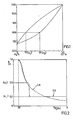
- the invention is based on the fact that at a given temperature T within the melting range, there is a difference in composition between Hg 1-x Cd x Te in the liquid state and Hg 1-x Cd x Te in the solid state.
- T melting range
- Fig. 1 there is at equilibrium a liquid phase of composition XL and a solid phase of composition x s , no intermediate composition between XL and x s being able to exist.
- a wafer whose profile is as shown in FIG. 2 is subjected to fusion and which comprises a surface area of composition less than x L , an intermediate area of composition between XL and x s and a composition area greater than x s , the surface area (x ⁇ x L ) changes to the liquid state, the substrate side area (x> x s ) remains in the solid state, and the intermediate area (x L ⁇ x ⁇ x S ) splits into a liquid part and a solid part.
- the cooling freezes this situation and the liquid phase once solidified presents a homogeneous composition x which is the average of the starting compositions in areas that become liquid during fusion.
- the part resulting from the solid phase has a composition at least equal to x s , from which there results an extremely abrupt transition with the surface part.
- the dotted curve 2A shows the composition profile of a thin layer of Hg 1-x Cd x Te deposited by epitaxial growth on a CdTe substrate according to the EDRI technique mentioned above.
- the thickness of the layer is 20 ⁇ m, and the surface composition x is approximately 0.13.
- the EDRI process has been described in detail in numerous publications and there is no need to detail the method of preparation of the starting thin layer.
- the method according to the invention consists in bringing the layer of Hg 1-x Cd x Te to a temperature T within the melting range, and then cooling rapidly.
- the melting temperature T is 800 ° C.
- the compositions XL and x s are defined by the phase diagram of FIG. 1 and equal respectively to 0.2 and 0.5. By plotting these values on the profile of FIG. 2, it can be seen that the starting layer is divided into three zones: a surface zone where the composition is less than 0.2; an interior area adjacent to the substrate, where the composition is greater than 0.5; and an intermediate zone where the composition is between 0.2 and 0.5.
- the layer When the layer is brought to the temperature of 800 ° C., it follows from the phase diagram that the surface zone becomes liquid, the interior zone remains solid and the intermediate zone splits into a part which remains solid and a part which becomes liquid .
- the liquid phase is obviously homogeneous and its proportion of cadmium x is the average value of this proportion over the part of the layer which has passed into the liquid state.
- the sudden cooling causes the solidification of the liquid phase, but does not modify the compositions.
- the final profile obtained is illustrated by curve 2B in solid lines.
- the internal zone it is not modified compared to the initial profile.
- Such a profile allows the wafer thus obtained to be used for manufacturing an infrared detector with illumination from the substrate side or rear face.
- the CdTe substrate the large bandwidth of which is large, is transparent to photons having the wavelength considered, namely situated in the range 8 ⁇ 14 ⁇ m, and the transition zone, given its very small thickness, practically does not absorb photons. These are only absorbed in the surface zone, at the level of the pn junction which has been placed in the vicinity of the transition zone. Since the surface area has only a thin thickness of around 10 ⁇ m, this does not pose any problems.
- the value x obtained in the surface area and equal to 0.20 corresponds to the composition x L which results from the phase diagram. But this coincidence is by no means a necessity, and it appears on the contrary from what precedes that the value x obtained can be different from x L '
- the temperature T determines the thickness e L of the part of the layer which becomes liquid during the fusion, and the value x is the average of f (e) over the thickness e L , i.e. corresponds to the integral
- the example illustrated in Figure 3 relates to a thicker layer.
- the dotted curve 3A gives the initial profile of a layer obtained by the EDRI technique and 175 ⁇ m thick.
- the surface composition Xo of this layer is approximately 0.03.
- Curve 3B in solid lines gives the profile obtained with the treatment according to the invention at 800 ° C.
- FIG. 3 also shows a curve 3C in phantom which illustrates the profile obtained by subjecting the starting layer to an annealing treatment as described in French patent application FR-A-2460545.
- a curve 3C in phantom which illustrates the profile obtained by subjecting the starting layer to an annealing treatment as described in French patent application FR-A-2460545.
- the composition varies from 0.05 to approximately 140 ⁇ m in thickness from the surface.
- the composition increases much more gradually than in the layer obtained according to the invention.
- An infrared detector made from this wafer could therefore not function while being lit on the substrate side.
- FIG. 4 Figures 4, 5 and 6 illustrate the practical implementation of the heat treatment according to the invention.
- the treatment is carried out in an electric oven 10 (cf. FIG. 4).
- a heating element 11 surrounds an enclosure 12 inside which a quartz tube 15 containing the wafers to be treated is suspended.
- the enclosure 12 is tubular and closed at its two ends by pads 13 of refractory material such as quartz wool.
- the tube 15 is placed in the center of the tube 12, therefore in an area where the temperature is constant.
- FIG. 5 shows in section and on a larger scale the bottom of the tube 15.
- the plates to be treated P are stacked inside the tube being separated by annular wedges 16, and discs 17, all these elements also being in quartz.
- FIG. 6 shows the evolution of the temperature T as a function of the time t during the treatment, the treatment temperature being chosen to be equal to 800 ° C.
- the temperature rise phase lasts about 2 h 30 min, this time being linked only to the operation of the oven.
- the actual treatment consists in maintaining the temperature at 800 ° C for a period of approximately 2 h 30 min. At the start of this phase, the temperature is actually very slightly below 800 ° C and the value of 800 ° C is not reached until the end of the treatment. Then we stop the oven and the temperature drops very quickly. The composition profile is thus frozen in its state at the end of the melting phase.
- the treatment according to the invention is therefore very rapid since its overall duration is a little more than 5 hours.
Landscapes
- Engineering & Computer Science (AREA)
- Chemical & Material Sciences (AREA)
- Materials Engineering (AREA)
- Crystallography & Structural Chemistry (AREA)
- Manufacturing & Machinery (AREA)
- Computer Hardware Design (AREA)
- Microelectronics & Electronic Packaging (AREA)
- Power Engineering (AREA)
- Physics & Mathematics (AREA)
- General Physics & Mathematics (AREA)
- Condensed Matter Physics & Semiconductors (AREA)
- Metallurgy (AREA)
- Organic Chemistry (AREA)
- Inorganic Chemistry (AREA)
- Crystals, And After-Treatments Of Crystals (AREA)
- Liquid Deposition Of Substances Of Which Semiconductor Devices Are Composed (AREA)
Applications Claiming Priority (2)
| Application Number | Priority Date | Filing Date | Title |
|---|---|---|---|
| FR8004015 | 1980-02-22 | ||
| FR8004015A FR2484469A1 (fr) | 1980-02-22 | 1980-02-22 | Procede de preparation de couches homogenes de hg1-xcdxte |
Publications (2)
| Publication Number | Publication Date |
|---|---|
| EP0034982A1 EP0034982A1 (fr) | 1981-09-02 |
| EP0034982B1 true EP0034982B1 (fr) | 1984-02-15 |
Family
ID=9238896
Family Applications (1)
| Application Number | Title | Priority Date | Filing Date |
|---|---|---|---|
| EP81400250A Expired EP0034982B1 (fr) | 1980-02-22 | 1981-02-18 | Procédé de préparation de couches homogènes de Hg1-xCdxTe |
Country Status (5)
| Country | Link |
|---|---|
| US (1) | US4435224A (enExample) |
| EP (1) | EP0034982B1 (enExample) |
| JP (1) | JPS6021960B2 (enExample) |
| DE (1) | DE3162193D1 (enExample) |
| FR (1) | FR2484469A1 (enExample) |
Families Citing this family (18)
| Publication number | Priority date | Publication date | Assignee | Title |
|---|---|---|---|---|
| GB2116363B (en) * | 1982-03-03 | 1985-10-16 | Philips Electronic Associated | Multi-level infra-red detectors and their manufacture |
| FR2544131B1 (fr) * | 1983-04-08 | 1985-07-05 | Telecommunications Sa | Detecteur photovoltaique en immersion optique |
| GB8324531D0 (en) * | 1983-09-13 | 1983-10-12 | Secr Defence | Cadmium mercury telluride |
| US4504334A (en) * | 1983-12-23 | 1985-03-12 | Texas Instruments Incorporated | Gettering method for mercury cadmium telluride |
| US4507160A (en) * | 1983-12-23 | 1985-03-26 | Texas Instruments Incorporated | Impurity reduction technique for mercury cadmium telluride |
| FR2557730B1 (fr) * | 1983-12-29 | 1987-01-16 | Menn Roger | Couche photoresistante a variation de composition atomique et son procede de fabrication, cellule photoresistante munie d'une telle couche et d'un filtre de longueur d'onde et arrangement de telles cellules |
| US4589192A (en) * | 1984-11-02 | 1986-05-20 | The United States Of America As Represented By The Secretary Of The Army | Hybrid epitaxial growth process |
| US4588446A (en) * | 1985-02-21 | 1986-05-13 | Texas Instruments Incorporated | Method for producing graded band gap mercury cadmium telluride |
| US4743310A (en) * | 1985-08-26 | 1988-05-10 | Ford Aerospace & Communications Corporation | HGCDTE epitaxially grown on crystalline support |
| US5079610A (en) * | 1985-12-05 | 1992-01-07 | Santa Barbara Research Center | Structure and method of fabricating a trapping-mode |
| US5004698A (en) * | 1985-12-05 | 1991-04-02 | Santa Barbara Research Center | Method of making photodetector with P layer covered by N layer |
| US5182217A (en) * | 1985-12-05 | 1993-01-26 | Santa Barbara Research Center | Method of fabricating a trapping-mode |
| US4914495A (en) * | 1985-12-05 | 1990-04-03 | Santa Barbara Research Center | Photodetector with player covered by N layer |
| FR2593196B1 (fr) * | 1986-01-21 | 1988-04-15 | Telecommunications Sa | Procede de preparation d'un lingot cristallin de hg1-xo cdxo te |
| US4740386A (en) * | 1987-03-30 | 1988-04-26 | Rockwell International Corporation | Method for depositing a ternary compound having a compositional profile |
| US4933207A (en) * | 1988-01-22 | 1990-06-12 | Hughes Aircraft Company | Laser and thermal assisted chemical vapor deposition of mercury containing compounds |
| JP2754765B2 (ja) * | 1989-07-19 | 1998-05-20 | 富士通株式会社 | 化合物半導体結晶の製造方法 |
| US5510644A (en) * | 1992-03-23 | 1996-04-23 | Martin Marietta Corporation | CDTE x-ray detector for use at room temperature |
Family Cites Families (7)
| Publication number | Priority date | Publication date | Assignee | Title |
|---|---|---|---|---|
| US3496024A (en) | 1961-10-09 | 1970-02-17 | Monsanto Co | Photovoltaic cell with a graded energy gap |
| DE1295195B (de) | 1961-12-26 | 1969-05-14 | Minnesota Mining & Mfg | Thermoelektrisches Halbleitermaterial |
| FR1447257A (fr) | 1965-05-25 | 1966-07-29 | Centre Nat Rech Scient | Procédé pour effectuer des dépôts de matériaux volatils par croissance cristalline sur des supports solides |
| US3725135A (en) | 1968-10-09 | 1973-04-03 | Honeywell Inc | PROCESS FOR PREPARING EPITAXIAL LAYERS OF Hg{11 {118 {11 Cd{11 Te |
| US3779803A (en) | 1969-11-17 | 1973-12-18 | Ibm | Infrared sensitive semiconductor device and method of manufacture |
| US3622405A (en) * | 1970-06-22 | 1971-11-23 | Honeywell Inc | Method for reducing compositional gradients in{11 {11 {11 {11 {11 {11 {11 {11 {11 {11 |
| US4105477A (en) | 1977-01-06 | 1978-08-08 | Honeywell, Inc. | Doping of (hg,cd)te with a group va element |
-
1980
- 1980-02-22 FR FR8004015A patent/FR2484469A1/fr active Granted
-
1981
- 1981-02-17 US US06/234,753 patent/US4435224A/en not_active Expired - Lifetime
- 1981-02-18 DE DE8181400250T patent/DE3162193D1/de not_active Expired
- 1981-02-18 EP EP81400250A patent/EP0034982B1/fr not_active Expired
- 1981-02-23 JP JP56024388A patent/JPS6021960B2/ja not_active Expired
Also Published As
| Publication number | Publication date |
|---|---|
| FR2484469B1 (enExample) | 1982-07-02 |
| JPS6021960B2 (ja) | 1985-05-30 |
| DE3162193D1 (en) | 1984-03-22 |
| FR2484469A1 (fr) | 1981-12-18 |
| EP0034982A1 (fr) | 1981-09-02 |
| JPS56134600A (en) | 1981-10-21 |
| US4435224A (en) | 1984-03-06 |
Similar Documents
| Publication | Publication Date | Title |
|---|---|---|
| EP0034982B1 (fr) | Procédé de préparation de couches homogènes de Hg1-xCdxTe | |
| EP0067090B1 (fr) | Procédé de dopage de semi-conducteurs | |
| EP2014803B1 (fr) | Dispositif de fabrication d'un bloc de matériau cristallin avec modulation de la conductivité thermique | |
| FR2815953A1 (fr) | Composant micromecanique et procede de fabrication d'un tel composant | |
| EP0801155A1 (fr) | Dispositif et procédé pour la formation de carbure de silicium (SIC) monocristallin sur un germe | |
| EP0199638A1 (fr) | Procédé de fabrication sur un support isolant d'un film de silicium monocristallin orienté et à défauts localisés | |
| FR2604298A1 (fr) | Procede de realisation d'une prise de contact electrique sur un substrat en hgcdte de conductivite p et application a la fabrication d'une diode n/p | |
| EP3563129B1 (fr) | Detecteur de rayonnement electromagnetique et notamment de rayonnement infrarouge et procede pour sa realisation | |
| FR2460545A1 (fr) | Procede de preparation de couches de hg1-xcdxte | |
| FR3058561A1 (fr) | Procede de fabrication d'un element semi-conducteur comprenant un substrat hautement resistif | |
| FR2827707A1 (fr) | Procede de realisation d'un detecteur bolometrique et detecteur realise selon ce procede | |
| EP1692475B1 (fr) | Dispositif de mesure d energie rayonnante ameliore a deux positions | |
| FR2465319A1 (fr) | Cellule photovoltaique | |
| FR2888399A1 (fr) | Substrat, notamment en carbure de silicium, recouvert par une couche mince de nitrure de silicium stoechiometrique, pour la fabrication de composants electroniques, et procede d'obtention d'une telle couche | |
| FR2905706A1 (fr) | Procede d'elimination par recuit des precipites dans un materiau semi conducteur ii vi | |
| FR2486970A1 (fr) | Procede d'application d'un traitement thermique au tellurure de cadmium et de mercure | |
| EP0045258A2 (fr) | Détecteur photovoltaique sensible dans l'infrarouge proche | |
| FR2816755A1 (fr) | Procede de croissance d'un materiau semi-conducteur massif de type ii-vi | |
| FR2948492A1 (fr) | Recristallisation complete de plaquettes semiconductrices | |
| EP2319072A1 (fr) | Procede de preparation d'une couche mince auto-supportee de silicium cristallise | |
| CA1297763C (fr) | Procede de preparation d'un lingot cristallin de | |
| EP0222438B1 (fr) | Creuset pour l'épitaxie en phase liquide de couches semiconductrices de composition contrôlée | |
| Meuleman et al. | Method for the manufacture of a nuclear detector device | |
| FR2544131A1 (fr) | Detecteur photovoltaique en immersion optique | |
| WO2014177809A1 (fr) | Formation d'une couche semi-conductrice i-iii-vi2 par traitement thermique et chalcogenisation d'un precurseur metallique i-iii |
Legal Events
| Date | Code | Title | Description |
|---|---|---|---|
| PUAI | Public reference made under article 153(3) epc to a published international application that has entered the european phase |
Free format text: ORIGINAL CODE: 0009012 |
|
| AK | Designated contracting states |
Designated state(s): DE GB NL |
|
| 17P | Request for examination filed |
Effective date: 19810924 |
|
| GRAA | (expected) grant |
Free format text: ORIGINAL CODE: 0009210 |
|
| AK | Designated contracting states |
Designated state(s): DE GB NL |
|
| REF | Corresponds to: |
Ref document number: 3162193 Country of ref document: DE Date of ref document: 19840322 |
|
| PLBE | No opposition filed within time limit |
Free format text: ORIGINAL CODE: 0009261 |
|
| STAA | Information on the status of an ep patent application or granted ep patent |
Free format text: STATUS: NO OPPOSITION FILED WITHIN TIME LIMIT |
|
| 26N | No opposition filed | ||
| PGFP | Annual fee paid to national office [announced via postgrant information from national office to epo] |
Ref country code: NL Payment date: 19910228 Year of fee payment: 11 |
|
| PG25 | Lapsed in a contracting state [announced via postgrant information from national office to epo] |
Ref country code: NL Effective date: 19910901 |
|
| NLV4 | Nl: lapsed or anulled due to non-payment of the annual fee | ||
| PGFP | Annual fee paid to national office [announced via postgrant information from national office to epo] |
Ref country code: GB Payment date: 19950214 Year of fee payment: 15 |
|
| PGFP | Annual fee paid to national office [announced via postgrant information from national office to epo] |
Ref country code: DE Payment date: 19950223 Year of fee payment: 15 |
|
| PG25 | Lapsed in a contracting state [announced via postgrant information from national office to epo] |
Ref country code: GB Effective date: 19960218 |
|
| GBPC | Gb: european patent ceased through non-payment of renewal fee |
Effective date: 19960218 |
|
| PG25 | Lapsed in a contracting state [announced via postgrant information from national office to epo] |
Ref country code: DE Effective date: 19961101 |