EP0034982A1 - Procédé de préparation de couches homogènes de Hg1-xCdxTe - Google Patents
Procédé de préparation de couches homogènes de Hg1-xCdxTe Download PDFInfo
- Publication number
- EP0034982A1 EP0034982A1 EP81400250A EP81400250A EP0034982A1 EP 0034982 A1 EP0034982 A1 EP 0034982A1 EP 81400250 A EP81400250 A EP 81400250A EP 81400250 A EP81400250 A EP 81400250A EP 0034982 A1 EP0034982 A1 EP 0034982A1
- Authority
- EP
- European Patent Office
- Prior art keywords
- composition
- layer
- substrate
- zone
- temperature
- Prior art date
- Legal status (The legal status is an assumption and is not a legal conclusion. Google has not performed a legal analysis and makes no representation as to the accuracy of the status listed.)
- Granted
Links
- 238000004519 manufacturing process Methods 0.000 title description 3
- 239000000203 mixture Substances 0.000 claims abstract description 43
- 239000000758 substrate Substances 0.000 claims abstract description 28
- 238000000034 method Methods 0.000 claims abstract description 16
- 229910004613 CdTe Inorganic materials 0.000 claims abstract description 13
- 230000004927 fusion Effects 0.000 claims abstract description 4
- 230000005855 radiation Effects 0.000 claims description 4
- 239000010410 layer Substances 0.000 description 24
- 230000007704 transition Effects 0.000 description 11
- 239000007788 liquid Substances 0.000 description 8
- 230000008018 melting Effects 0.000 description 7
- 238000002844 melting Methods 0.000 description 7
- 235000012431 wafers Nutrition 0.000 description 7
- 239000007791 liquid phase Substances 0.000 description 6
- 238000010587 phase diagram Methods 0.000 description 6
- 239000007787 solid Substances 0.000 description 5
- 238000010438 heat treatment Methods 0.000 description 4
- 239000012071 phase Substances 0.000 description 4
- 229910052793 cadmium Inorganic materials 0.000 description 3
- BDOSMKKIYDKNTQ-UHFFFAOYSA-N cadmium atom Chemical compound [Cd] BDOSMKKIYDKNTQ-UHFFFAOYSA-N 0.000 description 3
- 238000001816 cooling Methods 0.000 description 3
- 238000005286 illumination Methods 0.000 description 3
- 239000007790 solid phase Substances 0.000 description 3
- 229910004262 HgTe Inorganic materials 0.000 description 2
- QSHDDOUJBYECFT-UHFFFAOYSA-N mercury Chemical compound [Hg] QSHDDOUJBYECFT-UHFFFAOYSA-N 0.000 description 2
- 229910052753 mercury Inorganic materials 0.000 description 2
- 239000010453 quartz Substances 0.000 description 2
- VYPSYNLAJGMNEJ-UHFFFAOYSA-N silicon dioxide Inorganic materials O=[Si]=O VYPSYNLAJGMNEJ-UHFFFAOYSA-N 0.000 description 2
- 238000007711 solidification Methods 0.000 description 2
- 230000008023 solidification Effects 0.000 description 2
- 230000003595 spectral effect Effects 0.000 description 2
- 239000002344 surface layer Substances 0.000 description 2
- 239000012494 Quartz wool Substances 0.000 description 1
- 238000010521 absorption reaction Methods 0.000 description 1
- 239000000956 alloy Substances 0.000 description 1
- 229910045601 alloy Inorganic materials 0.000 description 1
- 238000000137 annealing Methods 0.000 description 1
- 238000009792 diffusion process Methods 0.000 description 1
- 230000008020 evaporation Effects 0.000 description 1
- 238000001704 evaporation Methods 0.000 description 1
- 238000002360 preparation method Methods 0.000 description 1
- 239000011819 refractory material Substances 0.000 description 1
- 230000035945 sensitivity Effects 0.000 description 1
- 239000011343 solid material Substances 0.000 description 1
Images

Classifications
-
- H—ELECTRICITY
- H01—ELECTRIC ELEMENTS
- H01L—SEMICONDUCTOR DEVICES NOT COVERED BY CLASS H10
- H01L31/00—Semiconductor devices sensitive to infrared radiation, light, electromagnetic radiation of shorter wavelength or corpuscular radiation and specially adapted either for the conversion of the energy of such radiation into electrical energy or for the control of electrical energy by such radiation; Processes or apparatus specially adapted for the manufacture or treatment thereof or of parts thereof; Details thereof
- H01L31/18—Processes or apparatus specially adapted for the manufacture or treatment of these devices or of parts thereof
- H01L31/1828—Processes or apparatus specially adapted for the manufacture or treatment of these devices or of parts thereof the active layers comprising only AIIBVI compounds, e.g. CdS, ZnS, CdTe
- H01L31/1832—Processes or apparatus specially adapted for the manufacture or treatment of these devices or of parts thereof the active layers comprising only AIIBVI compounds, e.g. CdS, ZnS, CdTe comprising ternary compounds, e.g. Hg Cd Te
-
- C—CHEMISTRY; METALLURGY
- C30—CRYSTAL GROWTH
- C30B—SINGLE-CRYSTAL GROWTH; UNIDIRECTIONAL SOLIDIFICATION OF EUTECTIC MATERIAL OR UNIDIRECTIONAL DEMIXING OF EUTECTOID MATERIAL; REFINING BY ZONE-MELTING OF MATERIAL; PRODUCTION OF A HOMOGENEOUS POLYCRYSTALLINE MATERIAL WITH DEFINED STRUCTURE; SINGLE CRYSTALS OR HOMOGENEOUS POLYCRYSTALLINE MATERIAL WITH DEFINED STRUCTURE; AFTER-TREATMENT OF SINGLE CRYSTALS OR A HOMOGENEOUS POLYCRYSTALLINE MATERIAL WITH DEFINED STRUCTURE; APPARATUS THEREFOR
- C30B11/00—Single-crystal growth by normal freezing or freezing under temperature gradient, e.g. Bridgman-Stockbarger method
-
- C—CHEMISTRY; METALLURGY
- C30—CRYSTAL GROWTH
- C30B—SINGLE-CRYSTAL GROWTH; UNIDIRECTIONAL SOLIDIFICATION OF EUTECTIC MATERIAL OR UNIDIRECTIONAL DEMIXING OF EUTECTOID MATERIAL; REFINING BY ZONE-MELTING OF MATERIAL; PRODUCTION OF A HOMOGENEOUS POLYCRYSTALLINE MATERIAL WITH DEFINED STRUCTURE; SINGLE CRYSTALS OR HOMOGENEOUS POLYCRYSTALLINE MATERIAL WITH DEFINED STRUCTURE; AFTER-TREATMENT OF SINGLE CRYSTALS OR A HOMOGENEOUS POLYCRYSTALLINE MATERIAL WITH DEFINED STRUCTURE; APPARATUS THEREFOR
- C30B19/00—Liquid-phase epitaxial-layer growth
-
- C—CHEMISTRY; METALLURGY
- C30—CRYSTAL GROWTH
- C30B—SINGLE-CRYSTAL GROWTH; UNIDIRECTIONAL SOLIDIFICATION OF EUTECTIC MATERIAL OR UNIDIRECTIONAL DEMIXING OF EUTECTOID MATERIAL; REFINING BY ZONE-MELTING OF MATERIAL; PRODUCTION OF A HOMOGENEOUS POLYCRYSTALLINE MATERIAL WITH DEFINED STRUCTURE; SINGLE CRYSTALS OR HOMOGENEOUS POLYCRYSTALLINE MATERIAL WITH DEFINED STRUCTURE; AFTER-TREATMENT OF SINGLE CRYSTALS OR A HOMOGENEOUS POLYCRYSTALLINE MATERIAL WITH DEFINED STRUCTURE; APPARATUS THEREFOR
- C30B23/00—Single-crystal growth by condensing evaporated or sublimed materials
- C30B23/02—Epitaxial-layer growth
-
- C—CHEMISTRY; METALLURGY
- C30—CRYSTAL GROWTH
- C30B—SINGLE-CRYSTAL GROWTH; UNIDIRECTIONAL SOLIDIFICATION OF EUTECTIC MATERIAL OR UNIDIRECTIONAL DEMIXING OF EUTECTOID MATERIAL; REFINING BY ZONE-MELTING OF MATERIAL; PRODUCTION OF A HOMOGENEOUS POLYCRYSTALLINE MATERIAL WITH DEFINED STRUCTURE; SINGLE CRYSTALS OR HOMOGENEOUS POLYCRYSTALLINE MATERIAL WITH DEFINED STRUCTURE; AFTER-TREATMENT OF SINGLE CRYSTALS OR A HOMOGENEOUS POLYCRYSTALLINE MATERIAL WITH DEFINED STRUCTURE; APPARATUS THEREFOR
- C30B29/00—Single crystals or homogeneous polycrystalline material with defined structure characterised by the material or by their shape
- C30B29/10—Inorganic compounds or compositions
- C30B29/46—Sulfur-, selenium- or tellurium-containing compounds
- C30B29/48—AIIBVI compounds wherein A is Zn, Cd or Hg, and B is S, Se or Te
-
- C—CHEMISTRY; METALLURGY
- C30—CRYSTAL GROWTH
- C30B—SINGLE-CRYSTAL GROWTH; UNIDIRECTIONAL SOLIDIFICATION OF EUTECTIC MATERIAL OR UNIDIRECTIONAL DEMIXING OF EUTECTOID MATERIAL; REFINING BY ZONE-MELTING OF MATERIAL; PRODUCTION OF A HOMOGENEOUS POLYCRYSTALLINE MATERIAL WITH DEFINED STRUCTURE; SINGLE CRYSTALS OR HOMOGENEOUS POLYCRYSTALLINE MATERIAL WITH DEFINED STRUCTURE; AFTER-TREATMENT OF SINGLE CRYSTALS OR A HOMOGENEOUS POLYCRYSTALLINE MATERIAL WITH DEFINED STRUCTURE; APPARATUS THEREFOR
- C30B29/00—Single crystals or homogeneous polycrystalline material with defined structure characterised by the material or by their shape
- C30B29/60—Single crystals or homogeneous polycrystalline material with defined structure characterised by the material or by their shape characterised by shape
-
- H—ELECTRICITY
- H01—ELECTRIC ELEMENTS
- H01L—SEMICONDUCTOR DEVICES NOT COVERED BY CLASS H10
- H01L21/00—Processes or apparatus adapted for the manufacture or treatment of semiconductor or solid state devices or of parts thereof
- H01L21/02—Manufacture or treatment of semiconductor devices or of parts thereof
- H01L21/02104—Forming layers
- H01L21/02365—Forming inorganic semiconducting materials on a substrate
- H01L21/02367—Substrates
- H01L21/0237—Materials
- H01L21/024—Group 12/16 materials
- H01L21/02411—Tellurides
-
- H—ELECTRICITY
- H01—ELECTRIC ELEMENTS
- H01L—SEMICONDUCTOR DEVICES NOT COVERED BY CLASS H10
- H01L21/00—Processes or apparatus adapted for the manufacture or treatment of semiconductor or solid state devices or of parts thereof
- H01L21/02—Manufacture or treatment of semiconductor devices or of parts thereof
- H01L21/02104—Forming layers
- H01L21/02365—Forming inorganic semiconducting materials on a substrate
- H01L21/02436—Intermediate layers between substrates and deposited layers
- H01L21/02439—Materials
- H01L21/02469—Group 12/16 materials
- H01L21/0248—Tellurides
-
- H—ELECTRICITY
- H01—ELECTRIC ELEMENTS
- H01L—SEMICONDUCTOR DEVICES NOT COVERED BY CLASS H10
- H01L21/00—Processes or apparatus adapted for the manufacture or treatment of semiconductor or solid state devices or of parts thereof
- H01L21/02—Manufacture or treatment of semiconductor devices or of parts thereof
- H01L21/02104—Forming layers
- H01L21/02365—Forming inorganic semiconducting materials on a substrate
- H01L21/02436—Intermediate layers between substrates and deposited layers
- H01L21/02494—Structure
- H01L21/02496—Layer structure
- H01L21/0251—Graded layers
-
- H—ELECTRICITY
- H01—ELECTRIC ELEMENTS
- H01L—SEMICONDUCTOR DEVICES NOT COVERED BY CLASS H10
- H01L21/00—Processes or apparatus adapted for the manufacture or treatment of semiconductor or solid state devices or of parts thereof
- H01L21/02—Manufacture or treatment of semiconductor devices or of parts thereof
- H01L21/02104—Forming layers
- H01L21/02365—Forming inorganic semiconducting materials on a substrate
- H01L21/02518—Deposited layers
- H01L21/02521—Materials
- H01L21/02551—Group 12/16 materials
- H01L21/02562—Tellurides
-
- H—ELECTRICITY
- H01—ELECTRIC ELEMENTS
- H01L—SEMICONDUCTOR DEVICES NOT COVERED BY CLASS H10
- H01L21/00—Processes or apparatus adapted for the manufacture or treatment of semiconductor or solid state devices or of parts thereof
- H01L21/02—Manufacture or treatment of semiconductor devices or of parts thereof
- H01L21/02104—Forming layers
- H01L21/02365—Forming inorganic semiconducting materials on a substrate
- H01L21/02656—Special treatments
- H01L21/02664—Aftertreatments
- H01L21/02667—Crystallisation or recrystallisation of non-monocrystalline semiconductor materials, e.g. regrowth
-
- H—ELECTRICITY
- H01—ELECTRIC ELEMENTS
- H01L—SEMICONDUCTOR DEVICES NOT COVERED BY CLASS H10
- H01L29/00—Semiconductor devices specially adapted for rectifying, amplifying, oscillating or switching and having potential barriers; Capacitors or resistors having potential barriers, e.g. a PN-junction depletion layer or carrier concentration layer; Details of semiconductor bodies or of electrodes thereof ; Multistep manufacturing processes therefor
- H01L29/02—Semiconductor bodies ; Multistep manufacturing processes therefor
- H01L29/12—Semiconductor bodies ; Multistep manufacturing processes therefor characterised by the materials of which they are formed
- H01L29/22—Semiconductor bodies ; Multistep manufacturing processes therefor characterised by the materials of which they are formed including, apart from doping materials or other impurities, only AIIBVI compounds
- H01L29/221—Semiconductor bodies ; Multistep manufacturing processes therefor characterised by the materials of which they are formed including, apart from doping materials or other impurities, only AIIBVI compounds including two or more compounds, e.g. alloys
-
- H—ELECTRICITY
- H01—ELECTRIC ELEMENTS
- H01L—SEMICONDUCTOR DEVICES NOT COVERED BY CLASS H10
- H01L31/00—Semiconductor devices sensitive to infrared radiation, light, electromagnetic radiation of shorter wavelength or corpuscular radiation and specially adapted either for the conversion of the energy of such radiation into electrical energy or for the control of electrical energy by such radiation; Processes or apparatus specially adapted for the manufacture or treatment thereof or of parts thereof; Details thereof
- H01L31/0248—Semiconductor devices sensitive to infrared radiation, light, electromagnetic radiation of shorter wavelength or corpuscular radiation and specially adapted either for the conversion of the energy of such radiation into electrical energy or for the control of electrical energy by such radiation; Processes or apparatus specially adapted for the manufacture or treatment thereof or of parts thereof; Details thereof characterised by their semiconductor bodies
- H01L31/0256—Semiconductor devices sensitive to infrared radiation, light, electromagnetic radiation of shorter wavelength or corpuscular radiation and specially adapted either for the conversion of the energy of such radiation into electrical energy or for the control of electrical energy by such radiation; Processes or apparatus specially adapted for the manufacture or treatment thereof or of parts thereof; Details thereof characterised by their semiconductor bodies characterised by the material
- H01L31/0264—Inorganic materials
- H01L31/0296—Inorganic materials including, apart from doping material or other impurities, only AIIBVI compounds, e.g. CdS, ZnS, HgCdTe
- H01L31/02966—Inorganic materials including, apart from doping material or other impurities, only AIIBVI compounds, e.g. CdS, ZnS, HgCdTe including ternary compounds, e.g. HgCdTe
Definitions
- the present invention relates to a process for preparing layers of composition Hg 1-x Cd x Te produced on CdTe substrate, making it possible to obtain a layer of Hg 1-x Cd x Te of very high internal homogeneity and an abrupt transition. with the CdTe substrate.
- Eg 1 , 6 eV for CdTe at 77 ° K.
- the bandwidth is approximately 0.1 eV at 77 ° K and the corresponding spectral sensitivity range is between 8 and 14 ⁇ m.
- x referred to here defines the composition at the surface opposite to the substrate, the proportion of cadmium increasing from x to 1 as one moves away from the external surface.
- the epitaxial layers of Hg1 Cd Te are obtained in an appropriate manner by the EDRI technique (Evaporation Diffusion in Isothermal Regime) described in French patent 1 447 257.
- This process consists in placing a plate of CdTe and a plate of HgTe face to face. inside a vacuum chamber and bring the temperature to a high value constant, generally between 500 and 600 ° C.
- This process gives, in the case of thin layers, a surface composition x insufficient for the needs because at most equal to 0.10-0.15.
- the photons whose - the wavelength is in the spectral range envisaged - for example 8 - 14 ⁇ m - would pass through the substrate, the latter having a large forbidden bandwidth, but would be absorbed by the intermediate zone before reaching the surface zone.
- the illumination of the face on the substrate side can only be envisaged if it is possible to very significantly reduce the absorption of photons by the intermediate zone, therefore the thickness of the latter.
- the invention therefore aims to produce thin epitaxial layers of Hg 1-x Cd x Te on a CdTe substrate having excellent internal homogeneity of the surface layer of Hg 1-x Cd x Te and an abrupt transition between the surface layer and the substrate, therefore a very small thickness of the intermediate zone.
- the invention provides for subjecting a wafer formed of a layer of surface composition Hg 1-x Cd Te epitaxially grown on a CdTe substrate, x being less than the desired value x, to a fusion treatment, then quickly cool the wafer.
- the invention is based on the fact that at a given temperature T within the melting range, there is a difference in composition between Hg 1-x Cd x Te in the liquid state and Hg 1-x Cd x Te in the solid state.
- T melting range
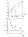
- Fig. 1 there is at equilibrium a liquid phase of composition x L and a solid phase of composition x S , no intermediate composition between x L and x S being able to exist.
- a wafer whose profile is as shown in Figure 2 and which includes a surface area of composition less than x L ; an intermediate zone of composition between x L and x S and a zone of composition greater than x S , the surface zone (x ⁇ x L ) changes to the liquid state, the zone on the substrate side (x> x s ) remains at the solid state, and the intermediate zone (x L ⁇ x ⁇ x S ) splits into a liquid part and a solid part.
- the cooling freezes this situation and the liquid phase once solidified has a homogeneous composition x which is the average of the starting compositions in the zones becoming liquid during the melting.
- the part resulting from the solid phase has a composition at least equal to x S , from which there results an extremely abrupt transition with the surface part.
- the dotted curve 2A shows the composition profile of a thin layer of Hg 1-x Cd x Te deposited by epitaxial growth on a CdTe substrate according to the EDRI technique mentioned above.
- the thickness of the layer is 20 ⁇ m, and the surface composition x is about 0.13.
- the EDRI process has been described in detail in numerous publications and there is no need to detail the method of preparation of the starting thin layer.
- the method according to the invention consists in bringing the layer of Hgl 1-x Cd x Te to a temperature T within the melting range, and then cooling rapidly.
- the compositions x L and x S are defined by the phase diagram of FIG. 1 and equal respectively to 0.2 and 0.5. By plotting these values on the profile of FIG. 2, it can be seen that the starting layer is divided into three zones: a surface zone where the composition is less than 0.2; an interior area adjacent to the substrate, where the composition is greater than 0.5; and an intermediate zone where the composition is between 0.2 and 0.5.
- the layer When the layer is brought to the temperature of 800 ° C., it follows from the phase diagram that the surface zone becomes liquid, the internal zone remains solid and the intermediate zone splits into a part which remains solid and a part which becomes liquid .
- the liquid phase is obviously homogeneous and its proportion of cadmium x is the average value of this proportion over the part of the layer which has passed into the liquid state.
- the sudden cooling causes the solidification of the liquid phase, but does not modify the compositions.
- the final profile obtained is illustrated by curve 2B in solid lines.
- the internal zone it is not modified compared to the initial profile.
- Such a profile allows the wafer thus obtained to be used for manufacturing an infrared detector with illumination from the substrate side or rear face.
- the CdTe substrate the large bandwidth of which is large, is transparent to photons having the wavelength considered, namely located in the range 8 - 14 ⁇ m, and the transition zone, given its very thin thickness, practically does not absorb photons. These are only absorbed in the superficial zone, at the level of the pn junction which has been placed in the vicinity of the transition zone. Since the surface area is only about 10 ⁇ m thick, this poses no problems.
- the value x obtained in the surface area and equal to 0.20 corresponds to the composition x L which results from the phase diagram. But this coincidence is by no means a necessity, and it appears on the contrary from what precedes that the value x obtained can be different from x L.
- the temperature T determines the thickness e L of the part of the layer which becomes liquid during the melting, and the value x is the average of f (e) over the thickness e L , that is to say corresponds to the integral
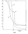
- the example illustrated in Figure 3 relates to a thicker layer.
- the dotted curve 3A gives the initial profile of a layer obtained by the EDRI technique and 175 ⁇ m thick.
- the surface composition x o of this layer is approximately 0.03.
- Curve 3B in solid lines gives the profile obtained with the treatment according to the invention at 800 ° C.
- FIG. 3 also shows a curve 3C in phantom which illustrates the profile obtained by subjecting the starting layer to an annealing treatment as described in French patent application No. 79 17014.
- a weak internal gradient but not negligible in the surface zone since the composition varies from 0.05 to approximately 140 ⁇ m thick from the surface.
- the composition increases much more gradually than in the layer obtained according to the invention. An infrared detector made from this wafer could therefore not function while being lit on the substrate side.
- FIG. 4 Figures 4, 5 and 6 illustrate the practical implementation of the heat treatment according to the invention.
- the treatment is carried out in an electric oven 10 (cf. FIG. 4).
- a heating element 11 surrounds an enclosure 12 inside which a quartz tube 15 containing the wafers to be treated is suspended.
- the enclosure 12 is tubular and closed at its two ends by pads 13 of refractory material such as quartz wool.
- the tube 15 is placed in the center of the tube 12, therefore in an area where the temperature is constant.
- FIG. 5 shows in section and on a larger scale the bottom of the tube 15.
- the plates to be treated P are stacked inside the tube being separated by annular wedges 16, and discs 17, all of these elements also being in quartz.
- FIG. 6 shows the evolution of the temperature T as a function of the time t during the treatment, the treatment temperature being chosen to be equal to 800 ° C.
- the temperature rise phase lasts approximately 2 h 30 min, this time being linked only to the operation of the oven.
- the actual treatment is to maintain the temperature ture at 800 ° C for a period of approximately 2 h 30 min.
- the temperature is actually very slightly below 800 ° C and the value of 800 ° C is not reached until the end of the treatment. Then the oven was stopped and the temperature dropped very quickly.
- the composition profile is thus frozen in its state at the end of the melting phase.
- the treatment according to the invention is therefore very rapid since its overall duration is a little more than 5 hours.
Landscapes
- Engineering & Computer Science (AREA)
- Chemical & Material Sciences (AREA)
- Power Engineering (AREA)
- Microelectronics & Electronic Packaging (AREA)
- Condensed Matter Physics & Semiconductors (AREA)
- Computer Hardware Design (AREA)
- General Physics & Mathematics (AREA)
- Physics & Mathematics (AREA)
- Materials Engineering (AREA)
- Crystallography & Structural Chemistry (AREA)
- Manufacturing & Machinery (AREA)
- Organic Chemistry (AREA)
- Metallurgy (AREA)
- Inorganic Chemistry (AREA)
- Electromagnetism (AREA)
- Ceramic Engineering (AREA)
- Crystals, And After-Treatments Of Crystals (AREA)
- Liquid Deposition Of Substances Of Which Semiconductor Devices Are Composed (AREA)
Abstract
Description
- La présente invention concerne un procédé de préparation de couches de composition Hg1-xCdxTe réalisées sur substrat de CdTe, permettant d'obtenir une couche de Hg1-xCdxTe d'une très grande homogénéité interne et une transition abrupte avec le substrat de CdTe.
- L'alliage Hg1-xCdxTe peut être considéré comme un mélange dans des proportions définies par la valeur de x de HgTe et CdTe, et sa largeur de bande interdite varie en fonction de x à partir d'une valeur Eg = 1,6 eV pour CdTe à 77°K. Pour x = 0,20, la largeur de bande est d'environ 0,1 eV à 77°K et le domaine de sensibilité spectrale correspondant se situe entre 8 et 14 µm.
- Il doit être entendu que la valeur de x dont il est question ici définit la composition à la surface opposée au substrat, la proportion de cadmium augmentant de x jusqu'à 1 à mesure que l'on s'éloigne de la surface extérieure.
- Les couches épitaxiées de Hg1 Cd Te sont obtenues de façon appropriée par la technique EDRI (Evaporation Diffusion en Régime Isotherme) décrite dans le brevet français 1 447 257. Ce procédé consiste à placer face à face une plaquette de CdTe et une plaquette de HgTe à l'intérieur d'une enceinte sous vide et à porter la température à une valeur élevée constante, généralement comprise entre 500 et 600°C. Ce procédé donne, dans le cas de couches minces, une composition superficielle x insuffisante pour les besoins car au plus égale à 0,10-0,15.
- Pour obtenir la valeur de x souhaitée, par exemple x = 0,20, il a été proposé dans le brevet EUA 3 725 135 d'établir dans l'enceinte de traitement une pression de mercure en excès en introduisant dans l'enceinte une certaine quantité de mercure.
- Ce procédé ne procure cependant qu'une homogénéité interne médiocre. En d'autres termes, le gradient Ax/Ae au voisinage de la surface, e étant l'épaisseur de la couche, est trop important. Cela empêche d'utiliser ensuite les techniques applicables aux matériaux massifs.
- De plus, la transition entre la zone superficielle de composition Hg1-xCdx Te et le substrat de CdTe est très progressive, d'où il résulte la présence d'une zone intermédiaire d'épaisseur importante dans laquelle la proportion x de cadmium augmente progressivement jusqu'à la valeur x = 1.
- Ceci présente l'inconvénient qu'il n'est pas possible d'utiliser la face côté substrat en tant que face exposée au rayonnement,car la partie de la zone intermédiaire adjacente à la zone superficielle présente une composition et donc une largeur de bande interdite, voisines de celles de la zone superficielle.
- En cas d'éclairement de la face côté substrat, les photons dont- la longueur d'onde se situe dans le domaine spectral envisagé - par exemple 8 - 14 pm - traverseraient le substrat, celui-ci ayant une largeur de bande interdite importante, mais seraient absorbés par la zone intermédiaire avant d'atteindre la zone superficielle.
- Or il serait intéressant d'éclairer la face côté substrat pour plusieurs raisons. En particulier, comme les connexions électriques nécessaires pour recueillir le courant doivent être placées sur la face opposée au substrat, à proximité de la jonction pn, la face portant les connexions ne serait pas exposée au rayonnement. Cela permettrait de réduire la points surface des jonctions et donc d'augmenter la densité des/ actifs. En outre il deviendrait possible de réaliser le substrat sous forme de lentille concentrant le rayonnement.
- Mais l'éclairement de la face coté substrat n'est envisageable que si l'on parvient à réduire très sensiblement l'absorption des photons par la zone intermédiaire, donc l'épaisseur de celle-ci.
- L'invention vise par conséquent à réaliser des couches minces épitaxiées de Hg1-xCdxTe sur substrat de CdTe présentant une excellente homogénéité interne de la couche superficielle de Hg1-xCdxTe et une transition abrupte entre la couche superficielle et le substrat, donc une très faible épaisseur de la zone intermédiaire.
- Pour atteindre ces buts, l'invention prévoit de soumettre une plaquette formée d'une couche de composition superficielle Hg1-x Cd Te épitaxiée sur un substrat de CdTe, x étant inférieur à Ia valeur souhaitée x, à un traitement de fusion, puis de refroidir rapidement la plaquette.
- L'invention repose sur le fait qu'à une température donnée T comprise dans la plage de fusion, il existe une différence de composition entre le Hg1-xCdxTe à l'état liquide et le Hg1-xCdxTe à l'état solide. Comme cela ressort du diagramme de phases annexé (Fig. 1), on trouve à l'équilibre une phase liquide de composition xL et une phase solide de composition xS, aucune composition intermédiaire entre xL et xS ne pouvant exister.
- Si l'on soumet à la fusion une plaquette dont le profil est tel que représenté à la figure 2 et qui comprend une zone superficielle de composition inférieure à xL; une zone intermédiaire de composition comprise entre xL et xS et une zone de composition supérieure à xS, la zone superficielle (x < xL) passe à l'état liquide, la zone côté substrat (x > xs) reste à l'état solide, et la zone intermédiaire (xL < x < xS) se scinde en une partie liquide et une partie solide. Le refroidissement fige cette situation et la phase liquide une fois solidifiée présente une composition homogène x qui est la moyenne des compositions de départ dans les zones devenant liquides lors de la fusion. On obtient ainsi un gradient Δx/Δe pratiquement nul à partir de la surface dans toute la partie superficielle résultant de la solidification de la phase liquide. Par ailleurs, la partie résultant de la phase solide a une composition au moins égale à xS, d'où il résulte une transition extrêmement abrupte avec la partie superficielle.
- Il est facile de déterminer la température de fusion T pour un profil de composition initial donné de manière à obtenir la valeur x souhaitée, puisqu'à une température T correspondent des valeurs x et xs bien définies.
- L'invention sera bien comprise à la lecture de la description ci-après, faite en référence aux dessins annexés.
- Dans les dessins :
- - la figure 1 montre, comme on l'a dit, le diagramme des phases de Hg1-xCdxTe ;
- - la figure 2 illustre à titre d'exemple le profil de composition obtenu grâce au procédé selon l'invention, dans le cas d'une couche mince ;
- - la figure 3 illustre un autre exemple d'application de l'invention, dans le cas d'une couche plus épaisse ;
- - la figure 4 représente schématiquement un agencement pour la réalisation du traitement thermique;
- - la figure 5 représente, à plus grande échelle, le dispositif supportant les plaquettes; et
- - la figure 6 montre l'évolution de la température lors du traitement thermique selon l'invention.
- La figure 1 est le diagramme de phases de Hg1-xCdxTe qui se compose de la courbe de solidus S et de la courbe de liquidus L. On note qu'à une température donnée, par exemple à 800°C, la phase liquide a une composition xL = 0,2 tandis que la phase solide a une composition xs = 0,5 et qu'il n'existe pas à l'équilibre de composition intermédiaire entre xL et x S.
- Cette propriété est utilisée comme on va le voir pour obtenir des couches de Hg1-xCdxTe épitaxiées sur substrat de CdTe présentant une très grande homogénéité interne et une transition très abrupte avec le substrat.
- Sur la figure 2, la courbe 2A en pointillé montre le profil de composition d'une couche mince de Hg1-xCdxTe déposée par croissance épitaxique sur un substrat de CdTe selon la technique EDRI évoquée plus haut. L'épaisseur de la couche est 20 um, et la composition superficielle x est d'environ 0,13. Le procédé EDRI a été décrit en détail dans de nombreuses publications et il est inutile de détailler le mode de préparation de la couche mince de départ.
- On sait que la technique EDRI donne une bonne homogénéité radiale, mais que l'homogénéité interne n'est pas bonne, en particulier dans le cas d'une couche mince, et on voit sur la courbe 2A que le gradient interne Λx/ Δe,e étantl'épaisseur, est très élevé.
- Le procédé selon l'invention consiste à porter la couche de Hgl 1-xCdxTe à une température T comprise dans la plage de fusion, et à refroidir ensuite rapidement.
- Supposons que la température de fusion T soit 800°C. Les compositions xL et xS sont définies par le diagramme de phases de la figure 1 et égales respectivement à 0,2 et 0,5. En reportant ces valeurs sur le profil de la figure 2, on constate que l'on divise la couche de départ en trois zones : une zone superficielle où la composition est inférieure à 0,2 ; une zone intérieure adjacente au substrat, où la composition est supérieure à 0,5 ; et une zone intermédiaire où la composition est comprise entre 0,2 et 0,5.
- Lorsqu'on porte la couche à la température de 800°C, il résulte du diagramme de phase que la zone superficielle devient liquide, la zone intérieure reste solide et la zone intermédiaire se scinde en une partie qui reste solide et une partie qui devient liquide. La phase liquide est évidemment homogène et sa proportion de cadmium x est la valeur moyenne de cette proportion sur la partie de la couche qui est passée à l'état liquide. Le refroidissement brusque provoque la solidification de la phase liquide, mais ne modifie pas les compositions.
- Le profil final obtenu est illustré par la courbe 2B en trait plein. La zone superficielle de composition x = 0,20 présente un gradient interne nul. Son épaisseur est d'environ 12 µm. A la zone superficielle succède une zone de transition très abrupte, dans laquelle la composition passe de la valeur x = 0,20 à la valeur x = 0,50 sur une épaisseur de l'ordre de 1 à 2 pm. Quant à la zone interne, elle n'est pas modifiée par rapport au profil initial.
- Un tel profil permet d'utiliser la plaquette ainsi obtenue pour fabriquer un détecteur infrarouge à éclairement par la face côté substrat ou face arrière. Le substrat en CdTe, dont la largeur de bande interdite est importante, est transparent aux photons ayant la longueur d'onde considérée, à savoir située dans la plage 8 - 14 pm, et la zone de transition, étant donné sa très faible épaisseur, n'absorbe pratiquement pas les photons. Ceux-ci ne sont absorbés que dans la zone superficielle, au niveau de la jonction pn que l'on a placée au voisinage de la zone de transition. Etant donné que la zone superficielle n'a qu'une épaisseur faible d'environ 10 µm, cela ne pose pas de problèmes.
- Dans l'exemple décrit, la valeur x obtenue dans la zone superficielle et égale à 0,20 correspond à la composition xL qui résulte du diagramme de phases. Mais cette coïncidence n'est nullement une nécessité, et il ressort au contraire de ce qui précède que la valeur x obtenue peut être différente de x L.
- La valeur x dépend en fait du profil initial de la composition xo = f(e) et de la température T à laquelle on effectue la fusion. La température T détermine l'épaisseur eL de la partie de la couche qui devient liquide lors de la fusion, et la valeur x est la moyenne de f(e) sur l'épaisseur eL, c'est-à-dire correspond à l'intégrale

- La courbe 3B en trait plein donne le profil obtenu avec le traitement selon l'invention à 800°C. La zone superficielle homogène ST a une composition x = 0,14 - 0,15 et s'étend sur environ 120 µm. A cette zone superficielle succède une première zone de transition TU très abrupte, d'environ 55 pm d'épaisseur, dans laquelle la composition passe de 0,15 à environ 0,60. Une deuxième zone de transition UV moins abrupte relie la première zone de transition au substrat.
- On a également représenté sur la figure 3 une courbe 3C en trait mixte qui illustre le profil obtenu en soumettant la couche de départ à un traitement de recuit tel que décrit dans la demande de brevet français N° 79 17014. On constate dans ce cas un gradient interne faible, mais non négligeable dans la zone superficielle puisque la composition varie de 0,05 sur environ 140 ïm d'épaisseur à partir de la surface. En outre, dans la zone intermédiaire entre la zone superficielle et le substrat, la composition augmente de façon beaucoup plus progressive que dans la couche obtenue selon l'invention. Un détecteur infrarouge fabriqué à partir de cette plaquette ne pourrait donc fonctionner en étant éclairé du côté substrat.
- Les figures 4, 5 et 6 illustrent la réalisation pratique du traitement thermique selon l'invention. Le traitement est effectué dans un-four électrique 10 (cf. figure 4). Un élément chauffant 11 entoure une enceinte 12 à l'intérieur de laquelle on suspend un tube en quartz 15 contenant les plaquettes à traiter. L'enceinte 12 est tubulaire et fermée à ses deux extrémités par des tampons 13 de matière réfractaire telle que de la laine de quartz. Le tube 15 est placé au centre du tube 12, donc dans une zone où la température est constante.
- La figure 5 montre en coupe et à plus grande échelle le fond du tube 15. Les plaquettes à traiter P sont empilées à l'intérieur du tube en étant séparées par des cales annulaires 16, et des disques 17, tous ces éléments étant également en quartz.
- La figure 6 montre l'évolution de la température T en fonction du temps t au cours du traitement, la température de traitement étant choisie égale à 800°C.
- La phase de montée de la température dure environ 2 h 30 mn, cette durée n'étant liée qu'au fonctionnement du four. Le traitement proprement dit consiste à maintenir la température à 800°C pendant une durée d'environ 2h 30 mn. Au début de cette phase, la température est en fait très légèrement inférieure à 800°C et la valeur de 800°C n'est atteinte que vers la fin du traitement. Ensuite, on arrêté le four et la température tombe très rapidement. Le profil de composition est ainsi figé dans son état à la fin de la phase de fusion.
- Le traitement selon l'invention est donc très rapide puisque sa durée globale est un peu supérieure à 5 heures.
Claims (3)
Applications Claiming Priority (2)
| Application Number | Priority Date | Filing Date | Title |
|---|---|---|---|
| FR8004015 | 1980-02-22 | ||
| FR8004015A FR2484469A1 (fr) | 1980-02-22 | 1980-02-22 | Procede de preparation de couches homogenes de hg1-xcdxte |
Publications (2)
| Publication Number | Publication Date |
|---|---|
| EP0034982A1 true EP0034982A1 (fr) | 1981-09-02 |
| EP0034982B1 EP0034982B1 (fr) | 1984-02-15 |
Family
ID=9238896
Family Applications (1)
| Application Number | Title | Priority Date | Filing Date |
|---|---|---|---|
| EP81400250A Expired EP0034982B1 (fr) | 1980-02-22 | 1981-02-18 | Procédé de préparation de couches homogènes de Hg1-xCdxTe |
Country Status (5)
| Country | Link |
|---|---|
| US (1) | US4435224A (fr) |
| EP (1) | EP0034982B1 (fr) |
| JP (1) | JPS6021960B2 (fr) |
| DE (1) | DE3162193D1 (fr) |
| FR (1) | FR2484469A1 (fr) |
Cited By (2)
| Publication number | Priority date | Publication date | Assignee | Title |
|---|---|---|---|---|
| FR2557730A1 (fr) * | 1983-12-29 | 1985-07-05 | Menn Roger | Couche photoresistante a variation de composition atomique et son procede de fabrication, cellule photoresistante munie d'une telle couche et d'un filtre de longueur d'onde et arrangement de telles cellules |
| US5004698A (en) * | 1985-12-05 | 1991-04-02 | Santa Barbara Research Center | Method of making photodetector with P layer covered by N layer |
Families Citing this family (16)
| Publication number | Priority date | Publication date | Assignee | Title |
|---|---|---|---|---|
| GB2116363B (en) * | 1982-03-03 | 1985-10-16 | Philips Electronic Associated | Multi-level infra-red detectors and their manufacture |
| FR2544131B1 (fr) * | 1983-04-08 | 1985-07-05 | Telecommunications Sa | Detecteur photovoltaique en immersion optique |
| GB8324531D0 (en) * | 1983-09-13 | 1983-10-12 | Secr Defence | Cadmium mercury telluride |
| US4507160A (en) * | 1983-12-23 | 1985-03-26 | Texas Instruments Incorporated | Impurity reduction technique for mercury cadmium telluride |
| US4504334A (en) * | 1983-12-23 | 1985-03-12 | Texas Instruments Incorporated | Gettering method for mercury cadmium telluride |
| US4589192A (en) * | 1984-11-02 | 1986-05-20 | The United States Of America As Represented By The Secretary Of The Army | Hybrid epitaxial growth process |
| US4588446A (en) * | 1985-02-21 | 1986-05-13 | Texas Instruments Incorporated | Method for producing graded band gap mercury cadmium telluride |
| US4743310A (en) * | 1985-08-26 | 1988-05-10 | Ford Aerospace & Communications Corporation | HGCDTE epitaxially grown on crystalline support |
| US5182217A (en) * | 1985-12-05 | 1993-01-26 | Santa Barbara Research Center | Method of fabricating a trapping-mode |
| US5079610A (en) * | 1985-12-05 | 1992-01-07 | Santa Barbara Research Center | Structure and method of fabricating a trapping-mode |
| US4914495A (en) * | 1985-12-05 | 1990-04-03 | Santa Barbara Research Center | Photodetector with player covered by N layer |
| FR2593196B1 (fr) * | 1986-01-21 | 1988-04-15 | Telecommunications Sa | Procede de preparation d'un lingot cristallin de hg1-xo cdxo te |
| US4740386A (en) * | 1987-03-30 | 1988-04-26 | Rockwell International Corporation | Method for depositing a ternary compound having a compositional profile |
| US4933207A (en) * | 1988-01-22 | 1990-06-12 | Hughes Aircraft Company | Laser and thermal assisted chemical vapor deposition of mercury containing compounds |
| JP2754765B2 (ja) * | 1989-07-19 | 1998-05-20 | 富士通株式会社 | 化合物半導体結晶の製造方法 |
| US5510644A (en) * | 1992-03-23 | 1996-04-23 | Martin Marietta Corporation | CDTE x-ray detector for use at room temperature |
Citations (1)
| Publication number | Priority date | Publication date | Assignee | Title |
|---|---|---|---|---|
| US3622405A (en) * | 1970-06-22 | 1971-11-23 | Honeywell Inc | Method for reducing compositional gradients in{11 {11 {11 {11 {11 {11 {11 {11 {11 {11 |
-
1980
- 1980-02-22 FR FR8004015A patent/FR2484469A1/fr active Granted
-
1981
- 1981-02-17 US US06/234,753 patent/US4435224A/en not_active Expired - Lifetime
- 1981-02-18 EP EP81400250A patent/EP0034982B1/fr not_active Expired
- 1981-02-18 DE DE8181400250T patent/DE3162193D1/de not_active Expired
- 1981-02-23 JP JP56024388A patent/JPS6021960B2/ja not_active Expired
Patent Citations (1)
| Publication number | Priority date | Publication date | Assignee | Title |
|---|---|---|---|---|
| US3622405A (en) * | 1970-06-22 | 1971-11-23 | Honeywell Inc | Method for reducing compositional gradients in{11 {11 {11 {11 {11 {11 {11 {11 {11 {11 |
Non-Patent Citations (2)
| Title |
|---|
| Applied Physics Letters, Vol. 34, No. 1, Janvier 1979, US M. LANIR et al.: "Backside-Illuminated HgCdTe/CdTe Photodiodes", pages 50-52 * |
| Journal of the Electrochemical Society, Vol. 125, No. 2, Fevrier 1978, G. FOIRITO et al.: "a Possible Method for the Growth of Homogeneous Mercury Cadmium Telluride Single Crystals", pages 315-317 * |
Cited By (2)
| Publication number | Priority date | Publication date | Assignee | Title |
|---|---|---|---|---|
| FR2557730A1 (fr) * | 1983-12-29 | 1985-07-05 | Menn Roger | Couche photoresistante a variation de composition atomique et son procede de fabrication, cellule photoresistante munie d'une telle couche et d'un filtre de longueur d'onde et arrangement de telles cellules |
| US5004698A (en) * | 1985-12-05 | 1991-04-02 | Santa Barbara Research Center | Method of making photodetector with P layer covered by N layer |
Also Published As
| Publication number | Publication date |
|---|---|
| JPS56134600A (en) | 1981-10-21 |
| DE3162193D1 (en) | 1984-03-22 |
| US4435224A (en) | 1984-03-06 |
| FR2484469B1 (fr) | 1982-07-02 |
| EP0034982B1 (fr) | 1984-02-15 |
| JPS6021960B2 (ja) | 1985-05-30 |
| FR2484469A1 (fr) | 1981-12-18 |
Similar Documents
| Publication | Publication Date | Title |
|---|---|---|
| EP0034982B1 (fr) | Procédé de préparation de couches homogènes de Hg1-xCdxTe | |
| EP0130865B1 (fr) | Dispositif d'élaboration d'un monocristal | |
| FR2918675A1 (fr) | Dispositif de fabrication d'un bloc de materiau cristallin avec modulation de la conductivite thermique. | |
| FR2815953A1 (fr) | Composant micromecanique et procede de fabrication d'un tel composant | |
| EP2894444A1 (fr) | Matériau sensible pour la détection bolométrique | |
| EP0199638A1 (fr) | Procédé de fabrication sur un support isolant d'un film de silicium monocristallin orienté et à défauts localisés | |
| EP3563129B1 (fr) | Detecteur de rayonnement electromagnetique et notamment de rayonnement infrarouge et procede pour sa realisation | |
| FR2827707A1 (fr) | Procede de realisation d'un detecteur bolometrique et detecteur realise selon ce procede | |
| FR2460545A1 (fr) | Procede de preparation de couches de hg1-xcdxte | |
| EP1900012A1 (fr) | Couche de silicium tres sensible a l'oxygene et procede d'obtention de cette couche | |
| EP1692475B1 (fr) | Dispositif de mesure d energie rayonnante ameliore a deux positions | |
| FR2486970A1 (fr) | Procede d'application d'un traitement thermique au tellurure de cadmium et de mercure | |
| FR2816755A1 (fr) | Procede de croissance d'un materiau semi-conducteur massif de type ii-vi | |
| FR2488048A1 (fr) | Detecteur photovoltaique sensible dans l'infrarouge proche | |
| FR2948492A1 (fr) | Recristallisation complete de plaquettes semiconductrices | |
| CA1297763C (fr) | Procede de preparation d'un lingot cristallin de | |
| EP0222438B1 (fr) | Creuset pour l'épitaxie en phase liquide de couches semiconductrices de composition contrôlée | |
| FR3058561A1 (fr) | Procede de fabrication d'un element semi-conducteur comprenant un substrat hautement resistif | |
| FR2544131A1 (fr) | Detecteur photovoltaique en immersion optique | |
| EP1750107B1 (fr) | Détecteur thermique de rayonnements électromagnétiques à éléments d'isolation orientés et dispositif de détection mettant en oeuvre de tels détecteurs | |
| Meuleman | Method for the manufacture of a nuclear detector device | |
| CH720093A2 (fr) | Appareil de frittage ultrarapide à haute température. | |
| WO2024028209A1 (fr) | Détecteur thermique de rayonnement | |
| FR2766614A1 (fr) | Procede de realisation d'une structure par croissance d'un materiau sur un support mis a l'air | |
| FR2557730A1 (fr) | Couche photoresistante a variation de composition atomique et son procede de fabrication, cellule photoresistante munie d'une telle couche et d'un filtre de longueur d'onde et arrangement de telles cellules |
Legal Events
| Date | Code | Title | Description |
|---|---|---|---|
| PUAI | Public reference made under article 153(3) epc to a published international application that has entered the european phase |
Free format text: ORIGINAL CODE: 0009012 |
|
| AK | Designated contracting states |
Designated state(s): DE GB NL |
|
| 17P | Request for examination filed |
Effective date: 19810924 |
|
| GRAA | (expected) grant |
Free format text: ORIGINAL CODE: 0009210 |
|
| AK | Designated contracting states |
Designated state(s): DE GB NL |
|
| REF | Corresponds to: |
Ref document number: 3162193 Country of ref document: DE Date of ref document: 19840322 |
|
| PLBE | No opposition filed within time limit |
Free format text: ORIGINAL CODE: 0009261 |
|
| STAA | Information on the status of an ep patent application or granted ep patent |
Free format text: STATUS: NO OPPOSITION FILED WITHIN TIME LIMIT |
|
| 26N | No opposition filed | ||
| PGFP | Annual fee paid to national office [announced via postgrant information from national office to epo] |
Ref country code: NL Payment date: 19910228 Year of fee payment: 11 |
|
| PG25 | Lapsed in a contracting state [announced via postgrant information from national office to epo] |
Ref country code: NL Effective date: 19910901 |
|
| NLV4 | Nl: lapsed or anulled due to non-payment of the annual fee | ||
| PGFP | Annual fee paid to national office [announced via postgrant information from national office to epo] |
Ref country code: GB Payment date: 19950214 Year of fee payment: 15 |
|
| PGFP | Annual fee paid to national office [announced via postgrant information from national office to epo] |
Ref country code: DE Payment date: 19950223 Year of fee payment: 15 |
|
| PG25 | Lapsed in a contracting state [announced via postgrant information from national office to epo] |
Ref country code: GB Effective date: 19960218 |
|
| GBPC | Gb: european patent ceased through non-payment of renewal fee |
Effective date: 19960218 |
|
| PG25 | Lapsed in a contracting state [announced via postgrant information from national office to epo] |
Ref country code: DE Effective date: 19961101 |