EP0034243A2 - Steckverbindung - Google Patents
Steckverbindung Download PDFInfo
- Publication number
- EP0034243A2 EP0034243A2 EP81100081A EP81100081A EP0034243A2 EP 0034243 A2 EP0034243 A2 EP 0034243A2 EP 81100081 A EP81100081 A EP 81100081A EP 81100081 A EP81100081 A EP 81100081A EP 0034243 A2 EP0034243 A2 EP 0034243A2
- Authority
- EP
- European Patent Office
- Prior art keywords
- plug
- pins
- pin
- connection
- connector
- Prior art date
- Legal status (The legal status is an assumption and is not a legal conclusion. Google has not performed a legal analysis and makes no representation as to the accuracy of the status listed.)
- Granted
Links
Images
Classifications
-
- H—ELECTRICITY
- H01—ELECTRIC ELEMENTS
- H01R—ELECTRICALLY-CONDUCTIVE CONNECTIONS; STRUCTURAL ASSOCIATIONS OF A PLURALITY OF MUTUALLY-INSULATED ELECTRICAL CONNECTING ELEMENTS; COUPLING DEVICES; CURRENT COLLECTORS
- H01R12/00—Structural associations of a plurality of mutually-insulated electrical connecting elements, specially adapted for printed circuits, e.g. printed circuit boards [PCB], flat or ribbon cables, or like generally planar structures, e.g. terminal strips, terminal blocks; Coupling devices specially adapted for printed circuits, flat or ribbon cables, or like generally planar structures; Terminals specially adapted for contact with, or insertion into, printed circuits, flat or ribbon cables, or like generally planar structures
- H01R12/70—Coupling devices
- H01R12/71—Coupling devices for rigid printing circuits or like structures
- H01R12/712—Coupling devices for rigid printing circuits or like structures co-operating with the surface of the printed circuit or with a coupling device exclusively provided on the surface of the printed circuit
- H01R12/716—Coupling device provided on the PCB
-
- H—ELECTRICITY
- H01—ELECTRIC ELEMENTS
- H01R—ELECTRICALLY-CONDUCTIVE CONNECTIONS; STRUCTURAL ASSOCIATIONS OF A PLURALITY OF MUTUALLY-INSULATED ELECTRICAL CONNECTING ELEMENTS; COUPLING DEVICES; CURRENT COLLECTORS
- H01R12/00—Structural associations of a plurality of mutually-insulated electrical connecting elements, specially adapted for printed circuits, e.g. printed circuit boards [PCB], flat or ribbon cables, or like generally planar structures, e.g. terminal strips, terminal blocks; Coupling devices specially adapted for printed circuits, flat or ribbon cables, or like generally planar structures; Terminals specially adapted for contact with, or insertion into, printed circuits, flat or ribbon cables, or like generally planar structures
- H01R12/70—Coupling devices
- H01R12/7076—Coupling devices for connection between PCB and component, e.g. display
Definitions
- the invention relates to a plug connection between electronic components or assemblies provided with plug pins, which are sometimes also referred to as modules, and a circuit card provided with printed circuits or lines.
- Plug connections of this type are generally known. In most constructions of this type which have become known to date, one part of the plug connection contains the plug pins, while the other part has the associated sockets. Plug connections of this type are disclosed, for example, in DE-AS 21 63 340 or in DE-OS 26 04 837.
- an electrical plug connection is worth mentioning in the state of the art, which consists of two identically shaped insulating bodies, each of which contains identical socket parts that are opposed in pairs, wherein in each socket part of each pair there is a plug pin protruding from the insulating body and anchored to it.
- the sockets used here are mostly spring sockets that have to be inserted into the circuit card with a printed circuit and must be soldered to the existing cables. Since such connections must be detachable as plug-in connections, there is always the risk that the spring force of the spring bushes will decrease over time. In addition, spring bushings must always be used with a prescribed orientation. Once the sockets are inserted, the arrangement can be made no longer change. The spring bushes can also be bent during the manufacture of the fully equipped circuit cards and are difficult to straighten again.
- the object of the invention is therefore to provide a novel connector of the type mentioned, which is not only simpler and cheaper to manufacture, but is also easier to monitor for manufacturing errors. Furthermore, the new connector should be easier to adapt to changing conditions.
- the circuit card itself is also provided on its surface at the connecting points with connecting pins and is provided that-a rial consisting of Isoli.ermate- B uchsenplatte, the openings on both surfaces at the connection points corresponding points and the inside has lying electrically conductive sockets, which each serve simultaneously to receive the connector pins and the corresponding connection pins.
- the arrangement is preferably such that the sockets expand up and down from a straight section and that the cross-sectional dimensions of the straight section of each socket correspond approximately to the sum of the cross-sectional dimensions of one plug pin and one connecting pin. It is particularly advantageous in production if the bushings consist of a cylindrical straight section and a section which widens outward in the shape of a funnel at the top and bottom. It is advantageous to manufacture the bushings from a resilient material.
- the longitudinal edges of the material strip forming the sockets are not connected to one another and the inner diameter of the cylindrical section of the sockets is somewhat less than the sum of the diameters of one plug pin and a connector pin.
- the long sides of the material strip forming the bushes overlap in the fully formed bush.
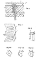
- Fig. 1 shows purely schematically a connector 1 constructed according to the invention between a module, an electrical component or such an assembly 2 with attached plug pins 3 and a circuit card 4 provided with printed circuits or lines.
- the circuit card 4 is with a large number of connection pins 5 provided that are firmly and immovably inserted into the circuit card. In the exemplary embodiment shown here, the connection pins 5 protrude beyond both surfaces of the circuit card 4, although this is not absolutely necessary.
- a socket plate 6 is arranged, which has openings 7 on its top and bottom. To this Openings are followed by a bore 8 in the interior, which serves to receive a socket 9.
- the diameter of the bore 8 is somewhat larger at all points than the diameter of the bushing ..9 shown here of different sizes. The purpose of these diameters of different sizes is explained in more detail.
- the socket plate 6 consists of insulating material, while the socket 9 itself consists of electrically conductive material.
- the arrangement of module 2, socket plate 6 and circuit card 4 is shown purely schematically in FIG. 2.
- a number of connector pins 3 of the module 2, a number of openings 7 in the socket plate 6 and a number of connection pins 5 in the circuit card 4 can again be seen purely schematically.
- One of the sockets 9 is then shown in detail in FIG. 3.
- the socket 9 could have any cross-section and could also have the same cross-section over its entire longitudinal extent, here, in the preferred exemplary embodiment, the socket 9 is designed such that it has a straight section 10 in the middle which goes up and down into an outwardly widening section 11 or 12.
- the straight section 10 is cylindrical and the outwardly widening sections 11 and 12 are funnel-shaped.
- the diameter of the straight section is chosen so that it corresponds approximately to the sum of the cross-sectional dimensions of a connector pin 3 and a connector pin 5.
- the Bushings 9 are made of a resilient material and the diameter of the cylindrical portion of the bushings 9 is slightly less than the sum of the diameters of one plug pin 3 and one connecting pin 5.
- the long sides of the material strip forming the bushes 9 are each other overlap in the fully formed socket. Since the sockets are made of a resilient material and expand in a funnel shape upwards and downwards, the socket is pushed apart somewhat when the plug pins or connecting pins are inserted, thus establishing a secure electrical connection between the plug pin and the connecting pin.
- the cross section of the socket can be, for example, square, hexagonal, circular or else elliptical.
- an elliptical cross section it is possible to use a closed socket. In all other cases, it is more appropriate to use a bushing whose side edges are not connected and which overlap a small distance.
- the socket plate consists of an upper and a lower cover plate 14 or 15 made of insulating material and an intermediate layer 16, which also consists of insulating material.
- the openings 7 in the cover plates 14, 15 are only so large that they each allow the passage of a connector pin or a connector pin.
- Terminal pins are less fragile than the sockets previously used. Faulty connector pins are easier to identify before assembly.
- the insertion of Connection pins can be made faster, since no special alignment as with the sockets previously used is required.
- the distance between the individual connection pins in the circuit card can be changed more easily, since the pins do not have to be punched out at predetermined intervals like the springs. Bent connector pins in a circuit board can easily be bent straight. If a higher density of connection pins is desired, which corresponds to a higher density of the connector pins of the components or assemblies, this can be done more easily with the new plug connection.
- the spring action occurs in a separate part that can be easily removed and replaced:
- the socket plate can also be easily removed if changes have to be made to the circuit card provided with connecting pins or to the module provided with connector pins. It is easy to replace faulty springs after a maximum number of insertion and removal processes.
- the socket plate 6 will first be placed on the circuit card 4 with its connection pins 5 with the aid of a mechanical device. The same device will then be used to drive the components, assemblies or modules with their plug pins into the corresponding sockets of the socket plate. The same device can also be used to disconnect the connector. Overall, you get a connector that is much easier to manufacture and assemble.
Landscapes
- Coupling Device And Connection With Printed Circuit (AREA)
Abstract
Description
- Die Erfindung betrifft eine Steckverbindung zwischen mit Steckerstiften versehenen elektronischen Bauelementen oder Baugruppen, die manchmal auch als Moduln bezeichnet werden, und einer mit gedruckten Schaltungen oder Leitungen versehenen Schaltungskarte.
- Steckverbindungen dieser Art sind allgemein bekannt. Bei den meisten bisher bekannt gewordenen Konstruktionen dieser Art enthält der eine Teil der Steckverbindung die Steckerstifte, während der andere Teil die zugehörigen Buchsen aufweist. Steckverbindungen dieser Art sind beispielsweise in der DE-AS 21 63 340 oder in der DE-OS 26 04 837 offenbart.
- Ferner ist zum Stande der Technik eine elektrische Steckverbindung erwähnenswert, die aus zwei identisch geformten Isolierkörpern besteht, die sich jeweils paarweise gegenüberstehende identische Buchsenteile enthalten, wobei jeweils in einem Buchsenteil jedes Paares ein aus dem Isolierkörper ragender, an diesem verankerter Steckerstift sitzt.
- Derartige Konstruktionen sind relativ teuer und wenig flexibel. Die hier verwendeten Buchsen sind meist Federbuchsen, die in die mit einer gedruckten Schaltung versehene Schaltungskarte eingesetzt und mit den dort vorhandenen Leitungszügen verlötet werden müssen. Da solche Verbindungen als Steckverbindungen lösbar sein müssen, besteht immer die Gefahr, daß mit der Zeit die Federkraft der Federbuchsen nachläßt. Außerdem müssen Federbuchsen stets mit einer vorgeschriebenen Ausrichtung eingesetzt werden. Wenn die Buchsen einmal eingesetzt sind, läßt sich die Anordnung nicht mehr ändern. Ebenfalls können die Federbuchsen bei der Fertigung der vollständig bestückten Schaltungskarten verbogen werden und lassen sich nur schwer wieder richten.
- Aufgabe der Erfindung ist es also, eine neuartige Steckverbindung der eingangs genannten Art zu schaffen, die nicht nur in der Herstellung einfacher und billiger ist, sondern sich auch leichter auf Fertigungsfehler überwachen läßt. Ferner soll sich die neue Steckverbindung auch leichter an geänderte Verhältnisse anpassen lassen. Dies wird erfindungsgemäß dadurch erreicht, daß die Schaltungskarte selbst auf ihrer Oberfläche an den Anschlußpunkten ebenfalls mit Anschlußstiften versehen ist und daß-eine aus Isoli.ermate- rial bestehende Buchsenplatte vorgesehen ist, die auf beiden Oberflächen an den den Anschlußpunkten entsprechenden Stellen öffnungen sowie innen liegende elektrisch leitende Buchsen aufweist, die jeweils gleichzeitig der Aufnahme der Steckerstifte und der entsprechenden Anschlußstifte dienen. Vorzugsweise ist die Anordnung dabei so getroffen, daß die Buchsen sich aus einem geraden Abschnitt nach oben und unten erweitern und daß die Querschnittsabmessungen des geraden Abschnitts jeder Buchse etwa der Summe der Querschnittsabmessungen je eines Steckerstiftes und eines Anschlußstiftes entsprechen. Besonders vorteilhaft in der Herstellung ist es, wenn die Buchsen aus einem zylinderförmigen geraden Abschnitt und je einem sich nach außen trichterförmig sich erweiternden Abschnitt oben und unten bestehen. Dabei ist es vorteilhaft, die Buchsen.aus einem federnden Material herzustellen.
- Von ganz besonderem Vorteil ist es, wenn dabei die Längskanten des die Buchsen bildenden Materialstreifens nicht miteinander verbunden sind und der Innendurchmesser des zylindrischen Abschnitts der Buchsen etwas geringer ist als die Summe der Durchmesser je eines Steckerstiftes und eines Anschlußstiftes. Insbesondere ist es dabei zweckmäßig, wenn sich die Längsseiten des die Buchsen bildenden Materialstreifens in der fertig ausgeformten Buchse überlappen.
- Die Erfindung wird nunmehr anhand eines Ausführungsbeispiels in Verbindung mit den beigefügten Zeichnungen im einzelnen näher erläutert.
- In den Zeichnungen zeigen
- Fig. 1 eine Querschnittsansicht einer Steckverbindung gemäß der Erfindung,
- Fig. 2 schematisch eine Darstellung dieser Steckverbindung,
- Fig. 3 eine perspektivische Ansicht einer Buchse und
- Fign. 4A - 4C
verschiedene Querschnittsansichten einer erfindungsgemäß ausgestalteten Buchse. - Fig. 1 zeigt rein schematisch eine erfindungsgemäß aufgebaute Steckverbindung 1 zwischen einem Modul, einem elektrischen Bauelement oder einer solchen Baugruppe 2 mit daran angebrachten Steckerstiften 3 und einer mit gedruckten Schaltungen oder Leitungen versehenen Schaltungskarte 4. Die Schaltungskarte 4 ist dabei mit einer großen Anzahl von Anschlußstiften 5 versehen, die fest und unverrückbar in die Schaltungskarte eingesetzt sind. Im hier gezeigten Ausführungsbeispiel ragen die Anschlußstifte 5 über beide Oberflächen der Schaltungskarte 4 hinaus, obwohl dies nicht zwingend erforderlich ist. Zwischen dem Modul 2 mit seinem Steckerstift 3 und der Schaltungskarte 4 mit ihrem Anschlußstift 5 ist eine Buchsenplatte 6 angeordnet, die an ihrer Ober- und Unterseite Öffnungen 7 aufweist. An diese öffnungen schließt sich im Innenraum eine Bohrung 8 an, die der Aufnahme einer Buchse 9 dient. Wie man aus Fig. 1 ohne weiteres erkennt, ist der Durchmesser der Bohrung 8 an allen Stellen etwas größer als die hier verschieden groß gezeigten Durchmesser der Buchse ..9. Der Zweck dieser unterschiedlich großen-Durchmesser wird noch näher erläutert.
- Man erkennt ferner, daß die Öffnungen 7 in der Buchsenplatte 6 so groß gewählt sind, daß jeweils nur der Steckerstift 3 von oben oder der Anschlußstift 5 von unten einschiebbar sind. Die Buchsenplatte 6 besteht dabei aus Isoliermaterial, während die Buchse 9-selbst aus elektrisch leitendem Material besteht.
- In Fig. 2 ist rein schematisch die Anordnung von Modul 2, Buchsenplatte 6 und Schaltungskarte 4 gezeigt. Man erkennt wiederum rein schematisch eine Anzahl von Steckerstiften 3 des Moduls 2, eine Anzahl von Öffnungen 7 in der Buchsenplatte 6 und eine Anzahl von Anschlußstiften 5 in der Schaltungskarte 4. In Fig. 3 ist dann eine der Buchsen 9 im einzelnen gezeigt. Obwohl im Prinzip die Buchse 9 jeden beliebigen Querschnitt aufweisen könnte und auch über ihre gesamte Längsausdehnung einen gleich großen Querschnitt besitzen könnte, ist doch hier, in dem bevorzugten Ausführungsbeispiel die Buchse 9 so ausgestaltet, daß sie in der Mitte einen geraden Abschnitt 10 aufweist, der nach oben und nach unten in einen sich nach außen erweiternden Abschnitt 11 bzw. 12 übergeht. In dieser besonderen Ausführungsform der Erfindung ist der gerade Abschnitt 10 zylinderförmig, und die sich nach außen erweiternden Abschnitte 11 und 12 sind trichterförmig ausgestaltet.
- Der Durchmesser des geraden Abschnitts wird dabei so gewählt, daß er etwa der Summe der Querschnittsabmessungen je eines Steckerstiftes 3 und eines Anschlußstiftes 5 entspricht. Es ist jedoch besonders vorteilhaft, wenn die Buchsen 9 aus einem federnden Material bestehen und der Durchmesser des zylindrischen Abschnitts der Buchsen 9 etwas geringer ist als die Summe der Durchmesser je eines Steckerstiftes 3 und eines Anschlußstiftes 5. Von besonderem Vorteil ist es aber, wenn die Längsseiten des die Buchsen 9 bildenden Materialstreifens sich in der fertig ausgeformten Buchse überlappen. Da die Buchsen aus einem federnden Material bestehen und sich nach oben und unten trichterförmig erweitern, wird die Buchse beim Einfügen der Steckerstifte bzw. Anschlußstifte etwas auseinander gedrückt und stellt damit eine sichere elektrische Verbindung zwischen Steckerstift und Anschlußstift her.
- Wie aus Fig. 4 im einzelnen rein schematisch zu erkennen, kann der Querschnitt der Buchse beispielsweise quadratisch, sechseckig, kreisförmig oder auch elliptisch sein. Im Falle eines elliptischen Querschnittes ist es möglich, eine geschlossene Buchse zu verwenden. In allen anderen Fällen ist es zweckmäßiger, eine Buchse zu verwenden, deren Seitenkanten nicht miteinander verbunden sind und die sich eine kleine Strecke überlappen.
- In dem hier gezeigten Ausführungsbeispiel besteht die Buchsenplatte aus einer oberen und einer unteren Deckplatte 14 bzw. 15 aus Isoliermaterial und einer dazwischen liegenden, ebenfalls aus Isoliermaterial bestehenden Schicht 16. Wie bereits erwähnt, sind die Öffnungen 7 in den Deckplatten 14, 15 jeweils nur so groß, daß sie jeweils den Durchtritt eines Steckerstiftes oder aber eines Anschlußstiftes gestatten.
- Die neue Steckverbindung hat nun folgende Vorteile. Anschlußstifte sind weniger zerbrechlich als die bisher gebräuchlichen Buchsen. Fehlerhafte Anschlußstifte lassen sich vor dem Zusammenbau leichter feststellen. Das Einsetzen von Anschlußstiften kann scheller erfolgen, da keine besondere Ausrichtung wie bei den bisher verwendeten Buchsen erforderlich ist. Der Abstand zwischen den einzelnen Anschlußstiften in der Schaltungskarte kann leichter verändert werden, da doe Stifte nicht wie die Federn mit vorgegebenen Abständen ausgestanzt werden müssen. Verbogene Anschlußstifte in einer Schaltungskarte können leicht geradegebogen werden. Falls eine höhere Dichte von Anschlußstiften gewünscht wird, die einer höheren Dichte der Steckerstifte der Bauelemente oder Baugruppen entspricht, so läßt sich dies mit der neuen Steckverbindung leichter durchführen.
- Die Federwirkung tritt in einem gesonderten Teil auf, das leicht entfernt und ausgewechselt werden kann: Die Buchsenplatte kann ebenfalls leicht abgenommen werden, wenn an der mit Anschlußstiften versehenen Schaltungskarte oder an dem mit Steckerstiften versehenen Modul Änderungen vorgenommen werden müssen. Das Auswechseln fehlerhafter Federn nach einer höchstmöglichen Anzahl von Einsetz- und Entnahmevorgängen ist leicht möglich.
- Für das Einsetzen der Baugruppen, Bauelemente oder Moduln mit ihren Steckerstiften in die Buchsenplatte wird man mit Hilfe einer mechanischen Vorrichtung zunächst die Buchsenplatte 6 auf die Schaltungskarte 4 mit ihren Anschlußstiften 5 aufsetzen. Mit der gleichen Vorrichtung wird man dann die Bauelemente, Baugruppen oder Moduln mit ihren Steckerstiften in die entsprechenden Buchsen der Buchsenplatte eintreiben. Die gleiche Vorrichtung kann auch zum Lösen der Steckverbindung eingesetzt werden. Insgesamt erhält man also eine Steckverbindung, die wesentlich einfacher herzustellen und zusammenzubauen ist.
Claims (6)
dadurch gekennzeichnet,
gekennzeichnet,
daß die Buchsen (9) sich aus einem geraden Abschnitt (10) nach oben und unten erweitern (11, 12) und daß die Querschnittsabmessungen des geraden Abschnitts (10) etwa der Summe der Querschnittsabmessungen je eines Steckerstiftes (3) und eines Anschlußstiftes (5) entsprechen.
dadurch gekennzeichnet,
daß die Buchsen (9) aus einem zylinderförmigen geraden Abschnitt (10) und je einem sich nach außen trichterförmig erweiternden Abschnitt (11, 12) bestehen.
gekennzeichnet,
daß die Längsseiten des die Buchsen (9) bildenden Materialstreifens in der fertig ausgeformten Buchse sich überlappen.
dadurch gekennzeichnet,
Applications Claiming Priority (2)
| Application Number | Priority Date | Filing Date | Title |
|---|---|---|---|
| DE3005634 | 1980-02-15 | ||
| DE19803005634 DE3005634A1 (de) | 1980-02-15 | 1980-02-15 | Steckverbindung |
Publications (3)
| Publication Number | Publication Date |
|---|---|
| EP0034243A2 true EP0034243A2 (de) | 1981-08-26 |
| EP0034243A3 EP0034243A3 (en) | 1981-11-04 |
| EP0034243B1 EP0034243B1 (de) | 1983-05-18 |
Family
ID=6094665
Family Applications (1)
| Application Number | Title | Priority Date | Filing Date |
|---|---|---|---|
| EP81100081A Expired EP0034243B1 (de) | 1980-02-15 | 1981-01-08 | Steckverbindung |
Country Status (2)
| Country | Link |
|---|---|
| EP (1) | EP0034243B1 (de) |
| DE (2) | DE3005634A1 (de) |
Cited By (2)
| Publication number | Priority date | Publication date | Assignee | Title |
|---|---|---|---|---|
| GB2128037A (en) * | 1982-09-30 | 1984-04-18 | Control Data Corp | An assembly for connecting circuit boards |
| US5637925A (en) * | 1988-02-05 | 1997-06-10 | Raychem Ltd | Uses of uniaxially electrically conductive articles |
Families Citing this family (8)
| Publication number | Priority date | Publication date | Assignee | Title |
|---|---|---|---|---|
| US4813881A (en) * | 1986-12-29 | 1989-03-21 | Labinal Components And Systems, Inc. | Variable insertion force contact |
| US4927370A (en) * | 1988-01-27 | 1990-05-22 | Unisys Corporation (Formerly Burroughs Corp) | High density connector |
| US4988305A (en) * | 1988-01-28 | 1991-01-29 | Unisys Corp. | High density connectors |
| US5059128A (en) * | 1988-01-28 | 1991-10-22 | Unisys Corporation | Engager matrix |
| US4968263A (en) * | 1990-03-28 | 1990-11-06 | Molex Incorporated | Multi-pin electrical connector with floating terminal pins |
| US5211567A (en) * | 1991-07-02 | 1993-05-18 | Cray Research, Inc. | Metallized connector block |
| AU661813B3 (en) * | 1994-07-13 | 1995-08-03 | Utilux Pty Limited | Electrical connector |
| DE102014224696A1 (de) * | 2014-12-03 | 2016-06-09 | Zf Friedrichshafen Ag | Schaltungsträgeranordnung und Verfahren zum Herstellen einer Schaltungsträgeranordnung |
Family Cites Families (3)
| Publication number | Priority date | Publication date | Assignee | Title |
|---|---|---|---|---|
| US2066876A (en) * | 1934-07-02 | 1937-01-05 | Rca Corp | Wiring system for electrical apparatus |
| FR1443957A (fr) * | 1965-03-31 | 1966-07-01 | Alcatel Sa | Procédé et dispositif de raccordement de circuits électriques |
| DE7529437U (de) * | 1974-09-23 | 1976-10-14 | Thomas & Betts Corp., Elizabeth, N.J. (V.St.A.) |
-
1980
- 1980-02-15 DE DE19803005634 patent/DE3005634A1/de not_active Withdrawn
-
1981
- 1981-01-08 EP EP81100081A patent/EP0034243B1/de not_active Expired
- 1981-01-08 DE DE8181100081T patent/DE3160277D1/de not_active Expired
Cited By (2)
| Publication number | Priority date | Publication date | Assignee | Title |
|---|---|---|---|---|
| GB2128037A (en) * | 1982-09-30 | 1984-04-18 | Control Data Corp | An assembly for connecting circuit boards |
| US5637925A (en) * | 1988-02-05 | 1997-06-10 | Raychem Ltd | Uses of uniaxially electrically conductive articles |
Also Published As
| Publication number | Publication date |
|---|---|
| DE3160277D1 (en) | 1983-07-07 |
| EP0034243A3 (en) | 1981-11-04 |
| EP0034243B1 (de) | 1983-05-18 |
| DE3005634A1 (de) | 1981-08-20 |
Similar Documents
| Publication | Publication Date | Title |
|---|---|---|
| DE2234960C3 (de) | Elektrischer Stecker | |
| DE3318135C2 (de) | ||
| EP0263244B1 (de) | Vorrichtung zum elektronischen Prüfen von Leiterplatten mit Kontaktpunkten in extrem feinem Raster (1/20 bis 1/10 Zoll) | |
| DE68917694T2 (de) | Schaltungsplattenzusammenbau und Kontaktstift, der darin verwendet wird. | |
| DE2406125C3 (de) | Buchsenkontakt | |
| DE19528410C2 (de) | Elektromagnetisches Schaltschütz | |
| EP0117846A1 (de) | Bauelement für Baumodelle, insbesondere Bauspielzeuge | |
| DE2234961C3 (de) | Verfahren zur Herstellung von Steckern für Schaltplatten | |
| DE2203435A1 (de) | Elektrisches Verbinderelement fuer gedruckte Schaltungen | |
| EP0236260A1 (de) | Bauelement für Baumodelle, insbesondere Bauspielzeuge | |
| DE102018105784A1 (de) | Leiterkartenverbinder | |
| EP0034243B1 (de) | Steckverbindung | |
| DE2232928A1 (de) | Elektrische mehrkomponentenvorrichtung | |
| EP0397057A1 (de) | Anordnung zur mechanischen und elektrischen Verbindung einer Ergänzungsleiterplatte an einer Grundleiterplatte | |
| EP3526858B1 (de) | Kontaktvorrichtung, leiterplattenanschlussvorrichtung, und verfahren zur herstellung dieser kontaktvorrichtung. | |
| DE2827487C2 (de) | ||
| DE4218431A1 (de) | Einrichtung zur Verbindung eines Steckverbinders mit einer Leiterplatte | |
| DE3881493T2 (de) | Steckerbuchse für Stiftegitter. | |
| DE3784023T2 (de) | Elektrischer steckverbinder, der eine kombination individueller adapter und steckerstift-elemente als kontaktglied enthaelt. | |
| DE4203239A1 (de) | Schalterstecker | |
| DE3623993A1 (de) | Elektrische kontaktsteckverbindung | |
| DE69418867T2 (de) | Elektrischer verbinder | |
| DE2128136A1 (de) | Elektrisches Verbindungsstuck | |
| DE3231380C2 (de) | Verfahren zur Herstellung eines elektrischen Anschlusses | |
| DE3150075A1 (de) | Elektronisches lehrgeraet |
Legal Events
| Date | Code | Title | Description |
|---|---|---|---|
| PUAI | Public reference made under article 153(3) epc to a published international application that has entered the european phase |
Free format text: ORIGINAL CODE: 0009012 |
|
| AK | Designated contracting states |
Designated state(s): DE FR GB |
|
| PUAL | Search report despatched |
Free format text: ORIGINAL CODE: 0009013 |
|
| AK | Designated contracting states |
Designated state(s): DE FR GB |
|
| 17P | Request for examination filed |
Effective date: 19811005 |
|
| GRAA | (expected) grant |
Free format text: ORIGINAL CODE: 0009210 |
|
| AK | Designated contracting states |
Designated state(s): DE FR GB |
|
| REF | Corresponds to: |
Ref document number: 3160277 Country of ref document: DE Date of ref document: 19830707 |
|
| ET | Fr: translation filed | ||
| PLBE | No opposition filed within time limit |
Free format text: ORIGINAL CODE: 0009261 |
|
| STAA | Information on the status of an ep patent application or granted ep patent |
Free format text: STATUS: NO OPPOSITION FILED WITHIN TIME LIMIT |
|
| 26N | No opposition filed | ||
| PGFP | Annual fee paid to national office [announced via postgrant information from national office to epo] |
Ref country code: GB Payment date: 19901220 Year of fee payment: 11 |
|
| PGFP | Annual fee paid to national office [announced via postgrant information from national office to epo] |
Ref country code: DE Payment date: 19910131 Year of fee payment: 11 |
|
| PGFP | Annual fee paid to national office [announced via postgrant information from national office to epo] |
Ref country code: FR Payment date: 19911218 Year of fee payment: 12 |
|
| PG25 | Lapsed in a contracting state [announced via postgrant information from national office to epo] |
Ref country code: GB Effective date: 19920108 |
|
| GBPC | Gb: european patent ceased through non-payment of renewal fee | ||
| PG25 | Lapsed in a contracting state [announced via postgrant information from national office to epo] |
Ref country code: DE Effective date: 19921001 |
|
| PG25 | Lapsed in a contracting state [announced via postgrant information from national office to epo] |
Ref country code: FR Effective date: 19930930 |
|
| REG | Reference to a national code |
Ref country code: FR Ref legal event code: ST |