EP0031386A1 - Dispositif de memoire a semi-conducteurs - Google Patents
Dispositif de memoire a semi-conducteurs Download PDFInfo
- Publication number
- EP0031386A1 EP0031386A1 EP80901149A EP80901149A EP0031386A1 EP 0031386 A1 EP0031386 A1 EP 0031386A1 EP 80901149 A EP80901149 A EP 80901149A EP 80901149 A EP80901149 A EP 80901149A EP 0031386 A1 EP0031386 A1 EP 0031386A1
- Authority
- EP
- European Patent Office
- Prior art keywords
- memory cell
- cell array
- decoder
- redundancy
- address
- Prior art date
- Legal status (The legal status is an assumption and is not a legal conclusion. Google has not performed a legal analysis and makes no representation as to the accuracy of the status listed.)
- Granted
Links
Images

Classifications
-
- G—PHYSICS
- G11—INFORMATION STORAGE
- G11C—STATIC STORES
- G11C29/00—Checking stores for correct operation ; Subsequent repair; Testing stores during standby or offline operation
- G11C29/70—Masking faults in memories by using spares or by reconfiguring
- G11C29/78—Masking faults in memories by using spares or by reconfiguring using programmable devices
- G11C29/84—Masking faults in memories by using spares or by reconfiguring using programmable devices with improved access time or stability
- G11C29/844—Masking faults in memories by using spares or by reconfiguring using programmable devices with improved access time or stability by splitting the decoders in stages
Definitions
- the present invention relates to a semiconductor memory device and, more particularly, to a semiconductor memory device including a redundancy memory cell array therein.
- a semiconductor memory devive comprises a large number of memory cells arranged along rows and columns which are orthogonal to each other.
- a density of defects generated in such a semiconductor memory device during manufacturing is relatively independent of the integration density of the device, but is dependent on semiconductor manufacturing technology. Therefore, the higher the integration density of the device is, the greater is the ratio of the number of normal memory cells to that of defective momory cells. This is one of the advantages obtained by increasing the integration density of a semiconductor memory device. However, even if the device includes only one defective memory cell therein, the device cannot operate normally, and therefore the device is abandoned.
- a semiconductor memory device In order to be able to operate a semiconductor memory device despite such a defective memory cell, a semiconductor memory device has been known in which a redundancy memory cell array is incorporated with a main memory cell matrix along rows or columns thereof. In this device, when a defective memory cell is detected, the redundancy memory cell array is used instead of a row memory cell array or a column memory cell array including said memory cell. In a semiconductor memory device including such a redundancy memory cell array therein, the manufacturing yield thereof can be improved.
- One conventional semiconductor memory device including a redundancy memory cell array comprises a connection area for connecting a redundancy memory cell array to one of the row memory cell arrays of a main memory cell matrix.
- Another semiconductor memory device including a redundancy memory cell array therein comprises row address decorders (or column address decorders) each of which has a switching circuit for selecting the redundancy memory cell array (Ref.: IEEE Trans. Electron Devices, vol. ED-26, No.6, pp.853-860, June 1979).
- a row address decoder selects the redundancy memory cell array instead of said row memory cell array when the decoder receives a row address signal indicating said row memory cell array.
- the switching circuit is comprises of a programmable read-only memory (which is a so-called PROM) written by laser light or written electrically.
- PROM programmable read-only memory
- the row address decoders should be comprised of the above-mentioned switching circuits whose number is the same as that of the rows of a main memory cell matrix, which necessitates a complex structure.
- Still another conventional semiconductor memory device including a redundancy memory cell array comprises means for comparing one part of an address information such as a row address information with a row address indicating a row memory cell array including a defective memory cell, said row address being given from external terminals, and a switching means for preventing said row address information from being supplied to row address decoders when receiving a coincidence signal generated from the comparing means (Ref. Japanese Patent Laid-Open No. Sho. 52-61933).
- the coincidence signal also serves as a signal for selecting the redundancy memory cell array.
- said row address is represented by a combination of connections between the external terminals and two kinds of power supply lines.
- the number of above-mentioned external terminals must be equal to the number of row address lines, and therefore, the chip size of the device cannot be reduced.
- the switching means for suppressing the row address information requires switching elements which are also equal in number to the row address lines, so that the device is complex in structure. Further, the row address lines are switched directly by the switching means so that the row address signals appearing in the row address lines may be confused which may cause a malfunction of the row address decoders.
- a semiconductor memory device comprising: a main memory cell matrix; a redundancy memory cell array which is incorporated with said main memory cell matrix; a first decoder means for selecting one memory cell array parallel to said redundancy memory cell array within said main memory cell matrix, in accordance with a first address information; a second decoder means for selecting said redundancy memory cell array, in accordance with said first address information; a switching means for stopping the transmission of a clock for precharging said first decoder means thereto, and; a third decoder means for selecting one memory cell array perpendicular to said redundancy memory cell array, within said main memory cell matrix and said redundancy memory cell array, in accordance with a second address information.
- the first decoder means is not precharged and, accordingly, the first decoder means does not operate even when the first decoder means receives the first address information.
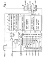
- the device comprises two main memory matrixes 1 and 2 each of which is comprised of 512 memory cells, and sense and refresh amplifier circuit 3 for sensing and refreshing the memory cells arranged between the two main memory cell matrixes 1 and 2.
- the two matrixes 1 and 2 operate as one matrix.
- the device comprises row address buffers 4 and column address buffers 5 for converting a TTL level of address signals A 0 , A 1 , ..., A4 into a MOS level of address signals A 0 , A 1 ..., A 4 and their inverted signals A 0 , A 1 , ..., A 4 , row address decoders 6 for decoding row address signals A 0 , A 0 , A 1 , A 1 , ..., A 4 , A 4 outputted from the row address buffers 4 so as to select one row of the main memory cell matrixes 1 and 2, and column address decoders 7 for decoding column address signals A 0 , A 0 , A 1 , A 1 , ..., A 4 , A 4 outputted from the column address buffers 5 so as to select one column of the main memory cell matrixes 1 and 2.
- such address signals A O , A 1 , ..., A4 of a TTL level are twice supplied to the device for one access thereto.
- a first group of the signals are used for selecting one row of the main memory cell matrixes 1 and 2
- a second group of the signals are used for selecting one column of the main memory cell matrixes 1 and 2.
- Such a time-divisional control of the address signals is effected by three clock generators, i.e., a clock generator 8 which receives an inverted signal of a row address strobe signal RAS and, in turn, generates internal clocks, a clock generator 9 which receives one internal clock of the clock generator 8 and, in turn, generates another internal clock, and a clock generator 10 which receives one internal clock of the clock generator 8 and a column address strobe signal CAS and, in turn, generates another internal clock.
- a clock generator 8 which receives an inverted signal of a row address strobe signal RAS and, in turn, generates internal clocks
- a clock generator 9 which receives one internal clock of the clock generator 8 and, in turn, generates another internal clock
- a clock generator 10 which receives one internal clock of the clock generator 8 and a column address strobe signal CAS and, in turn, generates another internal clock.
- the above-mentioned device comprises a redundancy memory cell array 11 which is incorporated with the main memory cell matrix 1 and corresponds to one row of the main memory- cell matrixes 1 and 2, an additional decoder 12 for selecting the redundancy memory cell array 11, and a switching circuit 13 for stopping the transmission of a clock signal outputted from the clock generator 9 to the row address decoders 6 when receiving a selection signal generated from the decoder 12. Said selection signal is used for selecting the redundancy memory cell array 11.
- the decoder 12 is comprised of a fuse-typed PROM. If a defective memory cell is detected in the main memory cell matrix 1 or 2, a row address to which said defective memory cell belongs is written in the PROM. Of course, when the main memory cell matrixes 1 and 2 include no defective memory cell, the decoder 12 does not execute the selection operation for the redundancy memory cell array 11.
- Reference numeral 14 indicates a data input buffer, for inputting a data DI, which is controlled by a write clock generator 15 which receives a write-enable signal W E .
- reference numeral 16 indicates a data output buffer for outputting a data DO. Both buffers are connected to two data bit lines (not shown) within the sense and refresh amplifiers 3. Further, terminals PI and P 2 are used for writing a defective row address to the decoder 12.
- the decoder 12 and the switching circuit 13 are added to a conventional semiconductor memory device including no redundancy memory cell. Therefore, the parts of said conventional device such as address buffers, address decoders or clock generators are applied to the device according to the present invention, without changing the design thereof.
- all memory cells of the main memory cell matrixes 1 and 2 of a completed semiconductor memory device are tested. After testing, if all of the memory cells of the main memory matrixes 1 and 2 are determined to be normal, the operation of the device is the same as that of a conventional memory device without the redundancy memory cell array 11, the decoder 12 and the switching circuit 13.
- one row array is selected from the main memory cell matrixes 1 and 2 by the row address decoder 6 and, after that, one column array is selected from the main memory cell matrixes 1 and 2 by the column address decoder 7, so that one desired memory cell at an intersecting portion of said one row array and one column is selected.
- a data stored in the desired memory cell is read out to the data output buffer 16, or a new data of the data input buffer 14 is written into the desired memory cell.
- a row address (hereinafter referred to as a defective row address ADD ) to which said row memory cell array is written into the decoder 12 as a fuse-typed PROM by using output signals A 1, A 1, . .., A 4 , A. of the row address buffers 4.
- the decoding operation for the signals A 0 , A 0 , A 1 , A 1 , ... A 4 , A 4 of the row address buffers 4 is effected by either the row address decoders 6 or the decoder 12.
- the decoder 12 does not operate, while the row address decoders 6 operate so as to select one row array among the main memory cell matrixes 1 and 2. After that, the row address decoders 6 operate so as to select one column array of the main memory cell matrixes 1 and 2. As a result, one normal memory cell of the main memory cell matrixes 1 and 2 is selected.
- the decoder 12 operates so as to select the redundancy memory cell array 11 and, accordingly, any of the memory cells of the array 11 can be selected. Simultaneously, the decoder 12 disables the switching circuit 13 so as to stop the transmission of the clock signal of the clock generator 9 to the row address decoders 6.
- the row address decoders 6 cannot be precharged during a stand-by time and, accordingly, the decoders 6 cannot execute selection operation even when the decoders 6 receives the signals A 0 , A 0 , A 1, A 1 , ..., A 4 , A4 from the row address buffers 4. After that, the row address decoders 6 operate so as to select one memory cell of the redundancy memory cell array 11.
- Fig. 2 is a circuit diagram of the decoder 12 for selecting the redundancy memory cell array 11 and the switching circuit 13 of Fig. 1.
- Q 1 is a transistor for precharging a line l 2 connected to the program terminal P when receiving a clock ⁇ 1 .
- Q is a transistor which is connected between the line l 2 via a fuse F and the ground.
- the transistor Q 2 is an element necessary for the operation of the decoder 12, if the fuse F is not melted down.
- a transistor Q 3 connected in parallel to the transistor Q 2 , and transistors Q 4 and Q 5 , for controlling the gate voltage of the transistor Q 3 , which is connected in series between a line l 1 connected to program terminal P 1 and the ground, are elements for writing the decoder 12 as a PROM, in other words, for melting down the fuse F.
- these three transistors Q 3' Q4 and Q 5 are unnecessary for the operation of the decoder 12. Circuit units U 0 , U 0 ', U 1 , ...
- each of which is comprised of the fuse F and the transistors Q 2 , Q 3' Q4 and Q5 are used for receiving the signals A 0 , A 0 , A 1 , ..., A4 outputted from the row address buffers 4, respectively.
- the potential of the line l 2 is applied to the gate of a transistor Q 7 via a transistor Q 6 which serves as a transfer gate, so that the transistor Q 7 is controlled by the potential.
- the switching circuit 13 comprises transistors Q 8 and Q 9 connected in series which together serve as an inverter, and a transistor Q10 controlled by the output of the inverter. For example, if the transistor Q 7 of the decoder 12 is conductive, the transistor Q 9 is also conductive, and the transistor Q 10 is non-conductive.
- the clock signal outputted from the clock generator 9 is supplied to the redundancy memory cell array 11 via the transistor Q 7 , not to the row address decoders 6.
- the transistor Q 7 of the decoder 12 is non-conductive, the transistor Q 9 is also non-conductive, and the transistor Q 10 remains non--conductive.
- the clock signal outputted from the clock generator 9 is supplied to the row address decoders 6, not to the redundancy memory cell array 11.
- the potential of the clock ⁇ 1 (which is in synchronization with the signal RAS and is generated from the clock generator 8 of Fig. 1) is set to be high, so that the transistor Q 4 of the circuit units U 0 , U 0 ' , U 1 , ..., U 4 , is conductive.
- the potential of the line is raised by applying a voltage to the program terminal P 1 , said voltage being high enough that the potentials of nodes N 0 , N 0 , N 1 , ..., N 4 ' is raised.
- the potential of the clock ⁇ 1 is changed from high to low and the signals A 0 , A 0 , A 1 , A4 respresenting a row address ADD x of a defective memory cell array are supplied from the row address buffers 4 to the circuit units U 0 , U0', U 1 , ..., U 4 ', respectively.
- the potentials of the signals A 0 and A 1 are low and the potentials of the signals A 0 and A4 are high, the potentials of the nodes N 0 and N 1 remain high, so that the transistors Q 3 of the circuit units U 0 and U 1 remain conductive, while the potentials of the nodes N 0 ' and N 4 ' are low, so that the transistors Q 3 of the circuit units U 0 ' and U 4 ' are non-conductive.
- the signals A 0 , A 0 , A 1 , ..., A4 are cut off. Even in this state, the transistors Q 3 of the circuit units U 0 and U 1 remain conductive.
- the potential of the line l 2 is raised by applying a voltage to the program terminal P 2 , said voltage being high enough to cause a large current flow from the line l 2 via the fuses F and the transistors Q 3 of the circuit units U 0 and U 1 to the ground and, accordingly, the fuses F of the circuit unit U and U 1 are melted down.
- the fuses F of the circuit units U 0 ' and U 4 ' are not melted down.
- the program terminal P 1 is connected to a V ss terminal (not shown) via a resistor (not shown) of a high resistance, so that, when the potential of the clock ⁇ 1 is high, the transistor Q 3 cannot be conductive. In addition, the program terminal P 2 remains open.
- the decoding operation of the decoder 12 will now be explained.
- the potential of the clock ⁇ 1 is high so that the line l 2 is precharged by a power supply V cc .
- signals A 0 , A 0 , A 1 , ..., A4 are supplied from the row address buffers 4 to the decoder 12. If the signals A 0 , A 0 , A, , ..., A4 correspond to the above-mentioned defective row address ADD , the transistors Q 2 of all the circuit units U 0 , U 0 ', U 1' ... ' U 4 ' remain non-conductive and, accordingly, the potential of the line l 2 remains high and the transistor Q 7 is conductive.
- the clock signal outputted from the clock generator 9 is supplied to the redundancy memory cell array 11 via the transistor Q 7 , not to the row address decoders 6.
- the signals A 0 , A 0 , A 1 , ..., A4 do not correspond to the defective row address ADD at least one transistor Q 2 of the circuit units U 0 , U 0 ', U 1 , ..., U 4 ' is conductive, so that the potential of the line Q2 is low.
- the transistor Q 7 is non-conductive, so that the clock signal generated from the clock generator 9 is supplied to the row address decoders 6, not to the redundancy memory cell array 11.
- one redundancy memory cell array 11 is incorporated with the main memory matrixes 1 or 2 and, accordingly, in spite of a defective memory cell, the device of Fig. 1 can be used (in particular cases, two or more defective memory cells are generated in one row array; the device of Fig. 1 can thus be used in spite of these defects.).
- two or more redundancy memoryy cell arrays 11 can be provided. In this case, the decoders 12 and the switching circuits 13 which are equal in number to the redundancy memory cell arrays are necessary.
- the redundancy memory cell array 11 is incorporated with the main memory cell matrixes 1 and 2 along the rows thereof, but the redundancy memory cell array 11 can also be incorporated with the main memory cell matrixes 1 and 2 along the columns thereof.
- the semiconductor memory device including a redundancy memory cell array therein has the following advantages, as compared with those of the prior art.
Landscapes
- For Increasing The Reliability Of Semiconductor Memories (AREA)
- Techniques For Improving Reliability Of Storages (AREA)
- Static Random-Access Memory (AREA)
Abstract
Applications Claiming Priority (2)
| Application Number | Priority Date | Filing Date | Title |
|---|---|---|---|
| JP7981979A JPS563499A (en) | 1979-06-25 | 1979-06-25 | Semiconductor memory device |
| JP79819/79 | 1979-06-25 |
Publications (3)
| Publication Number | Publication Date |
|---|---|
| EP0031386A1 true EP0031386A1 (fr) | 1981-07-08 |
| EP0031386A4 EP0031386A4 (fr) | 1981-11-25 |
| EP0031386B1 EP0031386B1 (fr) | 1985-09-25 |
Family
ID=13700805
Family Applications (1)
| Application Number | Title | Priority Date | Filing Date |
|---|---|---|---|
| EP80901149A Expired EP0031386B1 (fr) | 1979-06-25 | 1980-06-24 | Dispositif de memoire a semi-conducteurs |
Country Status (5)
| Country | Link |
|---|---|
| US (1) | US4392211A (fr) |
| EP (1) | EP0031386B1 (fr) |
| JP (1) | JPS563499A (fr) |
| DE (1) | DE3071120D1 (fr) |
| WO (1) | WO1981000027A1 (fr) |
Cited By (5)
| Publication number | Priority date | Publication date | Assignee | Title |
|---|---|---|---|---|
| EP0104442A2 (fr) * | 1982-08-30 | 1984-04-04 | Siemens Aktiengesellschaft | Circuit monolitique intégré à semi-conducteur |
| DE3401796A1 (de) * | 1983-01-21 | 1984-07-26 | Hitachi Microcomputer Engineering Ltd., Tokio/Tokyo | Halbleiterspeichervorrichtung |
| EP0274378A2 (fr) * | 1987-01-06 | 1988-07-13 | Kabushiki Kaisha Toshiba | Dispositif de mémoire à semi-conducteur |
| EP0383452A2 (fr) * | 1989-01-31 | 1990-08-22 | Fujitsu Limited | Mémoire à semi-conducteur avec dispositif pour substituer les éléments défectueux |
| EP0499131A1 (fr) * | 1991-02-12 | 1992-08-19 | Texas Instruments Incorporated | Redondance de ligne à haute rendement pour RAM dynamique |
Families Citing this family (23)
| Publication number | Priority date | Publication date | Assignee | Title |
|---|---|---|---|---|
| US4460999A (en) * | 1981-07-15 | 1984-07-17 | Pacific Western Systems, Inc. | Memory tester having memory repair analysis under pattern generator control |
| JPS58164099A (ja) * | 1982-03-25 | 1983-09-28 | Toshiba Corp | 半導体メモリ− |
| JPS58208998A (ja) * | 1982-05-28 | 1983-12-05 | Toshiba Corp | 半導体cmosメモリ |
| US4633429A (en) * | 1982-12-27 | 1986-12-30 | Motorola, Inc. | Partial memory selection using a programmable decoder |
| JPH0666394B2 (ja) * | 1983-12-16 | 1994-08-24 | 富士通株式会社 | 半導体記憶装置 |
| JPS62134899A (ja) * | 1985-12-06 | 1987-06-17 | Mitsubishi Electric Corp | 半導体記憶装置 |
| JPS62153700U (fr) * | 1986-03-20 | 1987-09-29 | ||
| JPS62293598A (ja) * | 1986-06-12 | 1987-12-21 | Toshiba Corp | 半導体記憶装置 |
| JPS6337899A (ja) * | 1986-07-30 | 1988-02-18 | Mitsubishi Electric Corp | 半導体記憶装置 |
| JPH01245497A (ja) * | 1988-03-28 | 1989-09-29 | Nec Corp | 半導体メモリ |
| US5031151A (en) * | 1988-04-01 | 1991-07-09 | International Business Machines Corporation | Wordline drive inhibit circuit implementing worldline redundancy without an access time penalty |
| US5022006A (en) * | 1988-04-01 | 1991-06-04 | International Business Machines Corporation | Semiconductor memory having bit lines with isolation circuits connected between redundant and normal memory cells |
| US5426607A (en) * | 1988-04-27 | 1995-06-20 | Sharp Kabushiki Kaisha | Redundant circuit for memory having redundant block operatively connected to special one of normal blocks |
| WO1990012401A1 (fr) * | 1989-04-13 | 1990-10-18 | Dallas Semiconductor Corporation | Memoire a logique de deconnexion d'alimentation electrique et de redondance |
| KR940008208B1 (ko) * | 1990-12-22 | 1994-09-08 | 삼성전자주식회사 | 반도체 메모리장치의 리던던트 장치 및 방법 |
| US5610631A (en) * | 1992-07-09 | 1997-03-11 | Thrustmaster, Inc. | Reconfigurable joystick controller recalibration |
| US5551701A (en) * | 1992-08-19 | 1996-09-03 | Thrustmaster, Inc. | Reconfigurable video game controller with graphical reconfiguration display |
| US5839517A (en) * | 1993-01-27 | 1998-11-24 | Lord Corporation | Vibration isolator for hand-held vibrating devices |
| JP2710237B2 (ja) * | 1995-09-18 | 1998-02-10 | 日本電気株式会社 | 半導体記憶装置およびその冗長メモリセル部の置換方法 |
| US5732030A (en) * | 1996-06-25 | 1998-03-24 | Texas Instruments Incorporated | Method and system for reduced column redundancy using a dual column select |
| JP2000285694A (ja) * | 1999-03-30 | 2000-10-13 | Mitsubishi Electric Corp | 半導体記憶装置および半導体記憶装置を搭載する半導体集積回路装置 |
| US20030058698A1 (en) * | 2001-09-26 | 2003-03-27 | Gerhard Mueller | Memory with high performance unit architecture |
| US7509543B2 (en) * | 2003-06-17 | 2009-03-24 | Micron Technology, Inc. | Circuit and method for error test, recordation, and repair |
Family Cites Families (4)
| Publication number | Priority date | Publication date | Assignee | Title |
|---|---|---|---|---|
| US3753244A (en) * | 1971-08-18 | 1973-08-14 | Ibm | Yield enhancement redundancy technique |
| US4047163A (en) * | 1975-07-03 | 1977-09-06 | Texas Instruments Incorporated | Fault-tolerant cell addressable array |
| JPS5261933A (en) * | 1975-11-18 | 1977-05-21 | Nec Corp | Memory unit |
| JPS5928560Y2 (ja) * | 1979-11-13 | 1984-08-17 | 富士通株式会社 | 冗長ビットを有する記憶装置 |
-
1979
- 1979-06-25 JP JP7981979A patent/JPS563499A/ja active Granted
-
1980
- 1980-06-24 US US06/243,927 patent/US4392211A/en not_active Expired - Lifetime
- 1980-06-24 DE DE8080901149T patent/DE3071120D1/de not_active Expired
- 1980-06-24 EP EP80901149A patent/EP0031386B1/fr not_active Expired
- 1980-06-24 WO PCT/JP1980/000143 patent/WO1981000027A1/fr active IP Right Grant
Non-Patent Citations (1)
| Title |
|---|
| See references of WO8100027A1 * |
Cited By (10)
| Publication number | Priority date | Publication date | Assignee | Title |
|---|---|---|---|---|
| EP0104442A2 (fr) * | 1982-08-30 | 1984-04-04 | Siemens Aktiengesellschaft | Circuit monolitique intégré à semi-conducteur |
| EP0104442A3 (en) * | 1982-08-30 | 1986-11-26 | Siemens Aktiengesellschaft Berlin Und Munchen | Monolithic integrated semiconductor device |
| DE3401796A1 (de) * | 1983-01-21 | 1984-07-26 | Hitachi Microcomputer Engineering Ltd., Tokio/Tokyo | Halbleiterspeichervorrichtung |
| US4656610A (en) * | 1983-01-21 | 1987-04-07 | Hitachi, Ltd. | Semiconductor memory device having redundancy means |
| EP0274378A2 (fr) * | 1987-01-06 | 1988-07-13 | Kabushiki Kaisha Toshiba | Dispositif de mémoire à semi-conducteur |
| EP0274378A3 (fr) * | 1987-01-06 | 1991-11-27 | Kabushiki Kaisha Toshiba | Dispositif de mémoire à semi-conducteur |
| EP0383452A2 (fr) * | 1989-01-31 | 1990-08-22 | Fujitsu Limited | Mémoire à semi-conducteur avec dispositif pour substituer les éléments défectueux |
| EP0383452A3 (fr) * | 1989-01-31 | 1992-12-23 | Fujitsu Limited | Mémoire à semi-conducteur avec dispositif pour substituer les éléments défectueux |
| EP0686980A1 (fr) * | 1989-01-31 | 1995-12-13 | Fujitsu Limited | Mémoire à semi-conducteur avec dispositif pour substituer les éléments défectueux |
| EP0499131A1 (fr) * | 1991-02-12 | 1992-08-19 | Texas Instruments Incorporated | Redondance de ligne à haute rendement pour RAM dynamique |
Also Published As
| Publication number | Publication date |
|---|---|
| EP0031386B1 (fr) | 1985-09-25 |
| JPS563499A (en) | 1981-01-14 |
| WO1981000027A1 (fr) | 1981-01-08 |
| DE3071120D1 (en) | 1985-10-31 |
| JPS6329360B2 (fr) | 1988-06-13 |
| US4392211A (en) | 1983-07-05 |
| EP0031386A4 (fr) | 1981-11-25 |
Similar Documents
| Publication | Publication Date | Title |
|---|---|---|
| US4392211A (en) | Semiconductor memory device technical field | |
| US4365319A (en) | Semiconductor memory device | |
| US4837747A (en) | Redundary circuit with a spare main decoder responsive to an address of a defective cell in a selected cell block | |
| JP4009686B2 (ja) | 多重メモリ装置モジュールにおける機能をイネーブルにする回路および方法 | |
| KR960013025B1 (ko) | 용장회로의 사용을 외부에서 용이하게 검출할 수 있는 반도체장치 및 반도체 메모리장치 | |
| US4829480A (en) | Column redundancy circuit for CMOS dynamic random access memory | |
| EP0030245B1 (fr) | Dispositif de memoire a semiconducteur | |
| US4648075A (en) | Redundancy circuit for a semiconductor memory device | |
| US5258953A (en) | Semiconductor memory device | |
| US4839864A (en) | Semiconductor memory device comprising programmable redundancy circuit | |
| EP0242981A2 (fr) | Dispositif de mémoire à semi-conducteurs avec partie de circuit à redondance | |
| EP0410413B1 (fr) | Dispositif de mémoire à semiconducteur à réseau de cellules de mémoire de réserve | |
| US4587639A (en) | Static semiconductor memory device incorporating redundancy memory cells | |
| US5555522A (en) | Semiconductor memory having redundant cells | |
| US4752914A (en) | Semiconductor integrated circuit with redundant circuit replacement | |
| US5703816A (en) | Failed memory cell repair circuit of semiconductor memory | |
| EP0102618A2 (fr) | Circuit de mémoire avec des moyens de détection de tension d'alimentation | |
| US5357470A (en) | Semiconductor memory device having redundancy memory cells | |
| KR100309852B1 (ko) | 반도체기억장치 | |
| US4783781A (en) | Semiconductor memory device having redundancy configuration with read circuit for defective memory address | |
| US4987560A (en) | Semiconductor memory device | |
| US6208569B1 (en) | Method of and apparatus for sharing redundancy circuits between memory arrays within a semiconductor memory device | |
| US5390150A (en) | Semiconductor memory device with redundancy structure suppressing power consumption | |
| JPH04255998A (ja) | 半導体記憶装置 | |
| US5612917A (en) | Semiconductor memory device including improved redundancy circuit |
Legal Events
| Date | Code | Title | Description |
|---|---|---|---|
| PUAI | Public reference made under article 153(3) epc to a published international application that has entered the european phase |
Free format text: ORIGINAL CODE: 0009012 |
|
| 17P | Request for examination filed |
Effective date: 19810224 |
|
| AK | Designated contracting states |
Designated state(s): DE FR GB NL |
|
| GRAA | (expected) grant |
Free format text: ORIGINAL CODE: 0009210 |
|
| AK | Designated contracting states |
Designated state(s): DE FR GB NL |
|
| REF | Corresponds to: |
Ref document number: 3071120 Country of ref document: DE Date of ref document: 19851031 |
|
| ET | Fr: translation filed | ||
| PLBE | No opposition filed within time limit |
Free format text: ORIGINAL CODE: 0009261 |
|
| STAA | Information on the status of an ep patent application or granted ep patent |
Free format text: STATUS: NO OPPOSITION FILED WITHIN TIME LIMIT |
|
| 26N | No opposition filed | ||
| PGFP | Annual fee paid to national office [announced via postgrant information from national office to epo] |
Ref country code: FR Payment date: 19990610 Year of fee payment: 20 |
|
| PGFP | Annual fee paid to national office [announced via postgrant information from national office to epo] |
Ref country code: GB Payment date: 19990623 Year of fee payment: 20 |
|
| PGFP | Annual fee paid to national office [announced via postgrant information from national office to epo] |
Ref country code: DE Payment date: 19990626 Year of fee payment: 20 |
|
| PGFP | Annual fee paid to national office [announced via postgrant information from national office to epo] |
Ref country code: NL Payment date: 19990628 Year of fee payment: 20 |
|
| PG25 | Lapsed in a contracting state [announced via postgrant information from national office to epo] |
Ref country code: GB Free format text: LAPSE BECAUSE OF EXPIRATION OF PROTECTION Effective date: 20000623 |
|
| PG25 | Lapsed in a contracting state [announced via postgrant information from national office to epo] |
Ref country code: NL Free format text: LAPSE BECAUSE OF EXPIRATION OF PROTECTION Effective date: 20000624 |
|
| REG | Reference to a national code |
Ref country code: GB Ref legal event code: PE20 Effective date: 20000623 |
|
| NLV7 | Nl: ceased due to reaching the maximum lifetime of a patent |
Effective date: 20000624 |