EP0013598B1 - Dispositif de correction de linéarité et de correction en coussin est-ouest combinées - Google Patents
Dispositif de correction de linéarité et de correction en coussin est-ouest combinées Download PDFInfo
- Publication number
- EP0013598B1 EP0013598B1 EP80300023A EP80300023A EP0013598B1 EP 0013598 B1 EP0013598 B1 EP 0013598B1 EP 80300023 A EP80300023 A EP 80300023A EP 80300023 A EP80300023 A EP 80300023A EP 0013598 B1 EP0013598 B1 EP 0013598B1
- Authority
- EP
- European Patent Office
- Prior art keywords
- winding
- core
- magnetic
- correction
- linearity
- Prior art date
- Legal status (The legal status is an assumption and is not a legal conclusion. Google has not performed a legal analysis and makes no representation as to the accuracy of the status listed.)
- Expired
Links
Images
Classifications
-
- H—ELECTRICITY
- H04—ELECTRIC COMMUNICATION TECHNIQUE
- H04N—PICTORIAL COMMUNICATION, e.g. TELEVISION
- H04N3/00—Scanning details of television systems; Combination thereof with generation of supply voltages
- H04N3/10—Scanning details of television systems; Combination thereof with generation of supply voltages by means not exclusively optical-mechanical
- H04N3/16—Scanning details of television systems; Combination thereof with generation of supply voltages by means not exclusively optical-mechanical by deflecting electron beam in cathode-ray tube, e.g. scanning corrections
- H04N3/22—Circuits for controlling dimensions, shape or centering of picture on screen
- H04N3/23—Distortion correction, e.g. for pincushion distortion correction, S-correction
- H04N3/237—Distortion correction, e.g. for pincushion distortion correction, S-correction using passive elements, e.g. diodes
-
- H—ELECTRICITY
- H01—ELECTRIC ELEMENTS
- H01J—ELECTRIC DISCHARGE TUBES OR DISCHARGE LAMPS
- H01J29/00—Details of cathode-ray tubes or of electron-beam tubes of the types covered by group H01J31/00
- H01J29/46—Arrangements of electrodes and associated parts for generating or controlling the ray or beam, e.g. electron-optical arrangement
- H01J29/70—Arrangements for deflecting ray or beam
Definitions
- This invention relates to combined side pincushion and linearity correction magnetic structures and circuits.
- a linearity coil In typical color television receivers, two separate magnetic components are connected in series with the horizontal deflection winding: a linearity coil, and an East-West or side pincushion correction coil or transformer.
- the linearity coil may be wound on a rod or H-shaped core with one or more bias magnets located adjacent the core.
- the East-West coil may be wound on a separate ferrite rod core or on a closed core like a UU or an EE-shaped core.
- the East-West (E-W) coil may be part of an ITR (Integrated Thyristor Rectifier) controlled E-W modulator circuit such as described in US-A-4,088,931, by P. E. Haferl, or may be part of a diode modulator circuit such as described in US-A-3,906,305, by A. H. H. J. Nillesen.
- East-West correction results in a vertical rate modulation of the horizontal deflection or scanning current.
- the vertical rate modulation of the horizontal scanning current causes an undesirable vertical rate modulation of the magnetic bias of the linearity coil.
- the effect of the linearity coil is thus different at the top or bottom of the raster than in the center, resulting in uncorrected raster distortion.
- the biasing of the linearity coil is sometimes modulated at a vertical rate by coupling the E-W modulator current through an extra winding on the linearity coil, as described, for example, in US-A-4,024,432, by A. Boekhorst.
- Document FR-A-2335096 discloses a structure according to the pre-characterizing part of claim 1 in which the invention is set out, and to which reference should now be made.
- a magnetic structure in accordance with a preferred embodiment of the invention, includes a magnetic core having first and second core portions.
- a first winding is wound around the first core portion and is suited for coupling to a horizontal deflection winding.
- the second winding is wound around the second core portion and is suited for receiving a correction current including a vertical deflection rated complement.
- Magnetic biasing means provides a magnetic bias flux to the first core portion for providing linearity correction to horizontal scanning current flowing in the horizontal deflection winding.
- the first and second core portions are so configured as to establish a high reluctance path for mutual flux linking the first and second windings, for coupling only a portion of the flux generated by the second winding to the first core portion.
- the winding polarities of the first and second windings are such as to enable the portion of the flux generated by the second winding to compensate for undesirable changes during vertical scan of the magnetic bias of the first core portion.
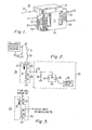
- a combined linearity and side pincushion correction structure 26 embodying the invention and constructed on a single E-shaped magnetic core 21 is illustrated in Figure 1.
- An L-shaped portion 21 a is magnetically biased by a permanent magnet 22, which has magnetic poles located on opposite ends of the surface that is in contact with the core.
- a south pole of magnet 22 is, illustratively, located adjacent a center leg 21 of core 21 and a north pole is located adjacent the outer L-shaped portion 21 a.
- a winding 23, wound around portion 21 a of core 21, is coupled in series with a horizontal deflection winding 50 of a horizontal deflection circuit, as illustrated in the electrical schematic diagram of Figure 2.
- a conductor 12 of winding 23 is coupled to one terminal of horizontal deflection winding 50.
- Another terminal of horizontal deflection winding 50 is coupled at a terminal 61 to a conventional horizontal deflection generator 52 through a trace capacitor 51, for producing horizontal scanning current in deflection winding 50.
- a horizontal retrace capacitor 60 is coupled to terminal
- the magnetic field in the core developed by permanent magnet 22 and by the current flowing in winding 23 is such that at the beginning of horizontal scan the core portion 21 a is near saturation.
- core portion 21 a Toward the center of horizontal scan, core portion 21 a saturates more and more, until, in the second half of horizontal scan, core portion 21 a is substantially in saturation.
- Center leg 21 c because of its larger cross-section is not saturated and thus functions as a magnetic shunt for the entire scan.
- the effect of the inductance variation of portion 21 a is that during the first half of horizontal scan, a decreasing linearity inductance is in series with the deflection winding, while during the second half of scan, because of saturation, little inductance is present.
- This changing inductance during each horizontal scan causes a decreased horizontal deflection current amplitude in the first half of scan which compensates for the non-linearity of the deflection current in the second half of scan caused by the cumulative losses in the deflection winding and the trace switch, for example.
- Winding 23 thereby functions as the required saturable linearity inductance in series with horizontal deflection winding 50.
- a conductor 14 of winding 25 is coupled through a capacitor 53 to a bi-directionally conductive ITR switch 54 of an East-West or side ITR modulator circuit 55.
- Switch 54 may comprise an SCR 56 and an oppositely poled diode 57 integrated on the same chip.
- a resistor 58 is coupled across ITR switch 54.
- a control circuit 59 is coupled to the gate of SCR 56 and turns on SCR 56 at a vertically varying instant with horizontal retrace. The length of time within horizontal retrace that the inductance of winding 25 is coupled to horizontal deflection winding 50 is thereby varied at a vertical rate, thereby modulating the horizontal scanning current amplitude at a vertical rate for providing side pincushion distortion correction.
- Control circuit 59 and East-West ITR modulator 55 are fully described in the aforementioned US-A-4,088,931 of P. E. Haferl.
- a compensating magnetic flux with a compensating vertical rate flux component is made to flow in portion 21a.
- This compensating flux is developed by the current flowing in side pincushion correction inductance winding 25, which has flowing in it the horizontal scanning current during each horizontal trace interval.
- Conductor 14 of side pincushion inductance winding 25 is coupled to a conductor 11 of linearity inductance winding 23, as illustrated in Figures 1 and 2.
- a conductor 13 of winding 25 is coupled to ground.
- horizontal deflection winding 50, linearity inductance winding 23, and side pincushion inductance winding 25 are series connected.
- the vertically modulated horizontal scanning current flows in all three windings. With the winding polarities of windings 23 and 25 as indicated by the polarity dots in Figures 2 and 3, the flux generated by the current flowing in side pincushion inductance winding 25 flows in center leg 21 c in the same direction as the flux generated in leg 21 a by the current flowing in linearity inductance winding 23.
- the horizontal deflection current flowing in linearity winding 23, and thus the flux developed by this current flowing in outer leg 21 a, is smaller at the top and bottom of the raster than in the center.
- the current flowing in side pincushion correction inductance of the East-West ITR modulator circuit 55, and thus the flux flowing in center leg 21 c, developed by this current is larger at the top and bottom of the raster than in the center.
- the increasing flux in center leg 21 compensates for the decreasing flux produced by linearity winding 23.
- the flux produced by winding 25 changes the magnetic bias of portion 21 a in a manner which corrects for the undesirable change in magnetic bias caused by the vertical rate component of the current flowing in linearity inductance winding 23.
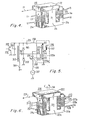
- Figure 3 illustrates that portion of the electrical schematic circuit of Figure 2 associated with another combined linearity and side pincushion structure 126 embodying the invention, similar to the structure 26 of Figure 1.
- Figure 4 illustrates the core, winding and magnet arrangement for structure 126.
- a transformer comprising a tapped winding 125, is substituted for the side pincushion correction winding 25 of Figures 1 and 2.
- a tap conductor 14a instead of the lead conductor 14 of Figures 1 and 2, is now coupled to conductor 11 of linearity inductance winding 23.
- the circuit arrangement of Figure 3 has the advantage that the current through ITR 54 is transformed down which results in lower dissipation in the device. Also a smaller valued capacitor 53 is required.
- Modulator circuits other than East-West ITR modulator circuit 55 of Figure 2 may be coupled to a combined linearity and side pincushion correction structure embodying the invention.
- a diode modulator circuit 255 may be coupled to a combined linearity and side pincushion correction structure 226.
- structure 226 is generally constructed similar to the construction of structures 26 and 126 of Figures 1 and 4.
- An E-shaped core 221 includes a first outer leg or L-shaped portion 221a, a center leg 221 c, and a second outer leg 221 b.
- a linearity inductance winding 223 is wound around outer leg 221a.
- a permanent bias magnet 222, slidable along the line 224, and rotatable about an axis 236, is in contact with legs 221 a and 221 b but is not in close contact with leg 221 b.
- Wound around outer leg 221 b is a winding 225a for correcting side pincushion distortion with a diode modulator.
- Concentrically wound with winding 225a is a transformer coupled secondary winding 225b.
- a conductor 213 of secondary winding 225b is coupled to ground and a conductor 214 is coupled to a conductor 211 of linearity inductance winding 223.
- a conductor 212 of winding 223 is coupled to a horizontal deflection winding 250.
- Horizontal deflection winding 250 is coupled to the collector of a horizontal output transistor 262 of a horizontal deflection generator 252 through a trace capacitor 251.
- the transistor is switched at a horizontal rate by a conventional horizontal oscillator and driver circuit, not illus-. trated.
- the collector of transistor 262 is coupled through a winding of a horizontal output or flyback transformer 263 to a B+ supply voltage developed at a terminal 264.
- a damper diode 265 and retrace capacitor 266 are coupled to transistor 262.
- Diode modulator circuit 255 includes a diode 265', a capacitor 266', a capacitor 251' and a modulation voltage source 267 coupled to capacitor 251' through an inductor 270.
- Modulation voltage source 267 provides a vertical rate parabolic voltage Vm at a terminal 268, with voltage Vm having a minimum at the center of vertical trace.
- a conductor 215 of side pincushion correction inductance winding 225a is coupled to terminal 268 and a conductor 216 is coupled to the junction of diodes 265 and 265'.
- Diode 265', capacitors 266' and 251' of diode modulator circuit 255 function analogously to respective diode 265, and capacitors 266 and 251 associated with horizontal deflection generator 252 for developing a horizontal sawtooth correction current in side pincushion correction inductance winding 225a.
- the values of capacitors 266 and 266' and the location of the tap on flyback transformer winding 263 are selected such that the currents flowing in deflection winding 250 and in winding 225a have the same horizontal retrace time.
- the amplitude of the sawtooth current flowing in winding 225a is modulated in a parabolic vertical manner.
- This modulated sawtooth current is transformed by secondary winding 225b to provide a parabolic vertical rate amplitude modulated sawtooth component to the horizontal scanning current, thereby providing the required side pincushion distortion correction.
- the circuit of Figure 5 is similar in operation to arrangements described in the aforementioned US-A-4,024,432 by A. Boekhorst and US-A-3,906,305 by A. H. H. J. Nillesen.
- one magnetic component 26, 126 or 226 replaces two separate components.
- a conventional linearity coil may use one ferrite rod core and two magnets and a separate E-W modulator structure may use a separate UU, EE or rod- shaped core.
- compensatory modulation of the linearity inductance at a vertical frequency rate is obtained by a single structure which also functions to provide, without additional complexity, or separate support housing, a side pincushion correction inductance.
- Type of kinescope used is A67-700X.
- Magnet 22 may be similar to the magnet used in a N-S pincushion transductor, such as Oréga 5712, manufactured by Orega, France.
Landscapes
- Engineering & Computer Science (AREA)
- Multimedia (AREA)
- Signal Processing (AREA)
- Details Of Television Scanning (AREA)
Claims (4)
Priority Applications (1)
| Application Number | Priority Date | Filing Date | Title |
|---|---|---|---|
| AT80300023T ATE1618T1 (de) | 1979-01-10 | 1980-01-03 | Vorrichtung fuer eine kombinierte linearitaetsund ost-west-kissenkorrektur. |
Applications Claiming Priority (4)
| Application Number | Priority Date | Filing Date | Title |
|---|---|---|---|
| GB7900924 | 1979-01-10 | ||
| GB7900924 | 1979-01-10 | ||
| US32252 | 1979-04-23 | ||
| US06/032,252 US4234824A (en) | 1979-01-10 | 1979-04-23 | Combined linearity and side pincushion correction arrangement |
Publications (2)
| Publication Number | Publication Date |
|---|---|
| EP0013598A1 EP0013598A1 (fr) | 1980-07-23 |
| EP0013598B1 true EP0013598B1 (fr) | 1982-09-29 |
Family
ID=26270183
Family Applications (1)
| Application Number | Title | Priority Date | Filing Date |
|---|---|---|---|
| EP80300023A Expired EP0013598B1 (fr) | 1979-01-10 | 1980-01-03 | Dispositif de correction de linéarité et de correction en coussin est-ouest combinées |
Country Status (8)
| Country | Link |
|---|---|
| EP (1) | EP0013598B1 (fr) |
| AU (1) | AU529782B2 (fr) |
| DD (1) | DD148429A5 (fr) |
| DE (1) | DE3060881D1 (fr) |
| DK (1) | DK10380A (fr) |
| ES (1) | ES487558A1 (fr) |
| FI (1) | FI67982C (fr) |
| NZ (1) | NZ192568A (fr) |
Families Citing this family (5)
| Publication number | Priority date | Publication date | Assignee | Title |
|---|---|---|---|---|
| US2576400A (en) * | 1948-05-08 | 1951-11-27 | Howie Alexander | Scaffolding connection |
| US4516058A (en) * | 1981-05-11 | 1985-05-07 | Rca Corporation | Linearity corrected horizontal deflection circuit |
| NL8500624A (nl) * | 1985-03-06 | 1986-10-01 | Philips Nv | Beeldweergeefinrichting bevattende een lijnsynchroniseerschakeling en een lijnafbuigschakeling. |
| PT84306B (pt) * | 1986-02-27 | 1989-10-04 | Gen Electric | Dispositivo de deflexao |
| US5841023A (en) * | 1993-08-31 | 1998-11-24 | Boehringer Mannheim Corporation | Magnet for medical instrument |
Family Cites Families (1)
| Publication number | Priority date | Publication date | Assignee | Title |
|---|---|---|---|---|
| DE2555300A1 (de) * | 1975-12-09 | 1977-06-23 | Philips Patentverwaltung | Schaltungsanordnung zum erzeugen eines gleichstromes in einer wechselstrom-impedanz |
-
1980
- 1980-01-03 DE DE8080300023T patent/DE3060881D1/de not_active Expired
- 1980-01-03 EP EP80300023A patent/EP0013598B1/fr not_active Expired
- 1980-01-03 FI FI800023A patent/FI67982C/fi not_active IP Right Cessation
- 1980-01-03 AU AU54333/80A patent/AU529782B2/en not_active Ceased
- 1980-01-09 ES ES487558A patent/ES487558A1/es not_active Expired
- 1980-01-09 DD DD80218379A patent/DD148429A5/de unknown
- 1980-01-09 NZ NZ192568A patent/NZ192568A/xx unknown
- 1980-01-09 DK DK10380A patent/DK10380A/da not_active Application Discontinuation
Also Published As
| Publication number | Publication date |
|---|---|
| EP0013598A1 (fr) | 1980-07-23 |
| DD148429A5 (de) | 1981-05-20 |
| AU529782B2 (en) | 1983-06-23 |
| DK10380A (da) | 1980-07-11 |
| DE3060881D1 (en) | 1982-11-11 |
| FI800023A (fi) | 1980-07-11 |
| AU5433380A (en) | 1980-07-17 |
| FI67982B (fi) | 1985-02-28 |
| ES487558A1 (es) | 1980-09-16 |
| FI67982C (fi) | 1985-06-10 |
| NZ192568A (en) | 1982-12-07 |
Similar Documents
| Publication | Publication Date | Title |
|---|---|---|
| JPH03141390A (ja) | ビデオ信号表示装置用の直線性補正装置 | |
| US5469029A (en) | Deflection apparatus for raster scanned CRT displays | |
| US4024432A (en) | Circuit arrangement in an image display apparatus for (horizontal) line deflection | |
| EP0013598B1 (fr) | Dispositif de correction de linéarité et de correction en coussin est-ouest combinées | |
| US4234824A (en) | Combined linearity and side pincushion correction arrangement | |
| US5350980A (en) | Nonlinear inductor with magnetic field reduction | |
| US4390819A (en) | Television receiver ferroresonant power supply using a two-material magnetizable core arrangement | |
| US3732458A (en) | Circuit arrangement for correcting the deflection of at least one electron beam in a television picture tube by means of a transductor | |
| US3914650A (en) | Television display apparatus provided with a circuit arrangement for generating a sawtooth current through a line deflection coil | |
| CA1037601A (fr) | Montage comprenant un circuit de deviation de ligne | |
| US3697801A (en) | Circuit arrangement for producing a line-frequency sawtooth-current having a field-frequency-varying amplitude in a television display device | |
| US3662307A (en) | Flyback transformer | |
| US3803447A (en) | Circuit arrangement for generating a sawtooth current for the horizontal deflection in television display apparatus | |
| US4028589A (en) | Circuit arrangement in a television receiver, provided with a line deflection circuit and a switched supply voltage circuit | |
| US4654564A (en) | Saturable reactor with toroidal shunt paths | |
| JPS58157260A (ja) | 映像画面の補正方式 | |
| EP0200567B1 (fr) | Dispositif de réglage de la focalisation d'un CRT | |
| KR830001357B1 (ko) | 자기 구조체 | |
| US4209731A (en) | Magnetic switching regulator for a deflection circuit | |
| JP2583858B2 (ja) | フライバツクトランス装置 | |
| KR100309663B1 (ko) | 텔레비젼세트용수평편향회로 | |
| EP0487795A1 (fr) | Appareil pour la correction de linearité | |
| JP2561541B2 (ja) | ラスタ歪補正回路 | |
| JPS59221170A (ja) | 水平偏向直線性歪補正回路 | |
| US5990636A (en) | Linearity coil of horizontal deflecting circuit |
Legal Events
| Date | Code | Title | Description |
|---|---|---|---|
| PUAI | Public reference made under article 153(3) epc to a published international application that has entered the european phase |
Free format text: ORIGINAL CODE: 0009012 |
|
| AK | Designated contracting states |
Designated state(s): AT BE DE FR GB IT NL SE |
|
| 17P | Request for examination filed |
Effective date: 19810102 |
|
| ITF | It: translation for a ep patent filed |
Owner name: ING. C. GREGORJ S.P.A. |
|
| GRAA | (expected) grant |
Free format text: ORIGINAL CODE: 0009210 |
|
| AK | Designated contracting states |
Designated state(s): AT BE DE FR GB IT NL SE |
|
| REF | Corresponds to: |
Ref document number: 1618 Country of ref document: AT Date of ref document: 19821015 Kind code of ref document: T |
|
| REF | Corresponds to: |
Ref document number: 3060881 Country of ref document: DE Date of ref document: 19821111 |
|
| PGFP | Annual fee paid to national office [announced via postgrant information from national office to epo] |
Ref country code: DE Payment date: 19841215 Year of fee payment: 6 |
|
| PGFP | Annual fee paid to national office [announced via postgrant information from national office to epo] |
Ref country code: FR Payment date: 19841219 Year of fee payment: 6 |
|
| PGFP | Annual fee paid to national office [announced via postgrant information from national office to epo] |
Ref country code: AT Payment date: 19841228 Year of fee payment: 6 |
|
| PGFP | Annual fee paid to national office [announced via postgrant information from national office to epo] |
Ref country code: SE Payment date: 19841231 Year of fee payment: 6 Ref country code: BE Payment date: 19841231 Year of fee payment: 6 |
|
| PGFP | Annual fee paid to national office [announced via postgrant information from national office to epo] |
Ref country code: NL Payment date: 19850131 Year of fee payment: 6 |
|
| PG25 | Lapsed in a contracting state [announced via postgrant information from national office to epo] |
Ref country code: AT Effective date: 19860103 |
|
| PG25 | Lapsed in a contracting state [announced via postgrant information from national office to epo] |
Ref country code: SE Effective date: 19860104 |
|
| PG25 | Lapsed in a contracting state [announced via postgrant information from national office to epo] |
Ref country code: BE Effective date: 19860131 |
|
| BERE | Be: lapsed |
Owner name: RCA CORP. Effective date: 19860131 |
|
| PG25 | Lapsed in a contracting state [announced via postgrant information from national office to epo] |
Ref country code: NL Effective date: 19860801 |
|
| NLV4 | Nl: lapsed or anulled due to non-payment of the annual fee | ||
| GBPC | Gb: european patent ceased through non-payment of renewal fee | ||
| PG25 | Lapsed in a contracting state [announced via postgrant information from national office to epo] |
Ref country code: FR Free format text: LAPSE BECAUSE OF NON-PAYMENT OF DUE FEES Effective date: 19870930 |
|
| PG25 | Lapsed in a contracting state [announced via postgrant information from national office to epo] |
Ref country code: DE Effective date: 19871001 |
|
| REG | Reference to a national code |
Ref country code: FR Ref legal event code: ST |
|
| PG25 | Lapsed in a contracting state [announced via postgrant information from national office to epo] |
Ref country code: GB Effective date: 19881118 |
|
| EUG | Se: european patent has lapsed |
Ref document number: 80300023.1 Effective date: 19861023 |
|
| PLBE | No opposition filed within time limit |
Free format text: ORIGINAL CODE: 0009261 |
|
| STAA | Information on the status of an ep patent application or granted ep patent |
Free format text: STATUS: NO OPPOSITION FILED WITHIN TIME LIMIT |