Die vorliegende Erfindung bezieht sich auf eine Leistungshalbleitervorrichtung, die in Leistungsumwandlungseinrichtungen oder ähnlichem verwendet wird.The present invention relates to a power semiconductor device used in power conversion devices or the like.
Ein Leistungshalbleiterelement wie z. B. ein Leistungs-MOSFET (Metal Oxide Semiconductor Field Effect Transistor, Metall-Oxid-Halbleiter-Feldeffekttransistor) oder ein IGBT (Insulated Gate Bipolar Transistor, Bipolartransistor mit isoliertem Gate) wird verwendet zum Steuern einer Leistungseinrichtung wie z. B. eines Motorantriebsstromrichters, einer unterbrechungsfreien Leistungsversorgung und einer Frequenzumwandlungsvorrichtung. Da eine Nennspannung und ein Nennstrom einer solchen Leistungseinrichtung immer größer werden, muss ein Leistungshalbleiterelement auch auf eine höhere Spannungsfestigkeit und einen höheren Strom angepasst werden.A power semiconductor element such as. As a power MOSFET (Metal Oxide Semiconductor Field Effect Transistor, metal oxide semiconductor field effect transistor) or an IGBT (Insulated Gate Bipolar Transistor, insulated gate bipolar transistor) is used to control a power device such. A motor drive power converter, an uninterruptible power supply, and a frequency conversion device. As a rated voltage and a rated current of such a power device become larger and larger, a power semiconductor element has to be adapted to higher withstand voltage and higher current.
Ein Verfahren zum Parallelschalten einer Mehrzahl von Leistungshalbleiterelementen ist bekannt als Verfahren zum Erhöhen einer Menge des Stroms, die von dem Leistungshalbleiterelement gesteuert wird (s. z. B. JP 2000-92820 A ).A method for connecting a plurality of power semiconductor elements in parallel is known as a method for increasing an amount of the current that is controlled by the power semiconductor element (see, for example, US Pat. JP 2000-92820 A ).
In so einem Fall wie in dem oben genannten Dokument, in dem eine Mehrzahl von Leistungshalbleiterelementen parallel geschaltet sind, werden diese Elemente normalerweise gleichzeitig unter Verwendung des selben Treibersignals geschaltet. Wenn die Anzahl paralleler Halbleiterelemente größer wird oder eine Schaltfrequenz erhöht wird, steigt daher der Schaltverlust (Einschaltverlust und Ausschaltverlust).In such a case as in the above-mentioned document in which a plurality of power semiconductor elements are connected in parallel, these elements are normally switched simultaneously using the same drive signal. Therefore, as the number of parallel semiconductor elements becomes larger or a switching frequency is increased, the switching loss (turn-on loss and turn-off loss) increases.
Es ist beispielsweise ein Verfahren, wie es in JP 05-291913 A beschrieben ist, bekannt als Verfahren zum Verringern des Ausschaltverlustes von parallel geschalteten Leistungshalbleiterelementen. Gemäß dem in diesem Dokument beschriebenen Verfahren werden ein erster IGBT, der eine niedrige Sättigungsspannung und eine lange Abfallzeit aufweist, und ein zweiter IGBT, der eine hohe Sättigungsspannung und eine kurze Abfallzeit aufweist, parallel geschaltet, und ein Eingangswiderstand wird in ein Gate des zweiten IGBT eingesetzt. Wenn der erste und zweite IGBT durch ein gemeinsames Treibersignal betrieben werden, liegt ein Abschaltpunkt des zweiten IGBT später als ein Abschaltpunkt des ersten IGBT, und daher kann ein Ausschaltbetrieb basierend auf einer kurzen Abfallzeit des zweiten IGBT durchgeführt werden.It is, for example, a method as it is in JP 05-291913 A known as a method for reducing the turn-off loss of parallel-connected power semiconductor elements. According to the method described in this document, a first IGBT having a low saturation voltage and a long fall time and a second IGBT having a high saturation voltage and a short fall time are connected in parallel, and an input resistance becomes a gate of the second IGBT used. When the first and second IGBTs are operated by a common drive signal, a turn-off point of the second IGBT is later than a turn-off point of the first IGBT, and therefore a turn-off operation based on a short fall time of the second IGBT can be performed.
Eine ähnliche Technik ist in JP 06-209565 A und JP 06-209566 A beschrieben, auch wenn diese nicht darauf abzielen, den Schaltverlust zu verringern. Beide Dokumente offenbaren Schaltglieder, die in Reihe geschaltet sind, wobei jedes aus einem Haupthalbleiterelement und einem dazu parallel geschalteten Erfassungshalbleiterelement gebildet ist. Insbesondere sind gemäß der in JP 06-209565 A beschriebenen Technik ein Gate des Hauptleiterelements und eine Gatetreiberschaltung miteinander verbunden, wobei eine Ausschaltverzögerungsschaltung dazwischen eingefügt ist, und ein Gate des Erfassungshalbleiterelements und die Gatetreiberschaltung sind miteinander verbunden, wobei eine Einschaltverzögerungsschaltung dazwischen eingefügt ist. Gemäß der in JP 06-209566 A beschriebenen Technik sind ein Gate des Erfassungshalbleiterelements und eine Gatetreiberschaltung miteinander verbunden, wobei eine Ausschaltverzögerungsschaltung dazwischen eingefügt ist, und ein Gate des Haupthalbleiterelements und die Gatetreiberschaltung sind miteinander verbunden, wobei eine Einschaltverzögerungsschaltung dazwischen eingefügt ist.A similar technique is in JP 06-209565 A and JP 06-209566 A although they are not intended to reduce switching loss. Both documents disclose switching elements connected in series, each formed of a main semiconductor element and a sensing semiconductor element connected in parallel thereto. In particular, according to the in JP 06-209565 A As described, a gate of the main conductor element and a gate driver circuit are connected to each other with a turn-off delay circuit inserted therebetween, and a gate of the sense semiconductor element and the gate drive circuit are connected to each other with a turn-on delay circuit interposed therebetween. According to the in JP 06-209566 A As described, a gate of the sense semiconductor element and a gate drive circuit are connected to each other with an off-delay circuit interposed therebetween, and a gate of the main semiconductor element and the gate drive circuit are connected to each other with a turn-on delay circuit interposed therebetween.
Die oben genannte JP 05-291913 A zieht eine Verringerung des Schaltverlusts in Erwägung, richtet ihr Augenmerk jedoch nur auf die Verringerung des Ausschaltverlusts und betrachtet nicht den Einschaltverlust. Da das in diesem Dokument beschriebene Verfahren das zueinander parallel Schalten des ersten IGBT mit einer niedrigen Sättigungsspannung und einer langen Abfallzeit und des zweiten IGBT mit einer hohen Sättigungsspannung und einer kurzen Abfallzeit enthält, ist es nicht auf einen Fall anwendbar, in dem Leistungshalbleiterelemente mit denselben Eigenschaften parallel geschaltet sind.The above JP 05-291913 A considers a reduction in switching loss, but focuses only on reducing the turn-off loss and does not consider the turn-on loss. Since the method described in this document includes mutually parallel switching of the first IGBT having a low saturation voltage and a long fall time and the second IGBT having a high saturation voltage and a short fall time, it is not applicable to a case where power semiconductor elements having the same characteristics are connected in parallel.
JP 2009-135626 A beschreibt eine Treibervorrichtung zum Treiben zweier parallel geschalteter Halbleiterschaltelemente. Zum Ausgleich der Temperatur zwischen den Halbleiterschaltelementen wird ein verzögertes Treibersignal erzeugt, bei dem der Einschaltzeitpunkt und dem Ausschaltzeitpunkt verzögert sind. Dem Halbleiterschaltelement mit der niedrigeren Temperatur wird das verzögerte Treibersignal zugeführt, während dem Halbleiterschaltelement mit der höheren Temperatur das nicht verzögerte Treibersignal zugeführt wird. In anderen Ausführungsformen ist bei dem verzögerten Treibersignal entweder nur der Einschaltzeitpunkt oder nur der Ausschaltzeitpunkt verzögert. JP 2009-135626 A describes a driver device for driving two parallel-connected semiconductor switching elements. To compensate for the temperature between the semiconductor switching elements, a delayed drive signal is generated in which the switch-on and the switch-off are delayed. The lower temperature semiconductor switching element is supplied with the delayed driving signal, while the non-delayed driving signal is supplied to the higher-temperature semiconductor switching element. In other embodiments, in the delayed drive signal, either only the turn-on time or only the turn-off time is delayed.
Die Aufgabe der vorliegenden Erfindung besteht darin, den Schaltverlust in einem Fall, in dem eine Mehrzahl von Leistungshalbleiterelementen parallel geschaltet sind, verglichen mit einem herkömmlichen Beispiel zu verringern.The object of the present invention is to reduce the switching loss in a case where a plurality of power semiconductor elements are connected in parallel as compared with a conventional example.
Die Aufgabe wird gelöst durch eine Leistungshalbleitervorrichtung gemäß Anspruch 1. Weiterbildungen der Erfindung sind jeweils in den Unteransprüchen angegeben.The object is achieved by a power semiconductor device according to claim 1. Further developments of the invention are specified in the dependent claims.
Gemäß der vorliegenden Erfindung ist es möglich, als Reaktion auf den Einschaltbefehl umzuschalten zwischen einem Fall, in dem das erste und das zweite Leistungshalbleiterelement gleichzeitig eingeschaltet werden, und einem Fall, in dem sie mit einem unterschiedlichen Zeitablauf eingeschaltet werden, und als Reaktion auf den Ausschaltbefehl werden das erste und das zweite Leistungshalbleiterelement mit einem unterschiedlichen Zeitablauf ausgeschaltet. Daher liegt ein Hauptvorteil der vorliegenden Erfindung in der Fähigkeit, verglichen mit einem herkömmlichen Beispiel einen Schaltverlust zu verringern. According to the present invention, it is possible to switch in response to the turn-on command between a case where the first and second power semiconductor elements are simultaneously turned on and a case where they are turned on at a different timing and in response to the turn-off command For example, the first and second power semiconductor elements are turned off at a different timing. Therefore, a major advantage of the present invention is the ability to reduce switching loss as compared to a conventional example.
Weitere Merkmale und Zweckmäßigkeiten der Erfindung ergeben sich aus der Beschreibung von Ausführungsbeispielen anhand der beigefügten Zeichnungen.Further features and advantages of the invention will become apparent from the description of embodiments with reference to the accompanying drawings.
1 ist ein Diagramm eines Aufbaus einer Leistungshalbleitervorrichtung gemäß einer ersten Ausführungsform. 1 FIG. 10 is a diagram of a configuration of a power semiconductor device according to a first embodiment. FIG.
2A ist ein Zeitverlaufsdiagramm, das eine Beziehung zwischen einem Treibersignal und den Gatespannungen der Leistungshalbleiterelemente in einem Fall zeigt, in dem die Größe eines Gesamtstroms relativ klein ist. 2A FIG. 15 is a timing chart showing a relationship between a drive signal and the gate voltages of the power semiconductor elements in a case where the magnitude of a total current is relatively small.
2B ist ein Zeitverlaufsdiagramm, das eine Beziehung zwischen einem Treibersignal und den Gatespannungen der Leistungshalbleiterelemente in einem Fall zeigt, in dem die Größe eines Gesamtstroms mittelgroß ist. 2 B FIG. 15 is a timing chart showing a relationship between a drive signal and the gate voltages of the power semiconductor elements in a case where the magnitude of a total current is medium.
2C ist ein Zeitverlaufsdiagramm, das eine Beziehung zwischen einem Treibersignal und den Gatespannungen der Leistungshalbleiterelemente in einem Fall zeigt, in dem die Größe eines Gesamtstroms relativ groß ist. 2C FIG. 15 is a timing chart showing a relationship between a drive signal and the gate voltages of the power semiconductor elements in a case where the magnitude of a total current is relatively large.
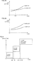
3A ist ein Diagramm, das eine Beziehung zwischen der Größe eines Gesamtstroms, der durch die IGBTs im eingeschalteten Zustand fließt, und der Größe eines Einschaltverlusts zeigt. 3A FIG. 15 is a graph showing a relationship between the magnitude of a total current flowing through the IGBTs in the on state and the magnitude of a power-on loss.
3B ist ein Diagramm, das eine Beziehung zwischen der Größe eines Gesamtstroms, der durch die IGBTs im eingeschalteten Zustand fließt, und der Größe eines Ausschaltverlusts zeigt. 3B FIG. 12 is a graph showing a relationship between the magnitude of a total current flowing through the IGBTs in the on state and the size of a turn-off loss.
4 ist ein Diagramm zum Darstellen des Konzepts der Zeitablaufsteuerung, wenn die IGBTs ausgeschaltet werden. 4 Fig. 10 is a diagram for illustrating the concept of the timing control when the IGBTs are turned off.
5 ist ein Diagramm, das eine Beziehung zwischen einem Schaltverlust und einem Kollektorstrom des IGBT zeigt. 5 FIG. 15 is a graph showing a relationship between a switching loss and a collector current of the IGBT.
6 ist ein Diagramm, das eine Beziehung zwischen einem Schaltverlust und einem Gatewiderstand des IGBT zeigt. 6 FIG. 15 is a diagram showing a relationship between a switching loss and a gate resistance of the IGBT.
7 ist ein Diagramm, das eine Beziehung zwischen einer Kollektorstromdichte und einer Sättigungsspannung zeigt. 7 FIG. 15 is a diagram showing a relationship between a collector current density and a saturation voltage.
8 ist ein Diagramm, das eine Beziehung zwischen einem Ausschaltverlust und einer Sättigungsspannung zeigt. 8th Fig. 15 is a diagram showing a relationship between a turn-off loss and a saturation voltage.
9 ist ein Diagramm, das eine Beziehung zwischen einem Kollektorstrom und einem Einschaltverlust zeigt. 9 Fig. 15 is a diagram showing a relation between a collector current and a turn-on loss.
10 ist ein Diagramm, das ein Simulationsergebnis zeigt, wenn parallel geschaltete IGBTs nacheinander geschaltet werden. 10 is a diagram showing a simulation result when IGBTs connected in parallel are switched one after the other.
11 ist eine vergrößerte Ansicht von 10 zur Zeit des Einschaltens. 11 is an enlarged view of 10 at the time of switching on.
12 ist eine vergrößerte Ansicht von 10 zur Zeit des Ausschaltens. 12 is an enlarged view of 10 at the time of switching off.
13 ist ein Diagramm, das ein Simulationsergebnis zeigt, wenn das Einschalten der parallel geschalteten IGBTs gleichzeitig durchgeführt wird und das Ausschalten nacheinander durchgeführt wird. 13 FIG. 13 is a diagram showing a simulation result when the switching-on of the parallel-connected IGBTs is simultaneously performed and the turn-off is performed sequentially.
14 ist eine vergrößerte Ansicht von 13 zur Zeit des Einschaltens. 14 is an enlarged view of 13 at the time of switching on.
15 ist eine vergrößerte Ansicht von 13 zur Zeit des Ausschaltens. 15 is an enlarged view of 13 at the time of switching off.
16A ist ein Diagramm, das eine Beziehung zwischen einem Gesamtstrom, der durch die parallel geschalteten IGBTs fließt, und einem Einschaltverlust zeigt. 16A FIG. 15 is a diagram showing a relationship between a total current flowing through the parallel-connected IGBTs and a turn-on loss.
16B ist eine vergrößerte Ansicht eines Abschnitts in einem Rahmen, der in 16A durch eine gestrichelte Linie gezeigt ist. 16B is an enlarged view of a portion in a frame that is in 16A shown by a dashed line.
17 ist ein Schaltbild eines Aufbaus einer Leistungshalbleitervorrichtung gemäß einer zweiten Ausführungsform. 17 FIG. 12 is a circuit diagram showing a structure of a power semiconductor device according to a second embodiment. FIG.
18 ist ein Diagramm, das ein Beispiel für ein Zeitverlaufsdiagramm eines Steuersignals zeigt, das von einer in 17 gezeigten integrierten Schaltung ausgegeben wird. 18 FIG. 15 is a diagram showing an example of a timing chart of a control signal that is different from an in 17 shown integrated circuit is output.
19 ist ein Schaltbild eines Aufbaus einer Leistungshalbleitervorrichtung gemäß einer dritten Ausführungsform. 19 FIG. 12 is a circuit diagram showing a structure of a power semiconductor device according to a third embodiment. FIG.
20 ist ein Diagramm, das ein Beispiel für ein Zeitverlaufsdiagramm eines Steuersignals zeigt, das von einer in 19 gezeigten integrierten Schaltung ausgegeben wird. 20 FIG. 15 is a diagram showing an example of a timing chart of a control signal that is different from an in 19 shown integrated circuit is output.
21 ist ein Schaltbild eines Aufbaus einer Leistungshalbleitervorrichtung gemäß einer vierten Ausführungsform. 21 FIG. 15 is a circuit diagram showing a structure of a power semiconductor device according to a fourth embodiment. FIG.
22 ist ein Schaltbild eines Aufbaus einer Leistungshalbleitervorrichtung gemäß einer fünften Ausführungsform. 22 FIG. 15 is a circuit diagram showing a structure of a power semiconductor device according to a fifth embodiment. FIG.
23 ist ein Diagramm, das ein Beispiel für ein Zeitverlaufsdiagramm eines Steuersignals zeigt, das von einer in 22 gezeigten integrierten Schaltung ausgegeben wird. 23 FIG. 15 is a diagram showing an example of a timing chart of a control signal that is different from an in 22 shown integrated circuit is output.
24 ist ein Schaltbild eines Aufbaus einer Leistungshalbleitervorrichtung gemäß einer sechsten Ausführungsform. 24 FIG. 10 is a circuit diagram showing a structure of a power semiconductor device according to a sixth embodiment. FIG.
25 ist ein Schaltbild eines Aufbaus einer Leistungshalbleitervorrichtung gemäß einer siebten Ausführungsform. 25 FIG. 10 is a circuit diagram showing a structure of a power semiconductor device according to a seventh embodiment. FIG.
26 ist ein Schaltbild eines Aufbaus einer Leistungshalbleitervorrichtung gemäß einer achten Ausführungsform. 26 FIG. 12 is a circuit diagram showing a structure of a power semiconductor device according to an eighth embodiment. FIG.
27 ist ein Schaltbild eines Aufbaus einer Leistungshalbleitervorrichtung gemäß einer neunten Ausführungsform. 27 FIG. 10 is a circuit diagram showing a structure of a power semiconductor device according to a ninth embodiment. FIG.
28 ist ein Diagramm, das ein Beispiel für ein Zeitverlaufsdiagramm eines Steuersignals zeigt, das von einer in 27 gezeigten integrierten Schaltung ausgegeben wird. 28 FIG. 15 is a diagram showing an example of a timing chart of a control signal that is different from an in 27 shown integrated circuit is output.
29 ist ein Schaltbild eines Aufbaus einer Leistungshalbleitervorrichtung gemäß einer zehnten Ausführungsform. 29 FIG. 12 is a circuit diagram showing a structure of a power semiconductor device according to a tenth embodiment. FIG.
30 ist ein Schaltbild eines Aufbaus einer Leistungshalbleitervorrichtung gemäß einer elften Ausführungsform. 30 FIG. 15 is a circuit diagram showing a structure of a power semiconductor device according to an eleventh embodiment. FIG.
31 ist ein Diagramm zum Darstellen von Spezifikationen von IGBTs, die in einer Leistungshalbleitervorrichtung gemäß einer zwölften Ausführungsform enthalten sind. 31 FIG. 15 is a diagram for illustrating specifications of IGBTs included in a power semiconductor device according to a twelfth embodiment. FIG.
32 ist ein Schaltbild eines Aufbaus einer Leistungshalbleitervorrichtung gemäß einer Abwandlung einer dreizehnten Ausführungsform. 32 FIG. 15 is a circuit diagram showing a structure of a power semiconductor device according to a modification of a thirteenth embodiment. FIG.
33 ist ein Diagramm, das für eine vierzehnte Ausführungsform eine Abwandlung des Steuerns des Schaltens der IGBTs durch Triebersteuereinheiten in den Leistungshalbleitervorrichtung gemäß der zweiten, neunten und zehnten Ausführungsform zeigt. 33 FIG. 15 is a diagram showing, for a fourteenth embodiment, a modification of controlling the switching of the IGBTs by driver control units in the power semiconductor device according to the second, ninth, and tenth embodiments.
34 ist ein Diagramm, das für eine fünfzehnte Ausführungsform eine Abwandlung des Steuerns des Schaltens der IGBTs durch Triebersteuereinheiten in den Leistungshalbleitervorrichtung gemäß der fünften und elften Ausführungsform zeigt. 34 FIG. 15 is a diagram showing, for a fifteenth embodiment, a modification of controlling the switching of the IGBTs by driver control units in the power semiconductor device according to the fifth and eleventh embodiments.
35 ist ein Diagramm, das für eine sechzehnte Ausführungsform eine weitere Abwandlung des Steuerns des Schaltens der IGBTs durch Triebersteuereinheiten in den Leistungshalbleitervorrichtung gemäß der zweiten, neunten und zehnten Ausführungsform zeigt. 35 FIG. 15 is a diagram showing, for a sixteenth embodiment, another modification of controlling the switching of the IGBTs by driver control units in the power semiconductor device according to the second, ninth, and tenth embodiments.
36 ist ein Schaltbild eines Aufbaus einer Leistungshalbleitervorrichtung gemäß einer neunzehnten Ausführungsform. 36 FIG. 15 is a circuit diagram showing a structure of a power semiconductor device according to a nineteenth embodiment. FIG.
37A ist ein Diagramm, das ein Beispiel für einen Signalverlauf zeigt, der von einem in 36 gezeigten Stromerfassungssensor ausgegeben wird, wenn eine Ausgabe des Stromerfassungssensors nicht eine Referenzspannung überschreitet, die einem Schwellenwert entspricht. 37A FIG. 13 is a diagram showing an example of a waveform that is different from an in 36 current detection sensor is output when an output of the current detection sensor does not exceed a reference voltage corresponding to a threshold value.
37B ist ein Diagramm, das ein Beispiel für einen Signalverlauf zeigt, der von einem in 36 gezeigten Stromerfassungssensor ausgegeben wird, wenn eine Ausgabe des Stromerfassungssensors die Referenzspannung überschreitet, die dem Schwellenwert entspricht. 37B FIG. 13 is a diagram showing an example of a waveform that is different from an in 36 shown current detection sensor is output when an output of the current detection sensor exceeds the reference voltage, which corresponds to the threshold value.
38 ist ein Schaltbild eines Aufbaus einer Leistungshalbleitervorrichtung gemäß einer zwanzigsten Ausführungsform. 38 FIG. 15 is a circuit diagram showing a structure of a power semiconductor device according to a twentieth embodiment. FIG.
39 ist ein Schaltbild eines Aufbaus einer Leistungshalbleitervorrichtung gemäß einer einundzwanzigsten Ausführungsform. 39 FIG. 15 is a circuit diagram showing a structure of a power semiconductor device according to a twenty-first embodiment. FIG.
40 ist ein Schaltbild eines Aufbaus einer Leistungshalbleitervorrichtung gemäß einer zweiundzwanzigsten Ausführungsform. 40 FIG. 10 is a circuit diagram showing a structure of a power semiconductor device according to a twenty-second embodiment. FIG.
Mit Bezug auf die Zeichnungen werden im folgenden Ausführungsformen von Leistungshalbleitervorrichtungen im Detail beschrieben. Davon sind die in der ersten bis achten Ausführungsform beschriebenen Leistungshalbleitervorrichtungen keine Leistungshalbleitervorrichtungen gemäß der vorliegenden Erfindung, weil ihnen der beanspruchte Stromerfassungsabschnitt fehlt. Sie beschreiben jedoch bereits Merkmale der erfindungsgemäßen Ausführungsformen und dienen daher als Erläuterungsbeispiele zum besseren Verständnis der vorliegenden Erfindung.Embodiments of power semiconductor devices will be described in detail below with reference to the drawings. Of these, the power semiconductor devices described in the first to eighth embodiments are not power semiconductor devices according to the present invention because they lack the claimed current detecting portion. However, they already describe features of the embodiments according to the invention and therefore serve as illustrative examples for a better understanding of the present invention.
Es sei angemerkt, dass dieselben oder einander entsprechende Elemente durch dieselben Bezugszeichen gekennzeichnet sind und ihre Beschreibung nicht wiederholt wird. It should be noted that the same or corresponding elements are denoted by the same reference numerals and their description will not be repeated.
1 ist ein Diagramm eines Aufbaus einer Leistungshalbleitervorrichtung gemäß einer ersten Ausführungsform. Mit Bezug auf 1 enthält die Leistungshalbleitervorrichtung 200 die Leistungshalbleiterelemente Q1 und Q2, die parallel zueinander zwischen einen Hochspannungsknoten HV und einen Masseknoten GND geschaltet sind, und eine Treibersteuereinheit 100. Auch wenn in 1 als Beispiel ein IGBT als Leistungshalbleiterelement Q1, Q2 dargestellt ist, können auch andere Halbleiterelemente wie z. B. ein Leistungs-MOSFET oder ein Bipolartransistor verwendet werden. Die Leistungshalbleiterelemente Q1, Q2 werden im folgenden jeweils auch als IGBTs Q1, Q2 bezeichnet. Der Hochspannungsknoten HV, mit dem die Kollektoren der IGBTs Q1, Q2 jeweils verbunden sind, ist mit der zu steuernden elektrischen Einrichtung verbunden, und eine hohe Spannung liegt an ihm an. 1 FIG. 10 is a diagram of a configuration of a power semiconductor device according to a first embodiment. FIG. Regarding 1 contains the power semiconductor device 200 the power semiconductor elements Q1 and Q2, which are connected in parallel with each other between a high voltage node HV and a ground node GND, and a driver control unit 100 , Even if in 1 As an example, an IGBT is shown as a power semiconductor element Q1, Q2, other semiconductor elements such. As a power MOSFET or a bipolar transistor can be used. The power semiconductor elements Q1, Q2 will be hereinafter referred to as IGBTs Q1, Q2, respectively. The high voltage node HV, to which the collectors of the IGBTs Q1, Q2 are respectively connected, is connected to the electrical device to be controlled, and a high voltage is applied to it.
Die Treibersteuerschaltung 100 schaltet die IGBTs Q1, Q2 in Übereinstimmung mit einem Logikpegel eines von außen empfangenen Treibersignals DS ein oder aus. In dieser Ausführungsform wird angenommen, dass die Treibersteuereinheit 100 die Leistungshalbleiterelemente Q1, Q2 einschaltet, wenn sie das Treibersignal DS auf einem hohen Pegel (H-Pegel) empfängt, und dass sie die Leistungshalbleiterelemente Q1, Q2 ausschaltet, wenn sie das Treibersignal DS auf einem niedrigen Pegel (L-Pegel) empfängt. Das Treibersignal DS auf H-Pegel wird auch als Einschaltbefehl bezeichnet, während das Treibersignal DS auf L-Pegel auch als Ausschaltbefehl bezeichnet wird. Der Einschaltbefehl und der Ausschaltbefehl werden der Treibersteuereinheit 100 abwechselnd und wiederholt zugeführt. Ein bestimmtes Aufbaubeispiel der Treibersteuereinheit 100 wird in der zweiten und den folgenden Ausführungsformen beschrieben.The driver control circuit 100 turns on / off the IGBTs Q1, Q2 in accordance with a logic level of a driver signal DS received from the outside. In this embodiment, it is assumed that the driver control unit 100 the power semiconductor elements Q1, Q2 turns on when receiving the drive signal DS at a high level (H level), and turns off the power semiconductor elements Q1, Q2 when receiving the drive signal DS at a low level (L level). The H-level drive signal DS is also called the turn-on command, and the L-level drive signal DS is also called the turn-off command. The turn-on command and the turn-off command become the driver control unit 100 fed alternately and repeatedly. A specific construction example of the driver control unit 100 is described in the second and following embodiments.
2A–2C sind Zeitverlaufsdiagramme, die eine Beziehung zwischen dem Treibersignal DS und den Gatespannungen der Leistungshalbleiterelemente Q1, Q2 zeigen. Mit Bezug auf 1 und 2A–2C kann die Treibersteuereinheit 100, wenn sie den Einschaltbefehl empfängt und die IGBTs Q1, Q2 einschaltet, zwischen einem Fall, in dem die IGBTs Q1, Q2 gleichzeitig eingeschaltet werden, und einem Fall, in dem einer der IGBTs Q1, Q2 (beispielsweise IGBT Q1) zuerst eingeschaltet wird und dann der andere IGBT eingeschaltet wird, umschalten. Wenn die Treibersteuereinheit 100 den Ausschaltbefehl erhält und die IGBTs Q1, Q2 ausschaltet, kann sie außerdem zwischen einem Fall, in dem die IGBTs Q1, Q2 gleichzeitig ausgeschaltet werden, und einem Fall, in dem einer der IGBTs Q1, Q2 (beispielsweise der IGBT Q1) zuerst ausgeschaltet wird und danach der andere IGBT ausgeschaltet wird, umschalten. Ob die IGBTs Q1, Q2 gleichzeitig geschaltet werden sollen oder ob sie unabhängig voneinander zu unterschiedlichen Zeiten geschaltet werden sollen, kann bestimmt werden basierend auf der Größe der Hauptströme I1, I2 oder des Gesamtstrom It, der eine Kombination der Hauptströme I1 und I2 ist, die jeweils durch die IGBTs Q1, Q2 fließen, wenn die IGBTs Q1, Q2 als Reaktion auf den Einschaltbefehl eingeschaltet (leitend) sind. Insbesondere ist in der ersten Ausführungsform der Gesamtstrom It, der durch die Halbleiterleistungselemente Q1, Q2 fließt, basierend auf seiner Größe in drei Bereiche eingeteilt. 2A - 2C Fig. 15 are timing charts showing a relationship between the drive signal DS and the gate voltages of the power semiconductor elements Q1, Q2. Regarding 1 and 2A - 2C can the driver control unit 100 when receiving the turn-on command and turning on the IGBTs Q1, Q2, between a case where the IGBTs Q1, Q2 are simultaneously turned on and a case where one of the IGBTs Q1, Q2 (eg, IGBT Q1) is first turned on and then the other IGBT is turned on, toggle. If the driver control unit 100 receives the turn-off command and turns off the IGBTs Q1, Q2, it may also be turned off between a case where the IGBTs Q1, Q2 are simultaneously turned off and a case where one of the IGBTs Q1, Q2 (eg, the IGBT Q1) is turned off first and then the other IGBT is turned off, toggle. Whether the IGBTs Q1, Q2 are to be switched simultaneously or whether they are to be independently switched at different times may be determined based on the magnitude of the main currents I1, I2 or the total current It, which is a combination of the main currents I1 and I2 respectively through the IGBTs Q1, Q2 when the IGBTs Q1, Q2 are turned on (conducting) in response to the turn-on command. More specifically, in the first embodiment, the total current It flowing through the semiconductor power elements Q1, Q2 is divided into three areas based on its size.
2A zeigt einen Fall, in dem die Größe des Gesamtstroms It relativ klein ist. Wenn das Treibersignal S zum Zeitpunkt t1 vom L-Pegel zum H-Pegel wechselt, schaltet die Treibersteuereinheit 100 den IGBT Q1 ein, indem sie eine Spannung auf H-Pegel an das Gate des IGBT Q1 anlegt. Zu einem nachfolgenden Zeitpunkt t2 schaltet die Treibersteuereinheit 100 den IGBT Q2 ein durch Anlegen einer Spannung auf H-Pegel an das Gate des IGBT Q2. Wenn das Treibersignal DS zum Zeitpunkt t3 vom H-Pegel zum L-Pegel wechselt, schaltet die Treibersteuereinheit 100 den IGBT Q1 aus durch Anlegen einer Spannung auf L-Pegel an das Gate des IGBT Q1. Zu einem nachfolgenden Zeitpunkt t4 schaltet die Treibersteuereinheit 100 den IGBT Q2 aus durch Anlegen einer Spannung auf L-Pegel an das Gate des IGBT Q2. Daher wird beim Einschalten ein Schaltverlust (Einschaltverlust Eon) hauptsächlich in dem IGBT Q1 bewirkt, der zuerst eingeschaltet wird, während beim Ausschalten ein Schaltverlust (Ausschaltverlust Eoff) hauptsächlich in dem IGBT Q2 bewirkt wird, der nachfolgend ausgeschaltet wird. 2A shows a case where the size of the total current It is relatively small. When the drive signal S changes from the L level to the H level at time t1, the drive control unit switches 100 IGBT Q1 by applying an H-level voltage to the gate of the IGBT Q1. At a subsequent time t2, the driver control unit switches 100 the IGBT Q2 by applying a voltage to H level to the gate of the IGBT Q2. When the drive signal DS changes from H level to L level at time t3, the drive control unit switches 100 the IGBT Q1 by applying a voltage to L level to the gate of the IGBT Q1. At a subsequent time t4, the driver control unit switches 100 the IGBT Q2 by applying a voltage to L level to the gate of the IGBT Q2. Therefore, on turn-on, a switching loss (turn-on loss Eon) is mainly caused in the IGBT Q1 turned on first, while a turn-off loss (turn-off loss Eoff) is mainly caused in the IGBT Q2 which is subsequently turned off when turned off.
2B zeigt einen Fall, in dem die Größe des Gesamtstroms It mittelgroß ist. Wenn das Treibersignal DS zum Zeitpunkt t1 vom L-Pegel zum H-Pegel wechselt, schaltet die Treibersteuereinheit 100 hierbei die IGBTs Q1, Q2 gleichzeitig ein durch Anlegen einer Spannung auf H-Pegel an die Gates beider IGBTs Q1, Q2. Wenn das Treibersignal DS zum Zeitpunkt t3 vom H-Pegel zum L-Pegel wechselt, schaltet die Treibersteuereinheit 100 den IGBT Q1 aus durch Anlegen einer Spannung auf L-Pegel an das Gate des IGBT Q1. Zum nachfolgenden Zeitpunkt t4 schaltet die Treibersteuereinheit 100 den IGBT Q2 aus durch Anlegen einer Spannung auf L-Pegel an das Gate des IGBT Q2. Daher wird beim Einschalten ein Schaltverlust (Einschaltverlust Eon) in beiden IGBTs Q1, Q2 bewirkt. Beim Ausschalten wird ein Schaltverlust (Ausschaltverlust Eoff) hauptsächlich in dem IGBT Q2 bewirkt, der nachfolgend ausgeschaltet wird. 2 B shows a case where the magnitude of the total current It is medium. When the drive signal DS changes from the L level to the H level at time t1, the drive control unit switches 100 Here, the IGBTs Q1, Q2 simultaneously by applying a voltage to H level to the gates of both IGBTs Q1, Q2. When the drive signal DS changes from H level to L level at time t3, the drive control unit switches 100 the IGBT Q1 by applying a voltage to L level to the gate of the IGBT Q1. At the subsequent time t4, the driver control unit switches 100 the IGBT Q2 by applying a voltage to L level to the gate of the IGBT Q2. Therefore, at power-up, a switching loss (turn-on loss Eon) is caused in both IGBTs Q1, Q2. At turn-off, a switching loss (turn-off loss Eoff) is caused mainly in the IGBT Q2, which is subsequently turned off.
2C zeigt einen Fall, in dem die Größe des Gesamtstroms It relativ groß ist. Wenn das Treibersignal DS in diesem Fall zum Zeitpunkt t1 vom L-Pegel zum H-Pegel wechselt, schaltet die Steuereinheit 100 die IGBTs Q1, Q2 gleichzeitig an durch Anlegen einer Spannung auf H-Pegel an die Gates beider IGBTs Q1, Q2. Wenn das Treibersignal DS zum Zeitpunkt t3 vom H-Pegel zum L-Pegel wechselt, schaltet die Treibersteuereinheit 100 die IGBTs Q1, Q2 gleichzeitig aus durch Anlegen einer Spannung auf L-Pegel an die Gates beider IGBTs Q1, Q2. Daher wird sowohl beim Einschalten als auch beim Ausschalten ein Schaltverlust in beiden IGBTs Q1, Q2 bewirkt. 2C shows a case where the size of the total current It is relatively large. In this case, when the drive signal DS changes from the L level to the H level at time t1, the control unit turns on 100 the IGBTs Q1, Q2 simultaneously by applying a voltage at H level to the gates of both IGBTs Q1, Q2. When the drive signal DS changes from H level to L level at time t3, the drive control unit switches 100 the IGBTs Q1, Q2 simultaneously by applying a voltage to L level to the gates of both IGBTs Q1, Q2. Therefore, both switching on and off, switching loss is caused in both IGBTs Q1, Q2.
Auch wenn in der obigen Beschreibung beim aufeinanderfolgenden Schalten der IGBTs Q1, Q2 zu unterschiedlichen Zeitpunkten der IGBT Q1 früher ein- oder ausgeschaltet wird als der IGBT Q2, kann ein beliebiger von ihnen zuerst geschaltet werden, wenn die IGBTs Q1, Q2 identische Eigenschaften haben.Although, in the above description, when the IGBTs Q1, Q2 are successively switched on or off at different times, the IGBT Q1 turns on or off earlier than the IGBT Q2, any one of them may be switched first when the IGBTs Q1, Q2 have identical characteristics.
Es werden nun die Gründe beschrieben, warum das Schalten der IGBTs Q1, Q2 mit dem obigen Verfahren gesteuert wird.The reasons why the switching of the IGBTs Q1, Q2 is controlled by the above method will now be described.
3A ist ein Diagramm, das eine Beziehung zwischen der Größe des Gesamtstroms It, der durch die IGBTs Q1, Q2 im eingeschalteten Zustand fließt, und der Größe eines Einschaltverlusts Eon zeigt. 3B ist ein Diagramm, das eine Beziehung zwischen der Größe eines Gesamtstroms, der durch die IGBTs im eingeschalteten Zustand fließt, und der Größe eines Ausschaltverlusts Eoff zeigt. In 3A und 3B sind der Einschaltverlust Eon und der Ausschaltverlust Eoff als elektrische Leistung in mJ angegeben, die pro Puls des Treibersignals DS verbraucht wird. Ein Fall, in dem die IGBTs Q1, Q2 jeweils alleine mit unterschiedlichem Zeitablauf geschaltet werden, ist als ”1 CHIP” (1P) bezeichnet, während ein Fall, in dem die IGBTs Q1, Q2 gleichzeitig geschaltet werden als ”2 CHIP” (2P) bezeichnet ist. 3A FIG. 15 is a graph showing a relationship between the magnitude of the total current It flowing through the IGBTs Q1, Q2 in the on state and the magnitude of a turn-on loss Eon. 3B FIG. 15 is a graph showing a relationship between the magnitude of a total current flowing through the IGBTs in the on state and the magnitude of a turn-off loss Eoff. In 3A and 3B For example, the turn-on loss Eon and the turn-off loss Eoff are indicated as electric power in mJ consumed per pulse of the drive signal DS. A case where the IGBTs Q1, Q2 are each switched alone with different timing is designated as "1 CHIP" (1P), while a case where the IGBTs Q1, Q2 are switched simultaneously as "2 CHIP" (2P ).
Mit Bezug auf 3A führt das Einschalten der IGBTs Q1, Q2 alleine mit unterschiedlichem Zeitablauf, wenn der Gesamtstrom It, der durch die IGBTs Q1, Q2 fließt, kleiner als ein bestimmter Schwellenwert Ith1 ist, zu einem geringeren Einschaltverlust Eon als in einem Fall, in dem die IGBTs Q1, Q2 gleichzeitig eingeschaltet werden. In einem Fall, in dem der Gesamtstrom größer als der Schwellenwert Ith1 ist, führt das gleichzeitige Einschalten der IGBTs Q1, Q2 zu einem geringeren Einschaltverlust Eon als in einem Fall, in dem die IGBTs Q1, Q2 jeweils alleine eingeschaltet werden. Wenn der Gesamtstrom kleiner gleich dem Schwellenwert Ith1 ist, schaltet die Treibersteuereinheit 100 in 1 deshalb zuerst den IGBT Q1 an, und anschließend schaltet sie den IGBT Q2 an, wie es in 2A gezeigt ist. Wenn der Gesamtstrom It größer als der Schwellenwert Ith1 ist, schaltet die Treibersteuereinheit 100 die IGBTs Q1, Q2 gleichzeitig an, wie es in 2B gezeigt ist. Somit kann der Einschaltverlust Eon verglichen mit dem herkömmlichen Beispiel verringert werden.Regarding 3A For example, if the total current It flowing through the IGBTs Q1, Q2 is less than a predetermined threshold value Ith1, turning on the IGBTs Q1, Q2 alone with different timing results in a smaller turn-on loss Eon than in a case where the IGBTs Q1 , Q2 be turned on at the same time. In a case where the total current is greater than the threshold value Ith1, the simultaneous turn-on of the IGBTs Q1, Q2 results in a lower turn-on loss Eon than in a case where the IGBTs Q1, Q2 are turned on alone respectively. If the total current is less than or equal to the threshold Ith1, the driver control unit switches 100 in 1 Therefore, first turn on the IGBT Q1, and then turn on the IGBT Q2 as shown in 2A is shown. When the total current It is greater than the threshold Ith1, the driver control unit turns on 100 the IGBTs Q1, Q2 at the same time as it is in 2 B is shown. Thus, the turn-on loss Eon can be reduced as compared with the conventional example.
Mit Bezug auf 3B führt im Fall des Ausschaltverlusts Eoff das gleichzeitige Ausschalten der IGBT Q1, Q2 mit unterschiedlichen Zeitabläufen unabhängig von der Größe des Gesamtstroms It, der durch die IGBTs Q1, Q2 im leitenden Zustand fließt, zu einem kleineren Ausschaltverlust als in einem Fall, in dem sie gleichzeitig eingeschaltet werden. Wie in 2A und 2B gezeigt, schaltet die Treibersteuereinheit 100 in 1 daher zuerst den IGBT Q1 ein, und anschließend schaltet sie den IGBT Q2 ein. Somit kann der Ausschaltverlust Eoff verglichen mit einem Fall, in dem die IGBTs Q1, Q2 gleichzeitig eingeschaltet werden, verringert werden.Regarding 3B In the case of the turn-off loss Eoff, simultaneously turning off the IGBTs Q1, Q2 at different timings regardless of the magnitude of the total current It flowing through the IGBTs Q1, Q2 in the conductive state results in a smaller turn-off loss than in a case where they simultaneously be turned on. As in 2A and 2 B shown, turns on the driver control unit 100 in 1 Therefore, first IGBT Q1, and then it turns on the IGBT Q2. Thus, the turn-off loss Eoff can be reduced as compared with a case where the IGBTs Q1, Q2 are simultaneously turned on.
Es sei angemerkt, dass in einem Fall, in dem die IGBTs Q1, Q2 jeweils alleine ausgeschaltet werden, der Gesamtstrom It, der durch die IGBTs Q1, Q2 fließt, wenn er den Maximalwert pro Element überschreitet, ein Element zerstören kann, das nachfolgend ausgeschaltet wird. Um den Durchbruch eines Elements zu verhindern, werden die IGBTs Q1, Q2 dann, wenn der Gesamtstrom It nahe dem Maximalwert pro Element ist, gleichzeitig ausgeschaltet, wie es in 2C gezeigt ist.It should be noted that, in a case where the IGBTs Q1, Q2 are each turned off alone, the total current It flowing through the IGBTs Q1, Q2, if it exceeds the maximum value per element, may destroy an element that subsequently turns off becomes. In order to prevent the breakdown of an element, when the total current It is close to the maximum value per element, the IGBTs Q1, Q2 are simultaneously turned off, as shown in FIG 2C is shown.
4 ist ein Diagramm zum Darstellen eines Konzepts der Zeitablaufsteuerung beim Ausschalten der IGBTs Q1, Q2. 4 FIG. 15 is a diagram for illustrating a concept of the timing when turning off the IGBTs Q1, Q2.
In Bezug auf 4 wird der genannte Maximalwert eines Hauptstroms pro Element der IGBTs Q1, Q2 als IR angenommen. Ein Schwellenwert Ith2 wird auf einen Wert eingestellt, der geringfügig kleiner ist als der angegebene Maximalwert IR, und ein Schwellenwert Ith3 wird auf einen Wert gesetzt, der geringfügig kleiner ist als das Zweifache des angegebenen Maximalwerts IR (2 × IR). Wenn der Gesamtstrom It, der durch die IGBTs Q1, Q2 im leitenden Zustand fließt, kleiner ist als der Schwellenwert Ith2, steuert die Treibersteuereinheit 100 in 1 die IGBTs Q1, Q2 so, dass jeder von ihnen als Reaktion auf den Ausschaltbefehl aufeinanderfolgend ausgeschaltet wird. Wenn der Gesamtstrom It größer gleich dem Schwellenwert Ith2 und kleiner gleich dem Schwellenwert Ith3 ist, steuert die Treibersteuereinheit 100 die IGBTs Q1, Q2 so, dass sie als Reaktion auf den Ausschaltbefehl gleichzeitig ausgeschaltet werden. Auch wenn verglichen mit einem Fall, in dem ein Element nachträglich ausgeschaltet wird, der Ausschaltverlust Eoff ansteigt, wird eine solche Schaltsteuerung durchgeführt zum Schutz gegen das Kurzschließen eines IGBT. Wenn der Gesamtstrom größer gleich dem Schwellenwert Ith3 ist, wird ein Schutz gegen Kurzschluss bereitgestellt zum Steuern der IGBTs Q1, Q2 so, dass sie beide unabhängig von einem Logikpegel des Treibersignals DS ausgeschaltet werden.In relation to 4 the said maximum value of one main current per element of the IGBTs Q1, Q2 is assumed to be IR. A threshold value Ith2 is set to a value slightly smaller than the specified maximum value IR, and a threshold value Ith3 is set to a value slightly smaller than twice the specified maximum value IR (2 × IR). When the total current It flowing through the IGBTs Q1, Q2 in the conductive state is smaller than the threshold value Ith2, the driver control unit controls 100 in 1 the IGBTs Q1, Q2 so that each of them is sequentially turned off in response to the turn-off command. When the total current It is equal to or greater than the threshold value Ith2 and less than the threshold value Ith3, the driver control unit controls 100 the IGBTs Q1, Q2 are turned off simultaneously in response to the turn-off command. Even if compared with a case where an element is subsequently turned off, the turn-off loss Eoff increases, such switching control is performed to protect against short-circuiting of an IGBT. If the total current is greater than or equal to the threshold Ith3, a Short-circuit protection provided for controlling the IGBTs Q1, Q2 so as to be turned off regardless of a logic level of the drive signal DS.
Es werden nun die Gründe beschrieben, warum die in 3A und 3B gezeigten Schalteigenschaften erzielt werden.The reasons why the in 3A and 3B shown switching properties can be achieved.
5 ist ein Diagramm, das eine Beziehung zwischen einem Schaltverlust und einem Kollektorstrom des IGBT zeigt. 5 zeigt in Abhängigkeit von dem Kollektorstrom Ic einen Einschaltverlust Eon, einen Ausschaltverlust Eoff und einen Schaltverlust Err bei einem Rückwärtserholungsvorgang. 6 ist ein Diagramm, das eine Beziehung zwischen einem Schaltverlust und einem Gatewiderstand des IGBT zeigt. 6 zeigt in Abhängigkeit von einem Gatewiderstand RG einen Einschaltverlust Eon, einen Ausschaltverlust Eoff, und einen Schaltverlust Err in einem Rückwärtserholungsvorgang. Die in 5 und 6 gezeigten Kennlinien sind Datenblätter eines IGBT-Moduls (Modellnummer CM600HX-24A von Mitsubishi Electric Corporation) entnommen. 5 FIG. 15 is a graph showing a relationship between a switching loss and a collector current of the IGBT. 5 shows a turn-on loss Eon, a turn-off loss Eoff, and a switching loss Err in a reverse recovery operation in response to the collector current Ic. 6 FIG. 15 is a diagram showing a relationship between a switching loss and a gate resistance of the IGBT. 6 shows a turn-on loss Eon, a turn-off loss Eoff, and a switching loss Err in a reverse recovery operation in response to a gate resistance RG. In the 5 and 6 The characteristics shown are data sheets of an IGBT module (model number CM600HX-24A from Mitsubishi Electric Corporation).
Mit Bezug auf 5 wird der Ausschaltverlust Eoff als Potenzfunktion des Kollektorstroms Ic ausgedrückt. Das bedeutet, dass der Ausschaltverlust Eoff in dem in 5 gezeigten doppeltlogarithmischen Diagramm proportional zu dem Kollektorstrom Ic ist. Wenn ein Exponent mit dem Symbol ”^”‚ bezeichnet wird, kann der Ausschaltverlust Eoff unter Verwendung von Konstanten a, b wie folgt ausgedrückt werden: Eoff = a × Ic^b (1) Regarding 5 the turn-off loss Eoff is expressed as a power function of the collector current Ic. This means that the switch-off loss Eoff in the in 5 is a log-log diagram proportional to the collector current Ic. When an exponent is denoted by the symbol "^", the turn-off loss Eoff can be expressed using constants a, b as follows: Eoff = a × Ic ^ b (1)
Wenn ein Strom, der durch jeden der IGBTs Q1, Q2 in 1 fließt, als Io [in A] bezeichnet wird, wird der Ausschaltverlust Eoff_1P, wenn die Elemente einzeln ausgeschaltet werden, wie folgt ausgedrückt: Eoff_1P = a × (2 × Io)^b (2) When a current flowing through each of the IGBTs Q1, Q2 in 1 when Io [in A] is called, the turn-off loss Eoff_1P when the elements are turned off one by one is expressed as follows: Eoff_1P = a × (2 × Io) ^ b (2)
Der Ausschaltverlust Eoff_2P, wenn zwei Elemente gleichzeitig ausgeschaltet werden, wird wie folgt ausgedrückt: Eoff_2P = 2 × a × Io^b (3) The switch-off loss Eoff_2P when two elements are switched off simultaneously is expressed as follows: Eoff_2P = 2 × a × Io ^ b (3)
Ein Verhältnis zwischen den obigen Gleichungen (2) und (3) wird wie folgt ausgedrückt: Eoff_1P/Eoff_2P = 2^(b – 1) (4) A relationship between the above equations (2) and (3) is expressed as follows: Eoff_1P / Eoff_2P = 2 ^ (b - 1) (4)
Wenn b < 1, ist die unten gezeigte Beziehung erfüllt: Eoff_1P < Eoff_2P (5) If b <1, the relationship shown below is satisfied: Eoff_1P <Eoff_2P (5)
Die Beziehung b < 1 bedeutet, dass eine Steigung des Graphen in 5 kleiner 1 ist, und diese Beziehung b < 1 ist normalerweise erfüllt.The relationship b <1 means that a slope of the graph in 5 is less than 1, and this relationship b <1 is normally satisfied.
Unter Verwendung eines spezifischen Zahlenwerts wird eine Verifizierung durchgeführt. Es sei angenommen, dass ein Hauptstrom von 200 A pro Element durch die in 1 gezeigten IGBTs Q1, Q2 fließt, d. h. I1 = I2 = 200 A. Der Gesamtstrom It ist dann 400 A. In Bezug auf 5 ist der Ausschaltverlust, wenn der Kollektorstrom 200 A beträgt, etwa 41 mJ/Puls, und wenn der Kollektorstrom 400 A beträgt, ist der Ausschaltverlust Eoff etwa 62 mJ/Puls. Daher beträgt der Ausschalterlust Eoff, wenn zwei Elemente gleichzeitig ausgeschaltet werden, 82 mJ/Puls insgesamt, während der Ausschaltverlust Eoff, wenn die Elemente einzeln ausgeschaltet werden, 62 mJ/Puls beträgt, weil der Verlust in einem Element erzeugt wird, das nachträglich ausgeschaltet wird. Somit führt das einzelne Ausschalten der Elemente zu einem geringeren Ausschaltverlust Eoff.Using a specific numerical value, verification is performed. It is assumed that a main current of 200 A per element by the in 1 IGBTs Q1, Q2 flows, ie I1 = I2 = 200 A. The total current It is then 400 A. In relation to 5 For example, the turn-off loss when the collector current is 200 A is about 41 mJ / pulse, and when the collector current is 400 A, the turn-off loss Eoff is about 62 mJ / pulse. Therefore, the turn-off loss Eoff when two elements are turned off simultaneously is 82 mJ / pulse in total, while the turn-off loss Eoff when the elements are turned off one by one is 62 mJ / pulse because the loss is generated in an element that is subsequently turned off , Thus, turning off the elements one at a time results in less turn-off loss Eoff.
Hinsichtlich des Ausschaltverlusts Eoff sei angemerkt, dass der Ausschaltverlust Eoff wie in 6 gezeigt kaum von dem Gatewiderstand RG abhängt, und es ist zu sehen, dass die Eigenschaften des Ausschaltverlusts Eoff im Wesentlichen durch die Elementeigenschaften eines IGBT bestimmt sind. Die obigen Ergebnisse können qualitativ wie folgt betrachtet werden. 7 ist ein Diagramm, das eine Beziehung zwischen einer Kollektorstromdichte Jc und einer Sättigungsspannung VCE(sat) zeigt. Mit Bezug auf 7 sei angemerkt, dass IGBTs Q1, Q2 mit identischen Eigenschaften und identischer Größe parallel geschaltet sind. Beim einzelnen Ausschalten eines Chips (1P) ist eine Querschnittsfläche eines Abschnitts, durch die ein Hauptstrom fließt, halb so groß wie in einem Fall, in dem zwei Chips gleichzeitig ausgeschaltet werden (2P), und daher ist die Kollektorstromdichte Jc für einen Chip doppelt so groß. Wenn die Kollektorstromdichte Jc steigt, steigt die Sättigungsspannung VCE(sat).With regard to the switch-off loss Eoff it should be noted that the switch-off loss Eoff as in 6 is hardly dependent on the gate resistance RG, and it can be seen that the characteristics of the turn-off loss Eoff are substantially determined by the element characteristics of an IGBT. The above results can be qualitatively considered as follows. 7 Fig. 15 is a diagram showing a relationship between a collector current density Jc and a saturation voltage VCE (sat). Regarding 7 It should be noted that IGBTs Q1, Q2 are connected in parallel with identical characteristics and identical size. In a single turn-off of a chip (1P), a cross-sectional area of a portion through which a main current flows is half as large as in a case where two chips are simultaneously turned off (2P), and therefore the collector current density Jc for a chip is twice as large. As the collector current density Jc increases, the saturation voltage VCE (sat) increases.
8 ist ein Diagramm, das eine Beziehung zwischen einem Ausschaltverlust Eoff und der Sättigungsspannung VCE(sat) zeigt. Mit Bezug auf 8 genügen bei einem Bipolarelement der Ausschaltverlust Eoff und die Sättigungsspannung VCE(sat) einer Abwägungsbeziehung. Daher ist beim einzelnen Ausschalten der Chips (1P) der Ausschaltverlust Eoff kleiner als beim gleichzeitigen Ausschalten der zwei Chips (2P). Natürlich ist der Dauerverlust, wenn die IGBTs Q1, Q2 als Reaktion auf den Einschaltbefehl leitend sind, sowohl beim aufeinanderfolgenden Ausschalten (1P) als auch beim gleichzeitigen Ausschalten (2P) derselbe. 8th FIG. 15 is a graph showing a relationship between a turn-off loss Eoff and the saturation voltage VCE (sat). Regarding 8th For a bipolar element, the turn-off loss Eoff and the saturation voltage VCE (sat) satisfy a trade-off relationship. Therefore, when the chips (1P) are turned off one by one, the turn-off loss Eoff is smaller than when the two chips (2P) are simultaneously turned off. Of course, if the IGBTs Q1, Q2 are conductive in response to the turn-on command, the steady loss will be the same both in successive turn-off (1P) and simultaneous turn-off (2P).
Mit Bezug wieder auf 5 kann der Einschaltverlust Eon im Wesentlichen als Exponentialfunktion des Kollektorstroms Ic ausgedrückt werden. In dem in 5 gezeigten doppeltlogarithmischen Diagramm erfüllen der Einschaltverlust Eon und der Kollektorstrom Ic keine direkt proportionale Beziehung. Daher kann der Einschaltverlust unter Verwendung von Konstanten a, b wie folgt dargestellt werden: Eon = a × exp(Ic × b) (6) With respect to again 5 For example, the turn-on loss Eon can be expressed substantially as an exponential function of the collector current Ic. In the in 5 shown double logarithmic diagram, the turn-on loss Eon and the collector current Ic meet no directly proportional relationship. Therefore, the turn-on loss can be represented by using constants a, b as follows: Eon = a × exp (Ic × b) (6)
In der obigen Gleichung (6) stellt ”exp(...)” eine Exponentialfunktion dar.In the above equation (6), "exp (...)" represents an exponential function.
Unter der Bezeichnung eines Stroms, der durch jeden der IGBTs Q1, Q2 in 1 fließt, als Io [a] wird der Einschaltverlust Eon_1P, wenn die Elemente einzeln eingeschaltet werden, wie folgt dargestellt: Eon_1P = a × exp(2 × Io × b) (7) Under the designation of a current flowing through each of the IGBTs Q1, Q2 in 1 flows, as Io [a], the turn-on loss Eon_1P when the elements are turned on one by one is represented as follows: Eon_1P = a × exp (2 × Io × b) (7)
Der Einschaltverlust Eon_2P, wenn zwei Elemente gleichzeitig eingeschaltet werden, wird wie folgt dargestellt: Eon_2P = 2 × a × exp(Io × b) (8) The power-on loss Eon_2P when two elements are turned on simultaneously is shown as follows: Eon_2P = 2 × a × exp (Io × b) (8)
Ein Verhältnis zwischen den Gleichungen (7) und (8) wird wie folgt dargestellt: Eon_1P/Eon_2P = exp(Io × b)/2 (9) A relationship between equations (7) and (8) is represented as follows: Eon_1P / Eon_2P = exp (Io × b) / 2 (9)
Deshalb ist in einem Bereich eines relativ niedrigen Stroms, wo die Beziehung Io < b × ln(2) erfüllt, wobei in einen natürlichen Logarithmus darstellt, die folgende Beziehung erfüllt: Eon_1P < Eon_2P (10) Therefore, in a region of a relatively low current where the relation satisfies Io <b × In (2), representing a natural logarithm, it satisfies the following relation: Eon_1P <Eon_2P (10)
In einem Bereich eines relativ großen Stroms, in dem die Beziehung Io > b × ln(2) erfüllt ist, ist die folgende Beziehung erfüllt: Eon_1P > Eon_2P (11) In a region of a relatively large current in which the relation Io> b × In (2) is satisfied, the following relationship is satisfied: Eon_1P> Eon_2P (11)
9 ist ein Diagramm, das eine Beziehung zwischen dem Kollektorstrom Ic und dem Einschaltverlust Eon des IGBT zeigt. Mit Bezug auf 9 sei angenommen, dass ein Kollektorstrom Io durch jeden der parallel geschalteten IGBTs Q1, Q2 im eingeschalteten Zustand fließt, und der Einschaltverlust Eon, der dem Kollektorstrom Io entspricht, wird als Eo in mJ/Puls bezeichnet. Daher ist der Einschaltverlust Eon beim gleichzeitigen Einschalten von zwei Elementen 2 × Eo (ein Punkt 2P in 9). Beim aufeinanderfolgenden einzelnen Einschalten der Elemente fließt zunächst durch ein Element, das zuerst eingeschaltet wird, ein Strom von 2 × Io, und daher ist der Einschaltverlust Eon in diesem Fall Eo' (ein Punkt 1P in 9). 9 FIG. 15 is a graph showing a relationship between the collector current Ic and the turn-on loss Eon of the IGBT. Regarding 9 Assume that a collector current Io flows through each of the parallel-connected IGBTs Q1, Q2 in the on-state, and the turn-on loss Eon corresponding to the collector current Io is referred to as Eo in mJ / pulse. Therefore, the turn-on loss Eon when two elements are turned on simultaneously is 2 × Eo (a point 2P in 9 ). When the elements are successively turned on one by one, a current of 2 × Io first flows through an element which is turned on first, and therefore the turn-on loss Eon in this case is Eo '(a point 1P in FIG 9 ).
Da der Einschaltverlust Eon exponentiell mit dem Ansteigen des Kollektorstroms Ic ansteigt, ist der Verlust Eo' größer als 2 × Eo, wenn der Strom Io relativ groß ist, wie es in 9 gezeigt ist. Deshalb führt ein gleichzeitiges Einschalten von zwei Elementen zu einem niedrigeren Verlust. Wenn dagegen Io relativ klein ist, ist der Verlust Eo' kleiner als 2 × Eo. Daher führt ein aufeinanderfolgendes einzelnes Einschalten der Elemente zu einem niedrigeren Verlust.Since the turn-on loss Eon increases exponentially with the increase of the collector current Ic, the loss Eo 'is greater than 2 × Eo when the current Io is relatively large, as shown in FIG 9 is shown. Therefore, switching two elements on at the same time results in a lower loss. On the other hand, if Io is relatively small, the loss Eo 'is less than 2 × Eo. Therefore, successively turning on the elements one at a time results in a lower loss.
Es sei angemerkt, dass es nicht nur der Kollektorstrom Ic ist, der für den Einschaltverlust Eon relevant ist. Wie in 6 gezeigt, weist der Einschaltverlust Eon eine exponentielle Beziehung mit dem Gatewiderstand RG auf. Wenn der Gatewiderstand RG ansteigt, steigt nämlich der Einschaltverlust Eon exponentiell an. Außerdem sind eine Kapazität eines IGBT (eine Eingangskapazität, eine Spiegelkapazität) und Eigenschaften einer Freilaufdiode ebenso relevant für den Einschaltverlust.It should be noted that it is not only the collector current Ic relevant to the turn-on loss Eon. As in 6 1, the turn-on loss Eon has an exponential relationship with the gate resistance RG. Namely, as the gate resistance RG increases, the turn-on loss Eon increases exponentially. In addition, a capacity of an IGBT (an input capacitance, a mirror capacitance) and a free-wheeling diode characteristics are also relevant to the turn-on loss.
10–15 und 16A und 16B zeigen Simulationsergebnisse in Verbindung mit parallel geschalteten IGBTs. Bei den in 10–15 gezeigten Signalverlaufsdiagrammen sind Signalverläufe eines Verlusts in kW, eine Kollektor-Emitter-Spannung VCE in V, ein Kollektor-Emitter-Strom ICE in A und eine Gate-Emitter-Spannung VGE in V für jeden der IGBTs Q1, Q2 in dieser Reihenfolge von oben nach unten dargestellt. Der Verlust ist ein Produkt aus der Kollektor-Emitter-Spannung VCE und dem Kollektor-Emitter-Strom ICE. 10 - 15 and 16A and 16B show simulation results in connection with parallel connected IGBTs. At the in 10 - 15 The waveform diagrams shown are waveforms of a loss in kW, a collector-emitter voltage VCE in V, a collector-emitter current ICE in A, and a gate-emitter voltage VGE in V for each of the IGBTs Q1, Q2 in this order from the top shown below. The loss is a product of the collector-emitter voltage VCE and the collector-emitter current ICE.
10 ist ein Diagramm, das Simulationsergebnisse zeigt, wenn parallel geschaltete IGBTs nacheinander geschaltet werden. 11 ist eine vergrößerte Ansicht von 10 zur Zeit des Einschaltens, und 12 ist eine vergrößerte Ansicht von 10 zur Zeit des Ausschaltens. Bei der in 10–12 gezeigten Simulation wurde beim Einschalten zuerst der IGBT Q1 eingeschaltet, und der IGBT Q2 wurde 0,5 Mikrosekunden danach eingeschaltet. Beim Ausschalten wurde zunächst der IGBT Q1 ausgeschaltet, und der IGBT Q2 wurde 0,5 Mikrosekunden danach ausgeschaltet. Es ist zu sehen, dass der Einschaltverlust von dem zuerst eingeschalteten IGBT Q1 getragen wird und dass der Ausschaltverlust Eoff von dem später ausgeschalteten IGBT Q2 getragen wird. 10 is a diagram showing simulation results when IGBTs connected in parallel are switched one after the other. 11 is an enlarged view of 10 at the time of switching on, and 12 is an enlarged view of 10 at the time of switching off. At the in 10 - 12 In the simulation shown, the IGBT Q1 was first turned on when the power was turned on, and the IGBT Q2 was turned on 0.5 microseconds thereafter. At power off, the IGBT Q1 was first turned off and the IGBT Q2 turned off 0.5 microseconds thereafter. It can be seen that the turn-on loss is carried by the first turned-on IGBT Q1, and the turn-off loss Eoff is carried by the later-off IGBT Q2.
13 ist ein Diagramm, das ein Simulationsergebnis zeigt, wenn das Einschalten der parallel geschalteten IGBTs gleichzeitig durchgeführt wird und das Ausschalten nacheinander durchgeführt wird. 14 ist eine vergrößerte Ansicht von 13 zur Zeit des Einschaltens. 15 ist eine vergrößerte Ansicht von 13 zur Zeit des Ausschaltens. Bei der in 13–15 gezeigten Simulation wurden beim Einschalten die IGBTs Q1, Q2 gleichzeitig eingeschaltet. Beim Ausschalten wurde der IGBT Q1 zuerst ausgeschaltet, und der IGBT Q2 wurde 0,5 Mikrosekunden danach ausgeschaltet. Es ist ersichtlich, dass der Einschaltverlust Eon von beiden IGBTs Q1, Q2 getragen wird und dass der Ausschaltverlust Eoff von dem später ausgeschalteten IGBT Q2 getragen wird. 13 FIG. 13 is a diagram showing a simulation result when the switching-on of the parallel-connected IGBTs is simultaneously performed and the turn-off is performed sequentially. 14 is an enlarged view of 13 at the time of switching on. 15 is an enlarged view of 13 at the time of switching off. At the in 13 - 15 As shown in the simulation, the IGBTs Q1, Q2 were switched on simultaneously when switching on. At power off, the IGBT Q1 was first turned off and the IGBT Q2 turned off 0.5 microseconds thereafter. It can be seen that the turn-on loss Eon is carried by both IGBTs Q1, Q2, and that the turn-off loss Eoff is carried by the later-off IGBT Q2.
16 ist ein Diagramm, das eine Beziehung zwischen dem Gesamtstrom It, der durch die parallel geschalteten IGBTs Q1, Q2 fließt, und dem Einschaltverlust Eon zeigt. 16B ist eine vergrößerte Ansicht eines Abschnitts in einem Rahmen, der in 16A durch eine gestrichelte Linie gezeigt ist. Wie in 16B gezeigt, ist in einem Bereich, in dem der Strom kleiner als der Schwellenwert Ith1 ist, ein Fall, in dem die Elemente nacheinander einzeln eingeschaltet werden (1P) einen kleineren Einschaltverlust Eon als in einem Fall, in dem die beiden Elemente gleichzeitig eingeschaltet werden (2P). In einem Bereich, in dem ein Strom größer als der Schwellenwert Ith1 ist, ist der Einschaltverlust Eon in dem Fall, in dem zwei Elemente gleichzeitig eingeschaltet werden (2P) kleiner als in dem Fall, in dem die Elemente einzeln nacheinander eingeschaltet werden (1P). 16 FIG. 12 is a graph showing a relationship between the total current It flowing through the parallel-connected IGBTs Q1, Q2 and the turn-on loss Eon. 16B is an enlarged view of a portion in a frame that is in 16A shown by a dashed line. As in 16B is shown in a region where the current is smaller than the threshold Ith1, a case where the elements are turned on one by one in turn (1P) has a smaller turn-on loss Eon than in a case where the two elements are simultaneously turned on (FIG. 2P). In a region where a current is larger than the threshold value Ith1, the turn-on loss Eon is smaller in the case where two elements are simultaneously turned on (2P) than in the case where the elements are turned on one at a time (1P). ,
17 ist ein Diagramm, das einen Aufbau einer Leistungshalbleitervorrichtung 201 gemäß einer zweiten Ausführungsform zeigt. Die zweite Ausführungsform zeigt ein Beispiel für einen spezifischen Aufbau der in 1 gezeigten Treibersteuereinheit 100. Eine in 17 gezeigte Treibersteuereinheit 101 enthält eine integrierte Steuerschaltung 5 (IC, integrated circuit), eine Treiberversorgungsspannung V1, Widerstandselemente R14, R15, R23 und R24 sowie n-MOS-Transistoren Q11, Q22, Q33, Q44 (MOS = metal oxide semiconductor, Metall-Oxid-Halbleiter) zum Treiben der IGBTs Q1, Q2. 17 FIG. 12 is a diagram showing a structure of a power semiconductor device. FIG 201 according to a second embodiment. The second embodiment shows an example of a specific structure of FIG 1 shown driver control unit 100 , An in 17 shown driver control unit 101 contains an integrated control circuit 5 (IC, integrated circuit), a driver supply voltage V1, resistive elements R14, R15, R23 and R24, and n-MOS transistors Q11, Q22, Q33, Q44 (MOS = metal oxide semiconductor) for driving the IGBTs Q1 , Q2.
Die integrierte Schaltung 5 enthält einen Eingangsanschluss IN, der das Treibersignal DS empfängt, und Ausgangsanschlüsse OUT1, OUT2, OUT3 und OUT4 zum Ausgeben von Steuersignalen entsprechend dem Treibersignal DS jeweils an die Gates der Transistoren Q11, Q22, Q33, Q44.The integrated circuit 5 includes an input terminal IN receiving the drive signal DS and output terminals OUT1, OUT2, OUT3 and OUT4 for outputting control signals corresponding to the drive signal DS to the gates of the transistors Q11, Q22, Q33, Q44, respectively.
Die Drains der Transistoren Q11, Q33 sind mit einem Leistungsversorgungsknoten 9 verbunden, dem von der Treiberleistungsversorgung V1 eine Treiberspannung zugeführt wird. Die Sourcen der Transistoren Q22, Q44 sind mit einem Masseknoten GND verbunden.The drains of the transistors Q11, Q33 are connected to a power supply node 9 connected to the driver power supply V1, a driving voltage is supplied. The sources of the transistors Q22, Q44 are connected to a ground node GND.
Die einen Enden der Widerstandselemente R14, R23 sind mit dem Gate des IGBT Q1 verbunden, und die einen Enden der Widerstandselemente R15, R24 sind mit dem Gate des IGBT Q2 verbunden. Das andere Ende des Widerstandselements R14 ist mit der Source des Transistors Q11 verbunden, und das andere Ende des Widerstandselements R15 ist mit der Source des Transistors Q33 verbunden. Das andere Ende des Widerstandselements R23 ist mit dem Drain des Transistors Q22 verbunden, und das andere Ende des Widerstandselements R24 ist mit dem Drain des Transistors Q44 verbunden.The one ends of the resistance elements R14, R23 are connected to the gate of the IGBT Q1, and the one ends of the resistance elements R15, R24 are connected to the gate of the IGBT Q2. The other end of the resistance element R14 is connected to the source of the transistor Q11, and the other end of the resistance element R15 is connected to the source of the transistor Q33. The other end of the resistance element R23 is connected to the drain of the transistor Q22, and the other end of the resistance element R24 is connected to the drain of the transistor Q44.
18 ist ein Diagramm, das ein Beispiel für ein Zeitverlaufsdiagramm eines Steuersignals zeigt, das von der in 17 gezeigten integrierten Schaltung 5 ausgegeben wird. 18 FIG. 13 is a diagram showing an example of a timing chart of a control signal that is different from the one in FIG 17 shown integrated circuit 5 is issued.
Mit Bezug auf 17 und 18 schaltet die integrierte Schaltung 5 als Reaktion auf einen Wechsel des Treibersignals DS auf H-Pegel zum Zeitpunkt t1 die von den Ausgangsanschlüssen OUT1, OUT3 ausgegebenen Steuersignale auf H-Pegel, und sie schaltet die von den Ausgangsanschlüssen OUT2, OUT4 ausgegebenen Steuersignale auf L-Pegel. Somit werden die Transistoren Q11 und Q33 eingeschaltet, und die Transistoren Q22, Q44 werden ausgeschaltet. Dementsprechend werden die IGBTs Q1, Q2 gleichzeitig eingeschaltet.Regarding 17 and 18 turns on the integrated circuit 5 in response to a change of the drive signal DS to H level at time t1, the control signals outputted from the output terminals OUT1, OUT3 to H level, and switches the control signals output from the output terminals OUT2, OUT4 to L level. Thus, the transistors Q11 and Q33 are turned on, and the transistors Q22, Q44 are turned off. Accordingly, the IGBTs Q1, Q2 are turned on at the same time.
Zum Zeitpunkt t2 schaltet die integrierte Schaltung 5 als Reaktion auf einen Wechsel des Treibersignals DS auf L-Pegel das von dem Ausgangsanschluss OUT1 ausgegebene Steuersignal auf L-Pegel, und sie schaltet das von dem Ausgangsanschluss OUT2 ausgegebene Steuersignal auf H-Pegel. Somit wird der Transistor Q11 ausgeschaltet, und der Transistor Q22 wird eingeschaltet. Dementsprechend wird der IGBT Q1 ausgeschaltet.At time t2, the integrated circuit switches 5 in response to a change of the drive signal DS to L level, the control signal outputted from the output terminal OUT1 becomes L level, and switches the control signal output from the output terminal OUT2 to H level. Thus, the transistor Q11 is turned off, and the transistor Q22 is turned on. Accordingly, the IGBT Q1 is turned off.
Zu einem Zeitpunkt t3, der um eine vorbestimmte Zeitspanne später als der Zeitpunkt t2 liegt, schaltet die integrierte Schaltung 5 das von dem Ausgangsanschluss OUT3 ausgegebene Steuersignal auf L-Pegel, und sie schaltet das von dem Ausgangsanschluss OUT4 ausgegebene Steuersignal auf H-Pegel. Somit wird der Transistor Q33 ausgeschaltet, und der Transistor Q44 wird eingeschaltet. Dementsprechend wird der IGBT Q2 später ausgeschaltet als der IGBT Q1.At a time t3 which is later than the time t2 by a predetermined time, the integrated circuit switches 5 the control signal output from the output terminal OUT3 is L level, and it switches the control signal output from the output terminal OUT4 to H level. Thus, the transistor Q33 is turned off, and the transistor Q44 is turned on. Accordingly, the IGBT Q2 is turned off later than the IGBT Q1.
Danach wird ein ähnlicher Betrieb wiederholt. Ein Betrieb der integrierten Schaltung 5 zu den Zeitpunkten t4, t7 ist nämlich derselbe wie der Betrieb zum Zeitpunkt t1, und der Betrieb der integrierten Schaltung 5 zu den Zeitpunkten t5, t6 ist jeweils derselbe wie der Betrieb zu den Zeitpunkten t2, t3.Thereafter, a similar operation is repeated. An operation of the integrated circuit 5 Namely, at times t4, t7, it is the same as the operation at time t1, and the operation of the integrated circuit 5 at times t5, t6 is the same as the operation at times t2, t3, respectively.
Der Betrieb der oben beschriebenen integrierten Schaltung 5 kann einen Steuerbetrieb verwirklichen, der derselbe ist wie der in 2B gezeigte, der in der ersten Ausführungsform beschrieben ist.The operation of the integrated circuit described above 5 can realize a control operation that is the same as that in 2 B shown, which is described in the first embodiment.
Die integrierte Schaltung 5 kann die Transistoren Q11, Q22, Q33 und Q24 auch mit von den in 18 gezeigten Zeitabläufen verschiedenen Zeitabläufen einschalten. Zum Verwirklichen eines Steuerbetriebs, der derselbe ist wie der in 2A gezeigte, der in der ersten Ausführungsform beschrieben ist, sollte die folgende Schaltsteuerung durchgeführt werden: Als Reaktion auf einen Wechsel des Treibersignals DS auf H-Pegel schaltet die integrierte Schaltung 5 das von dem Ausgangsanschluss OUT1 ausgegebene Steuersignal auf H-Pegel, und sie schaltet die von den Ausgangsanschlüssen OUT2 und OUT4 ausgegebenen Signale auf L-Pegel. Die integrierte Schaltung 5 schaltet das von dem Ausgangsanschluss OUT3 ausgegebene Steuersignal um eine vorbestimmte Zeitspanne später auf H-Pegel, als der Wechsel des Treibersignals DS auf H-Pegel. Außerdem schaltet die integrierte Schaltung 5 als Reaktion auf einen Wechsel des Treibersignals DS auf L-Pegel den von dem Ausgangsanschluss OUT1 ausgegebene Steuersignal auf L-Pegel, und sie schaltet das von dem Ausgangsanschluss OUT2 ausgegebene Signal auf H-Pegel. Die integrierte Schaltung 5 schaltet das von dem Ausgangsanschluss OUT3 ausgegebene Steuersignal, um eine vorbestimmte Zeitspanne später auf L-Pegel als der Wechsel des Treibersignals DS auf L-Pegel, und sie schaltet das von dem Ausgangsanschluss OUT4 ausgegebene Steuersignal auf H-Pegel. Als Folge der obigen Steuerung werden die IGBTs Q1, Q2 in dieser Reihenfolge eingeschaltet und in dieser Reihenfolge ausgeschaltet.The integrated circuit 5 For example, transistors Q11, Q22, Q33 and Q24 may also be used by the in 18 Turn on the timings shown different time sequences. To realize a control operation which is the same as that in 2A As shown in the first embodiment, the following switching control should be performed. In response to a change of the drive signal DS to H level, the integrated circuit switches 5 the control signal outputted from the output terminal OUT1 is H level, and it switches the signals output from the output terminals OUT2 and OUT4 to L level. The integrated circuit 5 The control signal outputted from the output terminal OUT3 switches to H level later than a predetermined time later than the change of the drive signal DS to H level. In addition, the integrated circuit switches 5 in response to a change of the drive signal DS to L level, the control signal output from the output terminal OUT1 is L level, and switches the signal output from the output terminal OUT2 to H level. The integrated circuit 5 It switches the control signal output from the output terminal OUT3 to L level a predetermined time later than the change of the drive signal DS to L level, and switches the control signal output from the output terminal OUT4 to H level. As a result of the above control, the IGBTs Q1, Q2 are turned on in this order and turned off in that order.
Um einen Steuerbetrieb zu verwirklichen, der derselbe ist wie in 2C gezeigte, der in der ersten Ausführungsform beschrieben ist, sollte die folgende Schaltsteuerung ausgeführt werden: Als Reaktion auf einen Wechsel des Treibersignals DS auf H-Pegel schaltet die integrierte Schaltung 5 die von den Ausgangsanschlüssen OUT1 und OUT3 ausgegebenen Steuersignale auf H-Pegel, und sie schaltet die von den Ausgangsanschlüssen OUT2, OUT4 ausgegebenen Steuersignale auf L-Pegel. Außerdem schaltet die integrierte Schaltung 5, wenn das Treibersignal DS auf L-Pegel wechselt, die von den Ausgangsanschlüssen OUT1, OUT3 ausgegebenen Steuersignale auf L-Pegel, und sie schaltet die von den Ausgangsanschlüssen OUT2, OUT4 ausgegebenen Steuersignale auf H-Pegel. Als Ergebnis der obigen Steuerung werden die IGBTs Q1, Q2 gleichzeitig eingeschaltet und gleichzeitig ausgeschaltet.To realize a control operation which is the same as in 2C As shown in the first embodiment, the following switching control should be performed. In response to a change of the drive signal DS to H level, the integrated circuit switches 5 It outputs the control signals output from the output terminals OUT1 and OUT3 to H level, and switches the control signals output from the output terminals OUT2, OUT4 to L level. In addition, the integrated circuit switches 5 That is, when the drive signal DS changes to L level, the control signals outputted from the output terminals OUT1, OUT3 become L level, and it switches the control signals output from the output terminals OUT2, OUT4 to H level. As a result of the above control, the IGBTs Q1, Q2 are simultaneously turned on and turned off at the same time.
19 ist ein Schaltbild eines Aufbaus einer Leistungshalbleitervorrichtung 202 gemäß einer dritten Ausführungsform. Die dritte Ausführungsform zeigt ein Beispiel für einen spezifischen Aufbau der in 1 gezeigten Treibersteuereinheit 100. Eine in 19 gezeigte Treibersteuereinheit 102 enthält eine integrierte Steuerschaltung 5a, eine Treiberleistungsversorgung V1, Widerstandselemente R14, R15, R23, R24, n-MOS-Transistoren Q11, Q22, Q33, Q44 zum Treiben der IGBTs Q1, Q2 und Verzögerungsschaltungen DLY1, DLY2. 19 FIG. 12 is a circuit diagram of a structure of a power semiconductor device. FIG 202 according to a third embodiment. The third embodiment shows an example of a specific construction of the in 1 shown driver control unit 100 , An in 19 shown driver control unit 102 contains an integrated control circuit 5a , a driving power supply V1, resistive elements R14, R15, R23, R24, n-MOS transistors Q11, Q22, Q33, Q44 for driving the IGBTs Q1, Q2 and delay circuits DLY1, DLY2.
Die integrierte Schaltung 5a enthält einen Eingangsanschluss IN, der das Treibersignal DS empfängt, einen Ausgangsanschluss OUT1 zum Ausgeben eines Steuersignals entsprechend dem Treibersignal DS an das Gate des Transistors Q11 und an die Verzögerungsschaltung DLY1, und einen Ausgangsanschluss OUT2 zum Ausgeben eines Steuersignals entsprechend dem Treibersignal DS an das Gate des Transistors Q22 und an die Verzögerungsschaltung DLY2.The integrated circuit 5a includes an input terminal IN receiving the drive signal DS, an output terminal OUT1 for outputting a control signal corresponding to the drive signal DS to the gate of the transistor Q11 and the delay circuit DLY1, and an output terminal OUT2 for outputting a control signal corresponding to the drive signal DS to the gate of the Transistor Q22 and to the delay circuit DLY2.
Die Drains der Transistoren Q11, Q33 sind mit einem Leistungsversorgungsknoten 9 verbunden, dem von der Treiberleistungsversorgung V1 eine Treiberspannung zugeführt wird. Die Sourcen der Transistoren Q22, Q44 sind mit einem Masseknoten GND verbunden.The drains of the transistors Q11, Q33 are connected to a power supply node 9 connected to the driver power supply V1, a driving voltage is supplied. The sources of the transistors Q22, Q44 are connected to a ground node GND.
Die einen Enden der Widerstandselemente R14, R23 sind mit dem Gate des IGBT Q1 verbunden, und die einen Enden der Widerstandselemente R15, R24 sind mit dem Gate des IGBT Q2 verbunden. Das andere Ende des Widerstandselements R14 ist mit der Source des Transistors Q11 verbunden, und das andere Ende des Widerstandselements R15 ist mit der Source des Transistors Q33 verbunden. Das andere Ende des Widerstandselements R23 ist mit dem Drain des Transistors Q22 verbunden, und das andere Ende des Widerstandselements R24 ist mit dem Drain des Transistors Q44 verbunden.The one ends of the resistance elements R14, R23 are connected to the gate of the IGBT Q1, and the one ends of the resistance elements R15, R24 are connected to the gate of the IGBT Q2. The other end of the resistance element R14 is connected to the source of the transistor Q11, and the other end of the resistance element R15 is connected to the source of the transistor Q33. The other end of the resistance element R23 is connected to the drain of the transistor Q22, and the other end of the resistance element R24 is connected to the drain of the transistor Q44.
Die Verzögerungsschaltung DY1 enthält ein Widerstandselement C37, einen Kondensator C36 und eine Diode D38. Das Widerstandselement R37 ist zwischen den Ausgangsanschluss OUT1 der integrierten Schaltung 5a und das Gate des Transistors Q33 geschaltet. Der Kondensator C36 ist zwischen das Gate des Transistors Q33 und den Masseknoten GND geschaltet. Die Anode der Diode D38 ist mit dem Ausgangsanschluss OUT1 der integrierten Schaltung 5a verbunden, und ihre Kathode ist mit dem Gate des Transistors Q33 verbunden. Die Verzögerungsschaltung DLY1 verzögert eine abfallende Flanke eines von dem Ausgangsanschluss OUT1 der integrierten Schaltung 5a ausgegebenen Steuersignals, d. h. eine Flanke, die dem Ausschalten des Transistors Q33 entspricht.The delay circuit DY1 includes a resistance element C37, a capacitor C36, and a diode D38. The resistance element R37 is connected between the output terminal OUT1 of the integrated circuit 5a and the gate of the transistor Q33 is switched. The capacitor C36 is connected between the gate of the transistor Q33 and the ground node GND. The anode of diode D38 is connected to the output terminal OUT1 of the integrated circuit 5a and its cathode is connected to the gate of transistor Q33. The delay circuit DLY1 delays one falling edge of one of the output terminal OUT1 of the integrated circuit 5a output control signal, ie an edge corresponding to the turning off of the transistor Q33.
Die Verzögerungsschaltung DLY2 enthält ein Widerstandeselement R47, einen Kondensator C46 und eine Diode D48. Das Widerstandselement R47 ist zwischen den Ausgangsanschluss OUT2 der integrierten Schaltung 5a und das Gate des Transistors Q44 geschaltet. Der Kondensator C46 ist zwischen das Gate des Transistors Q44 und den Masseknoten GND geschaltet. Die Kathode der Diode D48 ist mit dem Ausgangsanschluss OUT2 der integrierten Schaltung 5a verbunden, und ihre Anode ist mit dem Gate des Transistors Q44 verbunden. Die Verzögerungsschaltung DLY2 verzögert eine ansteigende Flanke eines von dem Ausgangsanschluss OUT2 der integrierten Schaltung 5a ausgegebenen Steuersignals, d. h. eine Flanke, die dem Einschalten des Transistors Q44 entspricht.The delay circuit DLY2 includes a resistance element R47, a capacitor C46 and a diode D48. The resistance element R47 is connected between the output terminal OUT2 of the integrated circuit 5a and the gate of the transistor Q44 is switched. The capacitor C46 is connected between the gate of the transistor Q44 and the ground node GND. The cathode of diode D48 is connected to the output terminal OUT2 of the integrated circuit 5a and its anode is connected to the gate of the transistor Q44. The delay circuit DLY2 delays a rising edge of one of the output terminal OUT2 of the integrated circuit 5a output control signal, ie an edge corresponding to the turning on of the transistor Q44.
20 ist ein Diagramm, das ein Beispiel für ein Zeitverlaufsdiagramm eines Steuersignals zeigt, das von der in 19 gezeigten integrierten Schaltung 5a ausgegeben wird. 20 FIG. 13 is a diagram showing an example of a timing chart of a control signal that is different from the one in FIG 19 shown integrated circuit 5a is issued.
Mit Bezug auf 19 und 20 schaltet die integrierte Schaltung 5a zum Zeitpunkt t1 als Reaktion auf einen Wechsel des Treibersignals DS auf H-Pegel ein von dem Ausgangsanschluss OUT1 ausgegebenes Steuersignal auf H-Pegel, und sie schaltet ein von dem Ausgabeanschluss OUT2 ausgegebenes Steuersignal auf L-Pegel. Somit werden die Transistoren Q11, Q33 eingeschaltet, und die Transistoren Q22, Q44 werden ausgeschaltet. Dementsprechend werden die IGBTs Q1, Q2 gleichzeitig eingeschaltet.Regarding 19 and 20 turns on the integrated circuit 5a at time t1, in response to a change of the drive signal DS to H level, a control signal outputted from the output terminal OUT1 becomes H level, and turns ON a control signal output from the output terminal OUT2 to L level. Thus, the transistors Q11, Q33 are turned on, and the transistors Q22, Q44 are turned off. Accordingly, the IGBTs Q1, Q2 are turned on at the same time.
Zum Zeitpunkt t2 schaltet die integrierte Schaltung 5a als Reaktion auf einen Wechsel des Treibersignals DS auf L-Pegel das von dem Ausgabeanschluss OUT2 ausgegebene Steuersignal auf H-Pegel. Somit wird der Transistor Q22 eingeschaltet, und der Transistor Q44 wird mit einer Verzögerung um eine Verzögerungszeitspanne eingeschaltet, die durch die Verzögerungsschaltung DLY2 bestimmt wird.At time t2, the integrated circuit switches 5a in response to a change of the drive signal DS to L level, the control signal outputted from the output terminal OUT2 becomes H level. Thus, the transistor Q22 is turned on, and the transistor Q44 is turned on with a delay by a delay time period determined by the delay circuit DLY2.
Wenn dabei eine Ausgangsspannung der Treiberleistungsversorgung V1 als v1 bezeichnet wird, die Widerstandswerte der Widerstandselemente R14, R23 jeweils als r14, r23 und eine Schwellenspannung des IGBT Q1 als Vq1, sind v1, r14, r23 und Vq1 normalerweise so eingestellt, dass sie die folgende Beziehung erfüllen: Vq1 > V1·r23/(r14 + r23) (12) Here, referring to an output voltage of the drive power supply V1 as v1, the resistance values of the resistance elements R14, R23 as r14, r23 and a threshold voltage of the IGBT Q1 as Vq1, respectively, v1, r14, r23 and Vq1 are normally set to have the following relationship fulfill: Vq1> V1 · r23 / (r14 + r23) (12)
Die Schwellenspannung des IGBT Q1 ist also höher als eine Spannung, die durch Teilen der Ausgangsspannung der Treiberleistungsversorgung V1 durch die Widerstandselemente R14, R23 gewonnen wird. Demzufolge wird zum Zeitpunkt t2 der IGBT Q1 ausgeschaltet.The threshold voltage of the IGBT Q1 is thus higher than a voltage obtained by dividing the output voltage of the drive power supply V1 by the resistance elements R14, R23. As a result, the IGBT Q1 is turned off at time t2.
Zum Zeitpunkt t3, der um eine vorbestimmte Zeitspanne später liegt als der Zeitpunkt t2, schaltet die integrierte Schaltung 5a das von dem Ausgangsanschluss OUT1 ausgegebene Steuersignal auf L-Pegel. Somit wird der Transistor Q11 ausgeschaltet, und der Transistor Q33 wird mit einer Verzögerung um eine Verzögerungszeitspanne ausgeschaltet, die durch die Verzögerungsschaltung DLY1 bestimmt ist. Demzufolge wird der IGBT Q2 ausgeschaltet.At time t3, which is later than the time t2 by a predetermined period of time, the integrated circuit switches 5a the control signal output from the output terminal OUT1 is at L level. Thus, the transistor Q11 is turned off, and the transistor Q33 is turned off with a delay by a delay time period determined by the delay circuit DLY1. As a result, the IGBT Q2 is turned off.
Danach wird ein ähnlicher Betrieb wiederholt. Ein Betrieb der integrierten Schaltung 5a zu den Zeitpunkten t4 und t7 ist nämlich derselbe wie der Betrieb zum Zeitpunkt t1, und der Betrieb der integrierten Schaltung 5a zu den Zeitpunkten t5, t6 ist jeweils derselbe wie der Betrieb zu den Zeitpunkten t2, t3.Thereafter, a similar operation is repeated. An operation of the integrated circuit 5a Namely, at times t4 and t7, it is the same as the operation at time t1 and the operation of the integrated circuit 5a at times t5, t6 is the same as the operation at times t2, t3, respectively.
Der Betrieb der obigen integrierten Schaltung 5a kann einen Steuerbetrieb verwirklichen, der derselbe ist wie der in 2B gezeigte, der in der ersten Ausführungsform beschrieben ist.The operation of the above integrated circuit 5a can realize a control operation that is the same as that in 2 B shown, which is described in the first embodiment.
21 ist ein Schaltbild eines Aufbaus einer Leistungshalbleitervorrichtung 203 gemäß einer vierten Ausführungsform. Eine Verzögerungsschaltung DLY3, die in einer in 21 gezeigten Treibersteuereinheit 103 enthalten ist, unterscheidet sich von der in 19 gezeigten Verzögerungsschaltung DLY1 darin, dass sie keine Diode D38 enthält. Daher liefert die in 21 gezeigte Verzögerungsschaltung DLY3 ein Signal, das durch Verzögerung sowohl der ansteigenden Flanke als auch der abfallenden Flanke eines von dem Ausgangsanschluss OUT1 der integrierten Schaltung 5a ausgegebenen Steuersignals gewonnen wird, an das Gate des Transistors Q33. Da 21 ansonsten dieselbe ist wie 19, sind die gleichen oder einander entsprechende Komponenten durch dieselben Bezugszeichen gekennzeichnet, und ihre Beschreibung wird nicht wiederholt. Der Zeitablauf der von den Ausgangsanschlüssen OUT1, OUT2 der integrierten Schaltung 5a ausgegebenen Steuersignale ist ebenfalls derselbe wie in 20. 21 FIG. 12 is a circuit diagram of a structure of a power semiconductor device. FIG 203 according to a fourth embodiment. A delay circuit DLY3, which is in an in 21 shown driver control unit 103 is different from the one in 19 shown delay circuit DLY1 in that it contains no diode D38. Therefore, the in 21 The delay circuit DLY3 shown in FIG. 1 shows a signal obtained by delaying both the rising edge and the falling edge of one of the output terminal OUT1 of the integrated circuit 5a outputted control signal, to the gate of the transistor Q33. There 21 otherwise it is the same as 19 , the same or corresponding components are denoted by the same reference numerals and their description will not be repeated. The timing of the output from the output terminals OUT1, OUT2 of the integrated circuit 5a output control signals is also the same as in 20 ,
Wenn das von dem Ausgangsanschluss OUT1 der integrierten Schaltung 5a ausgegebene Steuersignal bei der in 21 gezeigten Treibersteuereinheit 103 auf H-Pegel geschaltet wird (Zeitpunkte t1, t4, t7 in 20), wird der Transistor Q33 mit einer Verzögerung um eine Verzögerungszeitspanne, die durch die Verzögerungsschaltung DLY3 bestimmt ist, eingeschaltet. Demzufolge wird, wenn das Treibersignal DS auf H-Pegel wechselt, der IGBT Q2 später eingeschaltet als das Einschalten des IGBT Q1. Das Ausschalten des IGBT Q2 später als das Ausschalten des IGBT Q1 zum Zeitpunkt t2, t5 ist dasselbe wie in der dritten Ausführungsform. Daher kann die in 21 gezeigte Leistungshalbleitervorrichtung 203 einen Steuerbetrieb verwirklichen, der derselbe ist wie der in 2A gezeigte, der in der ersten Ausführungsform beschrieben ist.If that from the output terminal OUT1 of the integrated circuit 5a output control signal at the in 21 shown driver control unit 103 is switched to H level (times t1, t4, t7 in 20 ), the transistor Q33 is turned on with a delay by a delay time period determined by the delay circuit DLY3. As a result, when the drive signal DS changes to H level, the IGBT Q2 is turned on later than turning on the IGBT Q1. Turning off the IGBT Q2 later than turning off the IGBT Q1 at the time t2, t5 is the same as in the third embodiment. Therefore, the in 21 shown power semiconductor device 203 to carry out a control operation which is the same as that in FIG 2A shown, which is described in the first embodiment.
22 ist ein Schaltbild eines Aufbaus einer Leistungshalbleitervorrichtung 204 gemäß einer fünften Ausführungsform. Die fünfte Ausführungsform zeigt ein Beispiel für einen bestimmten Aufbau der in 1 gezeigten Treibersteuereinheit 100. Eine in 22 gezeigte Treibersteuereinheit 104 enthält eine integrierte Steuerschaltung 5b, eine Treiberleistungsversorgung V1, Widerstandselemente R14, R15, R23, R24, n-MOS-Transistoren Q11, Q22, Q44 zum Treiben der IGBTs Q1, Q2 und Dioden D12, D13. 22 FIG. 12 is a circuit diagram of a structure of a power semiconductor device. FIG 204 according to a fifth embodiment. The fifth embodiment shows an example of a specific construction of the in 1 shown driver control unit 100 , An in 22 shown driver control unit 104 contains an integrated control circuit 5b , a driver power supply V1, resistance elements R14, R15, R23, R24, n-MOS transistors Q11, Q22, Q44 for driving the IGBTs Q1, Q2 and diodes D12, D13.
Die integrierte Schaltung 5b enthält einen Eingangsanschluss IN, der das Treibersignal DS empfängt, und Ausgangsanschlüsse OUT1, OUT2 und OUT4 zum Ausgeben von Steuersignalen entsprechend dem Treibersignal DS jeweils an das Gate des Transistors Q11, Q22 bzw. Q44.The integrated circuit 5b includes an input terminal IN receiving the drive signal DS and output terminals OUT1, OUT2 and OUT4 for outputting control signals corresponding to the drive signal DS to the gates of the transistors Q11, Q22 and Q44, respectively.
Der Drain des Transistors Q11 ist mit dem Leistungsversorgungsknoten 9 verbunden, dem von der Treiberleistungsversorgung V1 eine Treiberspannung zugeführt wird. Die Sourcen der Transistoren Q22, Q44 sind mit dem Masseknoten GND verbunden.The drain of the transistor Q11 is connected to the power supply node 9 connected to the driver power supply V1, a driving voltage is supplied. The sources of the transistors Q22, Q44 are connected to the ground node GND.
Die einen Enden der Widerstandselemente R14, R23 sind mit dem Gate des IGBT Q1 verbunden, und die einen Enden der Widerstandselemente R15, R24 sind mit dem Gate des IGBT Q2 verbunden. Das andere Ende des Widerstandselement R14 ist mit der Kathode der Diode D12 verbunden, und das andere Ende des Widerstandselement R15 ist mit der Kathode der Diode D13 verbunden. Das andere Ende des Widerstandselement R23 ist mit dem Drain des Transistors Q22 verbunden, und das andere Ende des Widerstandselements R24 ist mit dem Drain des Transistors Q44 verbunden. Die Anoden der Dioden D12, D13 sind jeweils mit der Source des Transistors Q11 verbunden. Die Dioden D12, D13 werden leitend gemacht, wenn der Transistor Q11 eingeschaltet wird.The one ends of the resistance elements R14, R23 are connected to the gate of the IGBT Q1, and the one ends of the resistance elements R15, R24 are connected to the gate of the IGBT Q2. The other end of the resistance element R14 is connected to the cathode of the diode D12, and the other end of the resistance element R15 is connected to the cathode of the diode D13. The other end of the resistance element R23 is connected to the drain of the transistor Q22, and the other end of the resistance element R24 is connected to the drain of the transistor Q44. The anodes of the diodes D12, D13 are connected to the source of the transistor Q11, respectively. The diodes D12, D13 are made conductive when the transistor Q11 is turned on.
23 ist ein Diagramm, das ein Beispiel für ein Zeitverlaufsdiagramm eines Steuersignals zeigt, das von der in 22 gezeigten integrierten Schaltung 5b ausgegeben wird. 23 FIG. 13 is a diagram showing an example of a timing chart of a control signal that is different from the one in FIG 22 shown integrated circuit 5b is issued.
Mit Bezug auf 22 und 23 schaltet die integrierte Schaltung 5b zum Zeitpunkt t1 als Reaktion auf einen Wechsel des Treibersignals DS auf H-Pegel ein von dem Ausgangsanschluss OUT1 ausgegebenes Steuersignal auf H-Pegel, und sie schaltet die von den Ausgangsanschlüssen OUT2, OUT4 ausgegebenen Steuersignale auf L-Pegel. Somit wird der Transistor Q11 eingeschaltet, und die Transistoren Q22, Q44 werden ausgeschaltet. Demzufolge werden die IGBTs Q1, Q2 gleichzeitig eingeschaltet.Regarding 22 and 23 turns on the integrated circuit 5b at time t1, in response to a change of the drive signal DS to H level, a control signal output from the output terminal OUT1 becomes H level, and turns the control signals output from the output terminals OUT2, OUT4 to L level. Thus, the transistor Q11 is turned on, and the transistors Q22, Q44 are turned off. As a result, the IGBTs Q1, Q2 are turned on at the same time.
Zum Zeitpunkt t2 schaltet die integrierte Schaltung als Reaktion auf einen Wechsel des Treibersignals DS auf L-Pegel das von dem Ausgangsanschluss OUT2 ausgegebene Steuersignal auf H-Pegel. Somit wird der Transistor Q22 eingeschaltet. Wenn dabei eine Ausgangsspannung der Treiberleistungsversorgung V1 als v1 bezeichnet wird, die Widerstandswerte der Widerstandselemente R14, R23 jeweils als r14, r23 und eine Schwellenspannung des IGBT Q1 als Vq1, sind v1, r14, r23 und Vq1 normalerweise so eingestellt, dass sie die in der oben beschriebenen Gleichung (12) angegebene Beziehung erfüllen. Die Schwellenspannung des IGBT Q1 ist also größer als eine Spannung, die durch Teilen der von der Treiberleistungsversorgung V1 ausgegebenen Spannung durch die Widerstandselemente R14, R23 gewonnen wird. Demzufolge wird der IGBT Q1 zum Zeitpunkt t2 ausgeschaltet.At time t2, in response to a change of the drive signal DS to L level, the integrated circuit switches the control signal output from the output terminal OUT2 to H level. Thus, the transistor Q22 is turned on. Here, when an output voltage of the drive power supply V1 is referred to as v1, the resistance values of the resistance elements R14, R23 respectively as r14, r23 and a threshold voltage of the IGBT Q1 as Vq1, v1, r14, r23 and Vq1 are normally set to be in the satisfy equation (12) described above. Thus, the threshold voltage of the IGBT Q1 is greater than a voltage obtained by dividing the voltage output from the drive power supply V1 by the resistance elements R14, R23. As a result, the IGBT Q1 is turned off at the time t2.
Zu einem Zeitpunkt t3, der um eine vorbestimmte Zeitspanne später als der Zeitpunkt t2 liegt, schaltet die integrierte Schaltung 5b das von dem Ausgangsanschluss OUT1 ausgegebene Signal auf L-Pegel, und sie schaltet das von dem Ausgangsanschluss OUT4 ausgegebene Signal auf H-Pegel. Somit wird der Transistor Q11 ausgeschaltet, und der Transistor Q44 wird eingeschaltet. Demzufolge wird der IGBT Q2 ausgeschaltet.At a time t3 which is later than the time t2 by a predetermined time, the integrated circuit switches 5b the signal output from the output terminal OUT1 is L level, and it switches the signal output from the output terminal OUT4 to H level. Thus, the transistor Q11 is turned off, and the transistor Q44 is turned on. As a result, the IGBT Q2 is turned off.
Danach wird ein ähnlicher Betrieb wiederholt. Ein Betrieb der integrierten Schaltung 5b zu den Zeitpunkten t4, t7 ist nämlich derselbe wie der Betrieb zum Zeitpunkt t1, und der Betrieb der integrierten Schaltung 5b zu den Zeitpunkten t5, t6 ist jeweils derselbe wie der Betrieb zu den Zeitpunkten t2, t3.Thereafter, a similar operation is repeated. An operation of the integrated circuit 5b Namely, at times t4, t7, it is the same as the operation at time t1, and the operation of the integrated circuit 5b at times t5, t6 is the same as the operation at times t2, t3, respectively.
Der Betrieb der oben beschriebenen integrierten Schaltung 5b kann einen Steuervorgang verwirklichen, der derselbe ist wie der in 23 gezeigte, der in der ersten Ausführungsform beschrieben ist. Anders als oben dargestellt, können die IGBTs Q1, Q2 jedoch auch gleichzeitig ausgeschaltet werden, wenn zum Zeitpunkt t2, t5 das von dem Ausgangsanschluss OUT1 der integrierten Schaltung 5b ausgegebene Steuersignal auf L-Pegel geschaltet wird und die von den Ausgangsauschlüssen OUT2, OUT4 ausgegebenen Steuersignale auf H-Pegel geschaltet werden. Es kann also auch ein Steuerbetrieb verwirklicht werden, wie er in 2C in Verbindung mit der ersten Ausführungsform gezeigt ist.The operation of the integrated circuit described above 5b can realize a control process that is the same as that in 23 shown, which is described in the first embodiment. However, unlike the above, the IGBTs Q1, Q2 may be turned off at the same time when, at time t2, t5, the output from the integrated circuit output terminal OUT1 5b output control signal is switched to L level and the output from the output terminals OUT2, OUT4 control signals are switched to H level. So it can also be realized a tax operation, as in 2C shown in connection with the first embodiment.
24 ist ein Schaltbild eines Aufbaus einer Leistungshalbleitervorrichtung 205 gemäß einer sechsten Ausführungsform. Die sechste Ausführungsform zeigt ein Beispiel für einen spezifischen Aufbau der in 1 gezeigten Treibersteuereinheit 100. Eine in 24 gezeigte Treibersteuereinheit 105 enthält eine integrierte Steuerschaltung 5a, eine Treiberleistungsversorgung V1, Widerstandselemente R14, R15, R23, R24, n-MOS-Transistoren Q11, Q22, Q44 zum Treiben der IGBTs Q1, Q2, Dioden D12, D13 und eine Verzögerungsschaltung DLY2. 24 FIG. 12 is a circuit diagram of a structure of a power semiconductor device. FIG 205 according to a sixth embodiment. The sixth embodiment shows an example of a specific structure of the in 1 shown driver control unit 100 , An in 24 shown driver control unit 105 contains an integrated control circuit 5a , a driving power supply V1, resistive elements R14, R15, R23, R24, n-MOS transistors Q11, Q22, Q44 for driving the IGBTs Q1, Q2, diodes D12, D13 and a delay circuit DLY2.
Die integrierte Schaltung 5a enthält einen Eingangsanschluss IN, der das Treibersignal DS empfängt, einen Ausgangsanschluss OUT1 zum Ausgeben eines Steuersignals entsprechend dem Treibersignal DS an das Gate des Transistors Q11, und einen Ausgangsanschluss OUT2 zum Ausgeben eines Steuersignals entsprechend dem Treibersignal DS an das Gate des Transistors Q22 und an die Verzögerungsschaltung DLY2.The integrated circuit 5a includes an input terminal IN receiving the drive signal DS, an output terminal OUT1 for outputting a control signal corresponding to the drive signal DS to the gate of the transistor Q11, and an output terminal OUT2 for outputting a control signal corresponding to the drive signal DS to the gate of the transistor Q22 and to the delay circuit DLY2.
Der Drain des Transistors Q11 ist mit dem Leistungsversorgungsknoten 9 verbunden, dem von der Treiberleistungsversorgung V1 eine Treiberspannung zugeführt wird. Die Sourcen der Transistoren Q22, Q44 sind mit dem Masseknoten GND verbunden.The drain of the transistor Q11 is connected to the power supply node 9 connected to the driver power supply V1, a driving voltage is supplied. The sources of the transistors Q22, Q44 are connected to the ground node GND.
Die einen Enden der Widerstandselemente R14, R23 sind mit dem Gate des IGBT Q1 verbunden, und die einen Enden der Widerstandselemente R15, R24 sind mit dem Gate des IGBT Q2 verbunden. Das andere Ende des Widerstandselements R14 ist mit der Kathode der Diode D12 verbunden, und das andere Ende des Widerstandselements R15 ist mit der Kathode der Diode D13 verbunden. Das andere Ende des Widerstandselements R23 ist mit dem Drain des Transistors Q22 verbunden, und das andere Ende des Widerstandselements R24 ist mit dem Drain des Transistors Q44 verbunden. Die Anoden der Dioden D12, D13 sind mit der Source des Transistors Q11 verbunden. Die Dioden D12, D13 werden leitend gemacht, wenn der Transistor Q11 eingeschaltet wird.The one ends of the resistance elements R14, R23 are connected to the gate of the IGBT Q1, and the one ends of the resistance elements R15, R24 are connected to the gate of the IGBT Q2. The other end of the resistance element R14 is connected to the cathode of the diode D12, and the other end of the resistance element R15 is connected to the cathode of the diode D13. The other end of the resistance element R23 is connected to the drain of the transistor Q22, and the other end of the resistance element R24 is connected to the drain of the transistor Q44. The anodes of the diodes D12, D13 are connected to the source of the transistor Q11. The diodes D12, D13 are made conductive when the transistor Q11 is turned on.
Die Verzögerungsschaltung DLY2 enthält ein Widerstandselement R47, einen Kondensator C46 und eine Diode D48. Das Widerstandselement R47 ist zwischen den Ausgangsanschluss OUT2 der integrierten Schaltung 5a und das Gate des Transistors Q44 geschaltet. Der Kondensator C46 ist zwischen das Gate des Transistors Q44 und den Masseknoten GND geschaltet. Die Kathode der Diode D48 ist mit dem Ausgangsanschluss OUT2 der integrierten Schaltung 5a verbunden, und ihre Anode ist mit dem Gate des Transistors Q44 verbunden. Die Verzögerungsschaltung DLY2 verzögert eine ansteigende Flanke eines von dem Ausgangsanschluss OUT2 der integrierten Schaltung 5a ausgegebenen Steuersignals, d. h. eine Flanke, die dem Einschalten des Transistors Q44 entspricht.The delay circuit DLY2 includes a resistance element R47, a capacitor C46 and a diode D48. The resistance element R47 is connected between the output terminal OUT2 of the integrated circuit 5a and the gate of the transistor Q44 is switched. The capacitor C46 is connected between the gate of the transistor Q44 and the ground node GND. The cathode of diode D48 is connected to the output terminal OUT2 of the integrated circuit 5a and its anode is connected to the gate of the transistor Q44. The delay circuit DLY2 delays a rising edge of one of the output terminal OUT2 of the integrated circuit 5a output control signal, ie an edge corresponding to the turning on of the transistor Q44.
Ein Betrieb der integrierten Schaltung 5a ist derselbe, wie er mit Bezug auf 20 in Verbindung mit der dritten Ausführungsform beschrieben ist. Mit Bezug auf 20 und 24 wird im Folgenden ein Betrieb der Leistungshalbleitervorrichtung 205 beschrieben.An operation of the integrated circuit 5a is the same as he is with regard to 20 described in connection with the third embodiment. Regarding 20 and 24 In the following, an operation of the power semiconductor device will be described 205 described.
Zu dem in 20 gezeigten Zeitpunkt t1 schaltet die integrierte Schaltung 5a als Reaktion auf einen Wechsel des Treibersignals DS auf H-Pegel das von dem Ausgangsanschluss OUT1 ausgegebene Steuersignal auf H-Pegel, und sie schaltet das von dem Ausgabeanschluss OUT2 ausgegebene Steuersignal auf L-Pegel. Somit wird der Transistor Q11 eingeschaltet, und die Transistoren Q22, Q44 werden ausgeschaltet. Demzufolge werden die IGBTs Q1, Q2 gleichzeitig eingeschaltet.To the in 20 shown time t1 switches the integrated circuit 5a in response to a change of the drive signal DS to H level, the control signal outputted from the output terminal OUT1 is H level, and it switches the control signal output from the output terminal OUT2 to L level. Thus, the transistor Q11 is turned on, and the transistors Q22, Q44 are turned off. As a result, the IGBTs Q1, Q2 are turned on at the same time.
Zum Zeitpunkt t2 schaltet die integrierte Schaltung 5a als Reaktion auf einen Wechsel des Treibersignals DS auf L-Pegel das von dem Ausgabeanschluss OUT2 ausgegebene Steuersignal auf H-Pegel. Somit wird der Transistor Q22 eingeschaltet, und der Transistor Q44 wird mit einer Verzögerung um eine Verzögerungszeitspanne eingeschaltet, die durch die Verzögerungsschaltung DLY2 bestimmt ist. Wenn dabei eine Ausgangsspannung der Treiberleistungsversorgung V1 als v1 bezeichnet wird, die Widerstandswerte der Widerstandselemente R14, R23 jeweils als r14, r23 und eine Schwellenspannung des IGBT Q1 als Vq1, sind v1, r14, r23 und Vq1 normalerweise so eingestellt, dass sie die in der oben beschriebenen Gleichung (12) angegebene Beziehung erfüllen. Die Schwellenspannung des IGBT Q1 ist also größer als eine Spannung, die durch Teilen der Ausgangsspannung der Treiberleistungsversorgung V1 durch die Widerstandselemente R14, R23 gewonnen wird. Demzufolge wird der IGBT Q1 zum Zeitpunkt t2 ausgeschaltet.At time t2, the integrated circuit switches 5a in response to a change of the drive signal DS to L level, the control signal outputted from the output terminal OUT2 becomes H level. Thus, the transistor Q22 is turned on, and the transistor Q44 is turned on with a delay by a delay time period determined by the delay circuit DLY2. Here, when an output voltage of the drive power supply V1 is referred to as v1, the resistance values of the resistance elements R14, R23 respectively as r14, r23 and a threshold voltage of the IGBT Q1 as Vq1, v1, r14, r23 and Vq1 are normally set to be in the satisfy equation (12) described above. The threshold voltage of the IGBT Q1 is thus larger than a voltage obtained by dividing the output voltage of the drive power supply V1 by the resistance elements R14, R23. As a result, the IGBT Q1 is turned off at the time t2.
Zum Zeitpunkt t3, der um eine vorbestimmte Zeitspanne später liegt als der Zeitpunkt t2, schaltet die integrierte Schaltung 5a das von dem Ausgangsanschluss OUT1 ausgegebene Steuersignal auf L-Pegel. Somit wird der Transistor Q11 ausgeschaltet, und der Transistor Q44 wird mit einer Verzögerung um eine Verzögerungszeitspanne ausgeschaltet, die durch die Verzögerungsschaltung DLY2 bestimmt ist. Demzufolge wird der IGBT Q2 ausgeschaltet.At time t3, which is later than the time t2 by a predetermined period of time, the integrated circuit switches 5a the control signal output from the output terminal OUT1 is at L level. Thus, the transistor Q11 is turned off, and the transistor Q44 is turned off with a delay by a delay time period determined by the delay circuit DLY2. As a result, the IGBT Q2 is turned off.
Danach wird ein ähnlicher Betrieb wiederholt. Ein Betrieb der integrierten Schaltung 5a zu den Zeitpunkten t4, t7 ist nämlich derselbe wie der Betrieb zum Zeitpunkt t1, und ein Betrieb der integrierten Schaltung 5a zu den Zeitpunkten t5, t6 ist jeweils derselbe wie ein Betrieb zu den Zeitpunkten t2, t3.Thereafter, a similar operation is repeated. An operation of the integrated circuit 5a Namely, at times t4, t7, it is the same as the operation at time t1, and an operation of the integrated circuit 5a at times t5, t6, respectively, is the same as an operation at times t2, t3.
Der Betrieb der oben beschriebenen integrierten Schaltung 5a kann einen Steuerbetrieb verwirklichen, der derselbe ist wie der in 23 gezeigte, der in der ersten Ausführungsform beschrieben ist.The operation of the integrated circuit described above 5a can realize a control operation that is the same as that in 23 shown, which is described in the first embodiment.
25 ist ein Schaltbild eines Aufbaus einer Leistungshalbleitervorrichtung 206 gemäß einer siebten Ausführungsform. Die siebte Ausführungsform zeigt ein Beispiel für einen spezifischen Aufbau der in 1 gezeigten Treibersteuereinheit 100. Eine in 25 gezeigte Treibersteuereinheit 106 enthält einen Eingangsknoten 8, dem das Treibersignal DS zugeführt wird, einen Inverter 50, eine Treiberleistungsversorgung V1, Widerstandselemente R14, R15, R23, R24, n-MOS-Transistoren Q11, Q22, Q33, Q34 zum Treiben der IGBTs Q1, Q2 und Verzögerungsschaltungen DLY1, DLY2. 25 FIG. 12 is a circuit diagram of a structure of a power semiconductor device. FIG 206 according to a seventh embodiment. The seventh embodiment shows an example of a specific construction of the in 1 shown driver control unit 100 , An in 25 shown driver control unit 106 contains an entrance node 8th to which the drive signal DS is supplied, an inverter 50 , a drive power supply V1, resistive elements R14, R15, R23, R24, n-MOS transistors Q11, Q22, Q33, Q34 for driving the IGBTs Q1, Q2 and delay circuits DLY1, DLY2.
Die Drains der Transistoren Q11, Q33 sind mit dem Leistungsversorgungsknoten 9 verbunden, dem von der Treiberleistungsversorgung V1 eine Treiberspannung zugeführt wird. Das Gate des Transistors Q11 ist mit dem Eingangsknoten 8 verbunden, und das Gate des Transistors Q22 ist mit einem Ausgangsknoten des Inverters 50 verbunden. Die Sourcen der Transistoren Q22, Q24 sind mit Masse verbunden.The drains of the transistors Q11, Q33 are connected to the power supply node 9 connected to the driver power supply V1 a Driver voltage is supplied. The gate of the transistor Q11 is connected to the input node 8th and the gate of transistor Q22 is connected to an output node of the inverter 50 connected. The sources of the transistors Q22, Q24 are connected to ground.
Die einen Enden der Widerstandselemente R14, R23 sind mit dem Gate des IGBT Q1 verbunden, und die einen Enden der Widerstandselemente R15, R24 sind mit dem Gate des IGBT Q2 verbunden. Das andere Ende des Widerstandselements R14 ist mit der Source des Transistors Q11 verbunden, und das andere Ende des Widerstandselement R15 ist mit der Source des Transistors Q33 verbunden. Das andere Ende des Widerstandselements R23 ist mit dem Drain des Transistors Q22 verbunden, und das andere Ende des Widerstandselements R24 ist mit dem Drain des Transistors Q44 verbunden.The one ends of the resistance elements R14, R23 are connected to the gate of the IGBT Q1, and the one ends of the resistance elements R15, R24 are connected to the gate of the IGBT Q2. The other end of the resistance element R14 is connected to the source of the transistor Q11, and the other end of the resistance element R15 is connected to the source of the transistor Q33. The other end of the resistance element R23 is connected to the drain of the transistor Q22, and the other end of the resistance element R24 is connected to the drain of the transistor Q44.
Die Verzögerungsschaltung DLY1 enthält ein Widerstandselement R37, einen Kondensator C36 und eine Diode D38. Das Widerstandselement R37 ist zwischen den Eingangsknoten 8 und das Gate des Transistors Q33 geschaltet. Der Kondensator C36 ist zwischen das Gate des Transistors Q33 und den Masseknoten geschaltet. Die Anode der Diode D38 ist mit dem Eingangsknoten 8 verbunden, und ihre Kathode ist mit dem Gate des Transistors Q33 verbunden. Die Verzögerungsschaltung DLY1 verzögert eine abfallende Flanke des Treibersignals DS, d. h. eine Flanke, die dem Ausschalten des Transistors Q33 entspricht.The delay circuit DLY1 includes a resistance element R37, a capacitor C36, and a diode D38. The resistance element R37 is between the input nodes 8th and the gate of the transistor Q33 is switched. The capacitor C36 is connected between the gate of the transistor Q33 and the ground node. The anode of diode D38 is connected to the input node 8th and its cathode is connected to the gate of transistor Q33. The delay circuit DLY1 delays a falling edge of the drive signal DS, that is, an edge corresponding to the turn-off of the transistor Q33.
Die Verzögerungsschaltung DLY2 enthält ein Widerstandselement R47, einen Kondensator C46, und eine Diode D48. Das Widerstandselement R47 ist zwischen den Ausgangsknoten des Inverters 50 und das Gate des Transistors Q44 geschaltet. Der Kondensator C46 ist zwischen das Gate des Transistors Q44 und den Masseknoten GND geschaltet. Die Kathode der Diode D48 ist mit dem Ausgangsknoten des Inverters 50 verbunden, und ihre Anode ist mit dem Gate des Transistors Q44 verbunden. Die Verzögerungsschaltung DLY2 verzögert eine ansteigende Flanke eines von dem Inverter 50 ausgegebenen Signals, d. h. eine Flanke, die dem Einschalten des Transistors Q44 entspricht.The delay circuit DLY2 includes a resistance element R47, a capacitor C46, and a diode D48. The resistance element R47 is between the output nodes of the inverter 50 and the gate of the transistor Q44 is switched. The capacitor C46 is connected between the gate of the transistor Q44 and the ground node GND. The cathode of diode D48 is connected to the output node of the inverter 50 and its anode is connected to the gate of the transistor Q44. The delay circuit DLY2 delays a rising edge of one of the inverters 50 output signal, ie, an edge corresponding to the turning on of the transistor Q44.
Es wird nun ein Betrieb der Leistungshalbleitervorrichtung der in 25 gezeigten Leistungshalbleitervorrichtung 206 beschrieben. Wenn das Treibersignal DS auf H-Pegel wechselt, werden die Transistoren Q11, Q33 eingeschaltet. Da dabei ein Ausgang des Inverters 50 auf L-Pegel geschaltet wird, werden die Transistoren Q22, Q44 ausgeschaltet. Demzufolge werden die IGBTs Q1, Q2 gleichzeitig eingeschaltet.Now, an operation of the power semiconductor device of FIG 25 shown power semiconductor device 206 described. When the drive signal DS changes to H level, the transistors Q11, Q33 are turned on. Since doing an output of the inverter 50 is switched to L level, the transistors Q22, Q44 are turned off. As a result, the IGBTs Q1, Q2 are turned on at the same time.
Wenn das Treibersignal DS auf L-Pegel wechselt, wird der Transistor Q11 ausgeschaltet, und der Transistor Q33 wird mit einer Verzögerung um eine Verzögerungszeitspanne ausgeschaltet, die durch die Verzögerungsschaltung DLY1 bestimmt ist. Da dabei die Ausgabe des Inverters 50 auf H-Pegel geschaltet wird, wird der Transistor Q22 eingeschaltet, und der Transistor Q44 wird mit einer Verzögerung um eine Verzögerungszeitspanne eingeschaltet, die durch die Verzögerungsschaltung DLY2 bestimmt ist. Demzufolge wird der IGBT Q1 zuerst ausgeschaltet, und der IGBT Q2 wird später ausgeschaltet.When the drive signal DS changes to L level, the transistor Q11 is turned off, and the transistor Q33 is turned off with a delay by a delay time period determined by the delay circuit DLY1. Since doing the output of the inverter 50 is turned on H, the transistor Q22 is turned on, and the transistor Q44 is turned on with a delay by a delay time period determined by the delay circuit DLY2. As a result, the IGBT Q1 is turned off first, and the IGBT Q2 is turned off later.
Wie oben beschrieben kann ein Steuervorgang verwirklicht werden, der derselbe ist wie der in 2B gezeigte, der in der ersten Ausführungsform beschrieben ist.As described above, a control operation which is the same as that in FIG 2 B shown, which is described in the first embodiment.
26 ist ein Schaltbild eines Aufbaus einer Leistungshalbleitervorrichtung 207 gemäß einer achten Ausführungsform. Die in einer in 26 gezeigten Treibersteuereinheit 107 bereitgestellte Verzögerungsschaltung DLY3 unterscheidet sich von der in 25 gezeigten Verzögerungsschaltung DLY1 darin, dass sie nicht die Diode D38 enthält. Daher liefert die in 26 gezeigte Verzögerungsschaltung DLY3 ein Signal, das durch Verzögern sowohl der ansteigenden Flanke als auch der abfallenden Flanke des Treibersignals DS gewonnen wird, an das Gate des Transistors Q33. Da 26 ansonsten dieselbe ist wie 25, sind dieselben oder einander entsprechende Komponenten durch dieselben Bezugszeichen gekennzeichnet, und ihre Beschreibung wird nicht wiederholt. 26 FIG. 12 is a circuit diagram of a structure of a power semiconductor device. FIG 207 according to an eighth embodiment. The in a 26 shown driver control unit 107 provided delay circuit DLY3 differs from that in 25 shown delay circuit DLY1 in that it does not include the diode D38. Therefore, the in 26 The delay circuit DLY3 shown in FIG. 1 shows a signal obtained by delaying both the rising edge and the falling edge of the drive signal DS to the gate of the transistor Q33. There 26 otherwise it is the same as 25 , the same or corresponding components are denoted by the same reference numerals and their description will not be repeated.
Wenn bei der in 26 gezeigten Treibersteuereinheit 107 das Treibersignal DS auf H-Pegel wechselt, wird der Transistor Q33 mit einer Verzögerung um eine Verzögerungszeitspanne eingeschaltet, die durch die Verzögerungsschaltung DLY3 bestimmt wird. Demzufolge wird, wenn das Treibersignal DS auf H-Pegel wechselt, der IGBT Q2 später eingeschaltet als das Einschalten des IGBT Q1. Das Ausschalten des IGBT Q2 später als das Ausschalten des IGBT Q1 ist dasselbe wie bei der siebten Ausführungsform. Somit kann die in 26 gezeigte Leistungshalbleitervorrichtung 207 einen Steuerbetrieb verwirklichen, der derselbe ist wie der in 2A gezeigte, der in der ersten Ausführungsform beschrieben ist.If at the in 26 shown driver control unit 107 When the drive signal DS changes to H level, the transistor Q33 is turned on with a delay by a delay time period determined by the delay circuit DLY3. As a result, when the drive signal DS changes to H level, the IGBT Q2 is turned on later than turning on the IGBT Q1. Turning off the IGBT Q2 later than turning off the IGBT Q1 is the same as the seventh embodiment. Thus, the in 26 shown power semiconductor device 207 to carry out a control operation which is the same as that in FIG 2A shown, which is described in the first embodiment.
27 ist ein Schaltbild eines Aufbaus einer Leistungshalbleitervorrichtung 208 gemäß einer neunten Ausführungsform. Die in 27 gezeigte Leistungshalbleitervorrichtung 208 unterscheidet sich von der in 17 gezeigten Leistungshalbleitervorrichtung 201 darin, dass sie weiter einen Stromerfassungssensor 99 zum Erfassen eines Gesamtstroms It enthält, der durch die IGBTs Q1, Q2 fließt. Beispielsweise wird ein Stromwandler als Stromerfassungssensor 99 verwendet. 27 FIG. 12 is a circuit diagram of a structure of a power semiconductor device. FIG 208 according to a ninth embodiment. In the 27 shown power semiconductor device 208 is different from the one in 17 shown power semiconductor device 201 in that they continue a current detection sensor 99 for detecting a total current It flowing through the IGBTs Q1, Q2. For example, a current transformer as a current detection sensor 99 used.
Eine in der in 27 gezeigten Leistungshalbleitervorrichtung 208 verwendete integrierte Schaltung 5d unterscheidet sich von der in der in 17 gezeigten Leistungshalbleitervorrichtung 201 bereitgestellten integrierten Schaltung 5 darin, dass sie weiter einen Anschluss CS zum Empfangen eines Detektionssignals von dem Stromerfassungssensor enthält. Da der in 27 gezeigte Aufbau ansonsten derselbe ist wie derjenige der in 17 gezeigten Leistungshalbleitervorrichtung 201, sind dieselben oder einander entsprechende Komponenten durch dieselben Bezugszeichen gekennzeichnet, und ihre Beschreibung wird nicht wiederholt.One in the in 27 shown power semiconductor device 208 used integrated circuit 5d is different from the one in the 17 shown power semiconductor device 201 provided integrated circuit 5 in that it further includes a terminal CS for receiving a detection signal from the current detection sensor. Since the in 27 The structure otherwise shown is the same as that of FIG 17 shown power semiconductor device 201 , the same or corresponding components are denoted by the same reference numerals and their description will not be repeated.
Die integrierte Schaltung 5d bestimmt auf der Grundlage eines Erfassungswerts von dem Stromerfassungssensor 99 in welchem Bereich der durch die Schwellenwerte Ith1, Ith2 unterteilten Bereiche, die mit Bezug auf 3A und 4 beschrieben sind, der Gesamtstrom It liegt. Die integrierte Schaltung 5d wählt dann einen optimalen Schaltzeitablauf basierend auf einem Ergebnis dieser Bestimmung während einer Zeitspanne, bis die nächste Bestimmung auf der Grundlage eines Erfassungswerts von dem Stromerfassungssensor 99 durchgeführt wird. Wenn beispielsweise der Gesamtstrom It kleiner als der in 3A gezeigte Schwellenwert Ith1 ist, steuert die integrierte Schaltung 5d die Transistoren Q11, Q22, Q33, Q44 mit einem wie in der unten beschriebenen 28 gezeigten Zeitablauf ein und aus.The integrated circuit 5d determined on the basis of a detection value from the current detection sensor 99 in which area of the regions divided by the threshold values Ith1, Ith2, which are described with reference to FIG 3A and 4 are described, the total current It is. The integrated circuit 5d then selects an optimum switching timing based on a result of this determination during a period until the next determination based on a detection value from the current detection sensor 99 is carried out. For example, if the total current It is smaller than that in 3A Threshold Ith1 shown controls the integrated circuit 5d the transistors Q11, Q22, Q33, Q44 with one as described below 28 on and off.
28 ist ein Diagramm, das ein Beispiel für ein Zeitverlaufsdiagramm eines Steuersignals zeigt, das von der in 27 gezeigten integrierten Schaltung 5d ausgegeben wird. Mit Bezug auf 27 und 28 schaltet die integrierte Schaltung 5d zum Zeitpunkt Ta als Reaktion auf einen Wechsel des Treibersignals DS auf H-Pegel ein von dem Ausgangsanschluss OUT1 ausgegebenes Steuersignal auf H-Pegel, und sie schaltet die von den Ausgangsanschlüssen OUT2, OUT4 ausgegebenen Steuersignale auf L-Pegel. Somit wird der Transistor Q11 eingeschaltet, und die Transistoren Q22, Q44 werden ausgeschaltet. 28 FIG. 13 is a diagram showing an example of a timing chart of a control signal that is different from the one in FIG 27 shown integrated circuit 5d is issued. Regarding 27 and 28 turns on the integrated circuit 5d at time Ta, in response to a change of the drive signal DS to H level, a control signal outputted from the output terminal OUT1 becomes H level, and it turns the control signals output from the output terminals OUT2, OUT4 to L level. Thus, the transistor Q11 is turned on, and the transistors Q22, Q44 are turned off.
Dementsprechend wird der IGBT Q1 eingeschaltet. Zum Zeitpunkt t2, der um eine vorbestimmte Zeitspanne später liegt als der Zeitpunkt t1, schaltet die integrierte Schaltung 5d das von dem Ausgangsanschluss OUT3 ausgegebene Steuersignal auf H-Pegel. Somit wird der Transistor Q33 eingeschaltet, und demzufolge wird der IGBT Q2 später eingeschaltet als der IGBT Q1.Accordingly, the IGBT Q1 is turned on. At the time t2, which is later than the time t1 by a predetermined period of time, the integrated circuit switches 5d the control signal outputted from the output terminal OUT3 is H level. Thus, the transistor Q33 is turned on, and accordingly, the IGBT Q2 is turned on later than the IGBT Q1.
Zum Zeitpunkt t3 schaltet die integrierte Schaltung 5d als Reaktion auf einen Wechsel des Treibersignals DS auf L-Pegel das von dem Ausgangsanschluss OUT1 ausgegebene Steuersignal auf L-Pegel, und sie schaltet das von dem Ausgangsanschluss OUT2 ausgegebene Steuersignal auf H-Pegel. Somit wird der Transistor Q11 ausgeschaltet, und der Transistor Q22 wird eingeschaltet. Demzufolge wird der IGBT Q1 ausgeschaltet.At time t3, the integrated circuit switches 5d in response to a change of the drive signal DS to L level, the control signal outputted from the output terminal OUT1 becomes L level, and switches the control signal output from the output terminal OUT2 to H level. Thus, the transistor Q11 is turned off, and the transistor Q22 is turned on. As a result, the IGBT Q1 is turned off.
Zum Zeitpunkt t4, der um eine vorbestimmte Zeitspanne später liegt als der Zeitpunkt t3, schaltet die integrierte Schaltung 5d das von dem Ausgangsanschluss OUT3 ausgegebene Signal auf L-Pegel, und sie schaltet das von dem Ausgangsanschluss OUT4 ausgegebene Signal auf H-Pegel. Somit wird der Transistor Q33 ausgeschaltet, und der Transistor Q44 wird eingeschaltet. Demzufolge wird der IGBT Q2 später ausgeschaltet als der IGBT Q1.At the time t4, which is later than the time t3 by a predetermined period of time, the integrated circuit switches 5d the signal output from the output terminal OUT3 is L level, and it switches the signal output from the output terminal OUT4 to H level. Thus, the transistor Q33 is turned off, and the transistor Q44 is turned on. As a result, the IGBT Q2 is turned off later than the IGBT Q1.
Danach wird ein ähnlicher Betrieb wiederholt. Ein Betrieb der integrierten Schaltung 5d zu den Zeitpunkten t5–t8 ist nämlich derselbe wie der Betrieb zu den Zeitpunkten t1–t4, und ein Betrieb der integrierten Schaltung 5d zu den Zeitpunkten t9 und t10 ist derselbe wie der Betrieb zu den Zeitpunkten t1, t2.Thereafter, a similar operation is repeated. An operation of the integrated circuit 5d Namely, at times t5-t8, it is the same as the operation at times t1-t4, and an operation of the integrated circuit 5d at times t9 and t10 is the same as the operation at times t1, t2.
Der oben beschriebene Betrieb der integrierten Schaltung 5d kann einen Steuerbetrieb verwirklichen, der derselbe ist wie der in 2A gezeigte, der in der ersten Ausführungsform beschrieben ist.The operation of the integrated circuit described above 5d can realize a control operation that is the same as that in 2A shown, which is described in the first embodiment.
Wenn der Gesamtstrom It größer gleich dem in 3A gezeigten Schwellenwert Ith1 und kleiner als der in 4 gezeigte Schwellenwert Ith2 ist, werden die Transistoren Q11, Q22, Q33 und Q44 mit demselben Zeitablauf ein und aus gesteuert wie mit dem in dem Zeitverlaufsdiagramm in 18 gezeigten der in der zweiten Ausführungsform beschrieben ist. Somit kann wie in dem Fall von 18 ein Steuerbetrieb verwirklicht werden, der derselbe ist wie der in 2B gezeigte, der in der ersten Ausführungsform beschrieben ist.When the total current It is greater than or equal to the in 3A shown threshold Ith1 and smaller than the in 4 1, the transistors Q11, Q22, Q33 and Q44 are turned on and off at the same timing as that in the timing chart in FIG 18 shown which is described in the second embodiment. Thus, as in the case of 18 a control operation to be realized which is the same as that in 2 B shown, which is described in the first embodiment.
In einem Fall, in dem der Gesamtstrom größer gleich dem in 4 gezeigten Schwellenwert Ith2 ist, schaltet die integrierte Schaltung 5d, wenn das Treibersignal DS auf H-Pegel wechselt, die von den Ausgangsanschlüssen OUT1, OUT3 ausgegebenen Steuersignale auf H-Pegel, und sie schaltet die von den Steueranschlüssen OUT2, OUT4 ausgegebenen Steuersignale auf L-Pegel. Somit werden die IGBTs Q1, Q2 gleichzeitig eingeschaltet. Außerdem schaltet die integrierte Schaltung 5d, wenn das Treibersignal DS auf L-Pegel wechselt, die von den Ausgangsanschlüssen OUT1, OUT3 ausgegebenen Steuersignale auf L-Pegel, und die schaltet die von den Ausgangsanschlüssen OUT2, OUT4 ausgegebenen Steuersignale auf H-Pegel. Somit werden die IGBTs Q1, Q2 gleichzeitig ausgeschaltet. Wie oben beschrieben, kann derselbe Steuerbetrieb verwirklicht werden wie der in 2C gezeigte, der in der ersten Ausführungsform beschrieben ist.In a case where the total current is greater than or equal to the in 4 Threshold Ith2 shown switches the integrated circuit 5d That is, when the drive signal DS changes to H level, the control signals output from the output terminals OUT1, OUT3 become H level, and it turns the control signals output from the control terminals OUT2, OUT4 to L level. Thus, the IGBTs Q1, Q2 are turned on at the same time. In addition, the integrated circuit switches 5d That is, when the drive signal DS changes to the L level, the control signals outputted from the output terminals OUT1, OUT3 become L level, and it switches the control signals output from the output terminals OUT2, OUT4 to H level. Thus, the IGBTs Q1, Q2 are turned off at the same time. As described above, the same control operation be realized like the one in 2C shown, which is described in the first embodiment.
29 ist ein Schaltbild eines Aufbaus einer Leistungshalbleitervorrichtung 209 gemäß einer zehnten Ausführungsform. Die in 29 gezeigte Leistungshalbleitervorrichtung 209 ist eine Abwandlung der in 27 gezeigten Leistungshalbleitervorrichtung 208. Die Leistungshalbleitervorrichtung 209 unterscheidet sich nämlich von der Leistungshalbleitervorrichtung 208 darin, dass sie anstelle der in 27 gezeigten IGBTs Q1, Q2 die IGBTs Q1a, Q2a mit Fühlanschluss enthält. Ein Teil des Hauptstroms, der durch einen Emitteranschluss eines IGBT fließt, fließt abgeleitet über einen Fühlanschluss. Außerdem unterscheidet sich die Leistungshalbleitervorrichtung 209 von der Leistungshalbleitervorrichtung 208 darin, dass sie anstelle des in 27 gezeigten Stromerfassungssensors 99 Messwiderstände (Shuntwiderstände) R25, R26 enthält. Der Messwiderstand R25 ist zwischen den Fühlanschluss des IGBT Q1a und den Masseknoten GND geschaltet, und der Messwiderstand R26 ist zwischen den Fühlanschluss des IGBT Q2a und den Masseknoten GND geschaltet. Wie der in 27 gezeigte Stromerfassungssensor 99 wirken die Messwiderstände R25, R26 als ein Stromerfassungssensor 99a zum Überwachen der Hauptströme I1, I2, die jeweils durch die IGBTs Q1a, Q2a fließen. 29 FIG. 12 is a circuit diagram of a structure of a power semiconductor device. FIG 209 according to a tenth embodiment. In the 29 shown power semiconductor device 209 is a variation of the in 27 shown power semiconductor device 208 , The power semiconductor device 209 namely, differs from the power semiconductor device 208 in that they replace the in 27 IGBTs Q1, Q2 include the IGBTs Q1a, Q2a with sense terminal. A part of the main current flowing through an emitter terminal of an IGBT flows via a sense terminal. In addition, the power semiconductor device differs 209 from the power semiconductor device 208 in that they replace the in 27 shown current detection sensor 99 Measuring resistors (shunt resistors) R25, R26 contains. The sense resistor R25 is connected between the sense terminal of the IGBT Q1a and the ground node GND, and the sense resistor R26 is connected between the sense terminal of the IGBT Q2a and the ground node GND. In again 27 shown current detection sensor 99 the measuring resistors R25, R26 act as a current detection sensor 99a for monitoring the main currents I1, I2 flowing respectively through the IGBTs Q1a, Q2a.
Eine in einer 29 gezeigten Treibersteuereinheit 109 bereitgestellte integrierte Schaltung 5e unterscheidet sich von der in 27 gezeigten integrierten Schaltung 5d darin, dass sie anstelle des in 27 gezeigten Erfassungsanschlusses CS Erfassungsanschlüsse CS1, CS2 enthält zum Erfassen der Spannungen, die jeweils an den Messwiderständen R25, R26 anliegen. Die integrierte Schaltung 5e steuert die Transistoren Q11, Q22, Q33, Q44 basierend auf der Größe der über die Messwiderstände R25, R26 überwachten Ströme I1, I2 in einem optimalen Zeitablauf ein und aus.One in one 29 shown driver control unit 109 provided integrated circuit 5e is different from the one in 27 shown integrated circuit 5d in that they replace the in 27 The detecting terminal CS includes sense terminals CS1, CS2 for detecting the voltages applied to the measuring resistors R25, R26, respectively. The integrated circuit 5e controls the transistors Q11, Q22, Q33, Q44 on and off at optimal timing based on the magnitude of the currents I1, I2 monitored across the sense resistors R25, R26.
Da 29 ansonsten dieselbe ist wie 27, die die Leistungshalbleitervorrichtung 208 zeigt, sind dieselben oder einander entsprechende Elemente durch dieselben Bezugszeichen gekennzeichnet, und ihre Beschreibung wird nicht wiederholt. Es sei angemerkt, dass auch bloß einer der zwei parallel geschalteten IGBTs durch einen IGBT mit Messanschluss ersetzt sein kann, um dadurch einen Strom zu überwachen, der durch einen Fühl-IGBT mit Messwiderstand fließt. In diesem Fall steuert die integrierte Schaltung die Transistoren Q11, Q22, Q33, Q44 basierend auf der Größe eines Strom, der durch irgendeinen IGBT fließt, ein und aus.There 29 otherwise it is the same as 27 that the power semiconductor device 208 2, the same or corresponding elements are indicated by the same reference numerals, and their description will not be repeated. It should be noted that also only one of the two IGBTs connected in parallel may be replaced with a measuring port IGBT, thereby to monitor a current flowing through a sense resistor IGBT. In this case, the integrated circuit turns on and off the transistors Q11, Q22, Q33, Q44 based on the magnitude of a current flowing through any IGBT.
30 ist ein Schaltbild eines Aufbaus einer Leistungshalbleitervorrichtung 210 gemäß einer elften Ausführungsform. Die in 30 gezeigte Leistungshalbleitervorrichtung 210 ist eine Abwandlung der in 22 gezeigten Leistungshalbleitervorrichtung 204. Die Leistungshalbleitervorrichtung 210 unterscheidet sich nämlich von der Leistungshalbleitervorrichtung 204 darin, dass sie anstelle der in 22 gezeigten IGBTs Q1, Q2 die IGBTs Q1a, Q2a mit Fühlanschluss enthält. Ein Teil eines Hauptstroms, der durch einen Emitteranschluss eines IGBT fließt, fließt abgeleitet über einen Fühlanschluss. Außerdem unterscheidet sich die Leistungshalbleitervorrichtung 210 von der Leistungshalbleitervorrichtung 204 darin, dass sie Messwiderstände R25, R26 enthält. Der Messwiderstand R25 ist zwischen den Fühlanschluss des IGBT Q1a und den Masseknoten GND geschaltet, und der Messwiderstand R26 ist zwischen den Fühlanschluss des IGBT Q2a und den Messeknoten GND geschaltet. Die Messwiderstände R25, R26 wirken als Stromerfassungssensor 99a zum Überwachen der Hauptströme I1, I2, die jeweils durch die IGBTs Q1a, Q2a fließen. 30 FIG. 12 is a circuit diagram of a structure of a power semiconductor device. FIG 210 according to an eleventh embodiment. In the 30 shown power semiconductor device 210 is a variation of the in 22 shown power semiconductor device 204 , The power semiconductor device 210 namely, differs from the power semiconductor device 204 in that they replace the in 22 IGBTs Q1, Q2 include the IGBTs Q1a, Q2a with sense terminal. A part of a main current flowing through an emitter terminal of an IGBT flows via a sense terminal. In addition, the power semiconductor device differs 210 from the power semiconductor device 204 in that it contains measuring resistors R25, R26. The sense resistor R25 is connected between the sense terminal of the IGBT Q1a and the ground node GND, and the sense resistor R26 is connected between the sense terminal of the IGBT Q2a and the sense node GND. The measuring resistors R25, R26 act as a current detection sensor 99a for monitoring the main currents I1, I2 flowing respectively through the IGBTs Q1a, Q2a.
Eine in einer in 30 gezeigten Treibersteuereinheit 110 bereitgestellte integrierte Schaltung 5d unterscheidet sich von der in 22 gezeigten integrierten Schaltung 5b darin, dass sie Erfassungsanschlüsse CS1, CS2 enthält zum Erfassen der Spannungen, die jeweils an den Messwiderständen R25, R26 anliegen. Die integrierte Schaltung 5d steuert die Transistoren Q11, Q22, Q44 in einem optimalen Zeitablauf basierend auf der Größe der durch die Messwiderstände R25, R26 überwachten Ströme I1, I2 ein und aus.One in one in 30 shown driver control unit 110 provided integrated circuit 5d is different from the one in 22 shown integrated circuit 5b in that it includes sense terminals CS1, CS2 for detecting the voltages applied to the sense resistors R25, R26, respectively. The integrated circuit 5d controls the transistors Q11, Q22, Q44 on and off at an optimal timing based on the magnitude of the currents I1, I2 monitored by the sense resistors R25, R26.
Wenn beispielsweise der Gesamtstrom, der durch Addieren der durch die Messwiderstände R25, R26 überwachten Ströme I1, I2 gewonnen wird, kleiner gleich dem in 4 gezeigten Schwellenwert Ith2 ist, schaltet die integrierte Schaltung 5g, wenn das Steuersignal DS auf H-Pegel wechselt, ein von dem Ausgangsanschluss OUT1 ausgegebenes Steuersignal auf H-Pegel, und sie schaltet die von den Ausgangsanschlüssen OUT2, OUT4 ausgegebenen Steuersignale auf L-Pegel. Außerdem schaltet die integrierte Schaltung 5g, wenn das Treibersignal DS auf L-Pegel wechselt, das von dem Ausgangsanschluss OUT2 ausgegebene Steuersignal auf H-Pegel. Dann schaltet die integrierte Schaltung 5g das von dem Ausgangsanschluss OUT1 ausgegebene Steuersignal um eine vorbestimmte Zeitspanne später auf L-Pegel als der Wechsel des Treibersignals DS auf L-Pegel, und sie schaltet das von dem Ausgangsanschluss OUT4 ausgegebene Steuersignal auf H-Pegel.For example, if the total current obtained by adding the currents I1, I2 monitored by the sense resistors R25, R26 becomes less than or equal to that in FIG 4 Threshold Ith2 shown switches the integrated circuit 5g That is, when the control signal DS changes to H level, a control signal outputted from the output terminal OUT1 becomes H level, and it turns the control signals output from the output terminals OUT2, OUT4 to L level. In addition, the integrated circuit switches 5g That is, when the drive signal DS changes to L level, the control signal outputted from the output terminal OUT2 becomes H level. Then the integrated circuit turns off 5g the control signal outputted from the output terminal OUT1 becomes L level a predetermined time later than the change of the drive signal DS to L level, and switches the control signal output from the output terminal OUT4 to H level.
Als Ergebnis der obigen Steuerung können die IGBTs Q1a, Q2a gleichzeitig eingeschaltet werden, und der IGBT Q2a kann ausgeschaltet werden, nachdem der IGBT Q1a ausgeschaltet wurde. Es kann also ein Steuerbetrieb verwirklicht werden, der derselbe ist wie der in 2B gezeigte, der in der ersten Ausführungsform beschrieben ist. Wenn das Treibersignal DS auf L-Pegel wechselt, können die IGBTs Q1a, Q2a gleichzeitig ausgeschaltet werden durch Schalten der von den Ausgangsanschlüssen OUT2, OUT4 ausgegebenen Steuersignale auf H-Pegel und durch Schalten des von dem Ausgangsanschluss OUT1 ausgegebenen Steuersignals auf L-Pegel. Somit kann ein Steuerbetrieb verwirklicht werden, der derselbe ist wie der in 2C gezeigte, der in der ersten Ausführungsform beschrieben ist.As a result of the above control, the IGBTs Q1a, Q2a can be turned on at the same time, and the IGBT Q2a can be turned off after the IGBT Q1a is turned off. Thus, a control operation can be realized which is the same as that in FIG 2 B shown in the first embodiment is described. When the drive signal DS changes to L level, the IGBTs Q1a, Q2a can be simultaneously turned off by switching the control signals output from the output terminals OUT2, OUT4 to H level and switching the control signal output from the output terminal OUT1 to L level. Thus, a control operation that is the same as that in FIG 2C shown, which is described in the first embodiment.
Da 30 ansonsten dieselbe ist wie 22, die die Leistungshalbleitervorrichtung 204 zeigt, sind dieselben oder einander entsprechende Elemente durch dieselben Bezugszeichen gekennzeichnet, und ihre Beschreibung wird nicht wiederholt. Es sei angemerkt, dass der Aufbau auch so sein kann, dass nur einer der parallel geschalteten IGBTs durch einen IGBT mit einem Fühlanschluss ersetzt sein kann, um dadurch einen Strom zu überwachen, der durch einen Fühl-IGBT mit Messwiderstand fließt. In diesem Fall steuert die integrierte Schaltung die Transistoren Q11, Q22, Q24 basierend auf einer Größe eines Hauptstroms, der durch einen beliebigen IGBT fließt, ein und aus.There 30 otherwise it is the same as 22 that the power semiconductor device 204 2, the same or corresponding elements are indicated by the same reference numerals, and their description will not be repeated. It should be noted that the structure may be such that only one of the IGBTs connected in parallel may be replaced with an IGBT having a sensing terminal to thereby monitor a current flowing through a sense resistor IGBT. In this case, the integrated circuit turns on and off the transistors Q11, Q22, Q24 based on a magnitude of a main current flowing through an arbitrary IGBT.
31 ist ein Diagramm zum Darstellen von Spezifikationen von IGBTs, die in einer Leistungshalbleitervorrichtung gemäß einer zwölften Ausführungsform enthalten sind. 31 zeigt eine Beziehung (Abwägung) zwischen einem Einschaltverlust Eoff und einer Sättigungsspannung VCE(sat), die bereits mit Bezug auf 8 beschrieben wurde. Mit Bezug auf 31 werden bei den Halbleitervorrichtungen 200–210 der ersten bis elften Ausführungsform die Spezifikationen des IGBT Q2 (Q2 Spec.) so eingestellt, dass sie eine höhere Sättigungsspannung VCE(sat) und einen niedrigeren Ausschaltverlust Eoff) aufweisen als die Spezifikationen des IGBT Q1 (Q1 Spec.). Dadurch kann der Ausschaltverlust Eoff des IGBT Q2, der nach dem IGBT Q1 ausgeschaltet wird, auf einen niedrigen Wert verringert werden, und somit kann der Schaltverlust der Leistungshalbleitervorrichtung weiter verringert werden. Es sei angemerkt, dass dann, wenn die Sättigungsspannung (Dauerverlust) größer ist, eine Schaltgeschwindigkeit größer wird (eine Schaltzeitspanne kürzer wird). 31 FIG. 15 is a diagram for illustrating specifications of IGBTs included in a power semiconductor device according to a twelfth embodiment. FIG. 31 FIG. 12 shows a relationship (trade-off) between a turn-on loss Eoff and a saturation voltage VCE (sat) already described with reference to FIG 8th has been described. Regarding 31 become in the semiconductor devices 200 - 210 In the first to eleventh embodiments, the specifications of the IGBT Q2 (Q2 Spec.) are set to have a higher saturation voltage VCE (sat) and a lower turn-off loss Eoff) than the specifications of the IGBT Q1 (Q1 Spec.). Thereby, the turn-off loss Eoff of the IGBT Q2 turned off after the IGBT Q1 can be reduced to a low value, and thus the switching loss of the power semiconductor device can be further reduced. It should be noted that when the saturation voltage (continuous loss) is larger, a switching speed becomes larger (a switching period becomes shorter).
Eine solche Änderung der Spezifikationen kann durchgeführt werden durch Steuern eines Dotierungsprofils einer Kollektorschicht (Dotierungskonzentration oder Implantationstiefe eines Dotierstoffes) oder durch Steuern einer Trägerlebensdauer in einer Driftschicht. In einem Fall, in dem die Dotierungskonzentration in der Kollektorschicht erhöht wird, kann ein Element hergestellt werden, das Spezifikationen aufweist wie eine niedrige Sättigungsspannung VCE(sat) (d. h. niedriger Dauerverlust) und einen erhöhten Ausschaltverlust Eoff. Wenn eine Trägerlebensdauer in der Driftschicht durch eine Elektronenstrahlinjektion oder dergleichen verkürzt wird, kann ein Element hergestellt werden, das solche Spezifikationen aufweist wie eine hohe Sättigungsspannung VCE(sat) (d. h. hoher Dauerverlust) und einen verringerten Ausschaltverlust Eoff.Such a change in specifications may be made by controlling a doping profile of a collector layer (doping concentration or implantation depth of a dopant) or by controlling a carrier lifetime in a drift layer. In a case where the doping concentration in the collector layer is increased, an element having specifications such as a low saturation voltage VCE (sat) (i.e., low steady loss) and an increased turn-off loss Eoff can be manufactured. When a carrier lifetime in the drift layer is shortened by an electron beam injection or the like, an element having such specifications as a high saturation voltage VCE (sat) (i.e., high steady loss) and a reduced turn-off loss Eoff can be manufactured.
Gemäß einer dreizehnten Ausführungsform können die IGBTs Q1, Q2 in den Leistungshalbleitervorrichtungen gemäß der ersten bis zwölften Ausführungsform so ausgewählt sein, dass eine Schwellenspannung des IGBT Q2 kleiner ist als eine Schwellenspannung des IGBT Q1. Durch Wählen von IGBTs Q1, Q2 mit solchen Eigenschaften kann der IGBT Q1 beim Ausschalten zuverlässiger früher ausgeschaltet werden als der IGBT Q2. Durch das Einstellen einer Schwellenspannung eines IGBT ist auch die folgende Abwandlung möglich:
32 ist ein Diagramm eines Aufbaus einer Leistungshalbleitervorrichtung 211 gemäß einer Abwandlung der dreizehnten Ausführungsform. Die in 32 gezeigte Leistungshalbleitervorrichtung 211 enthält IGBTs Q1, Q2, die parallel zueinander zwischen einen Hochspannungsknoten HV und einen Masseknoten GND geschaltet sind, und eine Treibersteuereinheit 111, die aus Treiberschaltungen 111a, 111b gebildet ist. Die Treiberschaltungen 111a, 111b verstärken das Treibersignal DS, d. h. sie liefern jeweils Signale mit demselben Logikpegel wie das Treibersignal DS an die Gates der IGBTs Q1, Q2.According to a thirteenth embodiment, in the power semiconductor devices according to the first to twelfth embodiments, the IGBTs Q1, Q2 may be selected so that a threshold voltage of the IGBT Q2 is smaller than a threshold voltage of the IGBT Q1. By selecting IGBTs Q1, Q2 having such characteristics, the IGBT Q1 can be more reliably turned off earlier than the IGBT Q2 when turned off. By setting a threshold voltage of an IGBT, the following modification is also possible:
32 FIG. 10 is a diagram of a structure of a power semiconductor device. FIG 211 according to a modification of the thirteenth embodiment. In the 32 shown power semiconductor device 211 includes IGBTs Q1, Q2 connected in parallel between a high voltage node HV and a ground node GND, and a driver control unit 111 that consists of driver circuits 111 . 111b is formed. The driver circuits 111 . 111b amplify the drive signal DS, that is, they respectively supply signals having the same logic level as the drive signal DS to the gates of the IGBTs Q1, Q2.
Auch bei der in 32 gezeigten Abwandlungen sind die IGBTs Q1, Q2 so ausgewählt, dass eine Schwellenspannung des IGBT Q2 kleiner ist als eine Schwellenspannung des IGBT Q1. Somit wird beim Einschalten zuerst der IGBT Q2 eingeschaltet, und beim Ausschalten wird der IGBT Q2 später ausgeschaltet. Durch Setzen der Spezifikationen des IGBT Q2 auf eine höhere Sättigungsspannung VCE(sat) und einen niedrigeren Ausschaltverlust Eoff als die Spezifikationen des IGBT Q1 kann der Schaltverlust der Leistungshalbleitervorrichtung 211 auf einen niedrigen Wert verringert werden.Also at the in 32 As shown, the IGBTs Q1, Q2 are selected so that a threshold voltage of the IGBT Q2 is smaller than a threshold voltage of the IGBT Q1. Thus, at power on, the IGBT Q2 is turned on first, and when turned off, the IGBT Q2 is turned off later. By setting the specifications of the IGBT Q2 to a higher saturation voltage VCE (sat) and a lower turn-off loss Eoff than the specifications of the IGBT Q1, the switching loss of the power semiconductor device 211 be reduced to a low value.
33 ist ein Diagramm, das für eine vierzehnte Ausführungsform eine Abwandlung des Steuerns des Schaltens der IGBTs durch die Treibersteuereinheiten 101, 108, 109 in den Leistungshalbleitervorrichtungen 201, 208, 209 gemäß der zweiten, neunten und zehnten Ausführungsform zeigt. 33 zeigt ein Zeitverlaufsdiagramm der Steuersignale, die von den integrierten Schaltungen 5, 5d, 5e ausgegeben werden, die jeweils in den Treibersteuereinheiten 101, 108, 109 bereitgestellt sind. Auch wenn im Folgenden stellvertretend die in 17 gezeigte integrierte Schaltung 5 beschrieben wird, ist die Beschreibung auch auf die integrierten Schaltungen 5d, 5e anwendbar. 33 FIG. 15 is a diagram showing, for a fourteenth embodiment, a modification of controlling the switching of the IGBTs by the driver control units 101 . 108 . 109 in the power semiconductor devices 201 . 208 . 209 according to the second, ninth and tenth embodiments. 33 shows a timing diagram of the control signals from the integrated circuits 5 . 5d . 5e are output, respectively in the driver control units 101 . 108 . 109 are provided. Even if in the following representative the in 17 shown integrated circuit 5 is described, the description is also on the integrated circuits 5d . 5e applicable.
Mit Bezug auf 17 und 33 schaltet die integrierte Schaltung 5 zum Zeitpunkt t1 als Reaktion auf einen Wechsel des Treibersignals DS auf H-Pegel die von den Ausgangsanschlüssen OUT1, OUT3 ausgegebenen Steuersignale auf H-Pegel, und sie schaltet die von den Ausgangsanschlüssen OUT2, OUT4 ausgegebenen Steuersignale auf L-Pegel. Somit werden die Transistoren Q11, Q33 eingeschaltet, und die Transistoren Q22, Q44 werden ausgeschaltet. Demzufolge werden die IGBTs Q1, Q2 gleichzeitig eingeschaltet. Regarding 17 and 33 turns on the integrated circuit 5 At time t1, in response to a change of the drive signal DS to H level, the control signals outputted from the output terminals OUT1, OUT3 become H level, and it switches the control signals output from the output terminals OUT2, OUT4 to L level. Thus, the transistors Q11, Q33 are turned on, and the transistors Q22, Q44 are turned off. As a result, the IGBTs Q1, Q2 are turned on at the same time.
Zum Zeitpunkt t2 schaltet die integrierte Schaltung 5 als Reaktion auf einen Wechsel des Treibersignals DS auf L-Pegel das von dem Ausgangsanschluss OUT1 ausgegebene Steuersignal auf L-Pegel, und sie schaltet das von dem Ausgangsanschluss OUT2 ausgegebene Steuersignal auf H-Pegel. Somit wird der Transistor Q11 ausgeschaltet, und der Transistor Q22 wird eingeschaltet. Demzufolge wird der IGBT Q1 ausgeschaltet.At time t2, the integrated circuit switches 5 in response to a change of the drive signal DS to L level, the control signal outputted from the output terminal OUT1 becomes L level, and switches the control signal output from the output terminal OUT2 to H level. Thus, the transistor Q11 is turned off, and the transistor Q22 is turned on. As a result, the IGBT Q1 is turned off.
Zum Zeitpunkt t3, der um eine vorbestimmte Zeitspanne später liegt als der Zeitpunkt t2, schaltet die integrierte Schaltung 5 das von dem Ausgangsanschluss OUT3 ausgegebene Steuersignal auf L-Pegel, und sie schaltet das von dem Ausgangsanschluss OUT4 ausgegebene Steuersignal auf H-Pegel. Somit wird der Transistor Q33 ausgeschaltet, und der Transistor Q44 wird eingeschaltet. Demzufolge wird der IGBT Q2 später ausgeschaltet als der IGBT Q1.At time t3, which is later than the time t2 by a predetermined period of time, the integrated circuit switches 5 the control signal output from the output terminal OUT3 is L level, and it switches the control signal output from the output terminal OUT4 to H level. Thus, the transistor Q33 is turned off, and the transistor Q44 is turned on. As a result, the IGBT Q2 is turned off later than the IGBT Q1.
Zum Zeitpunkt t4 schaltet die integrierte Schaltung 5 als Reaktion auf einen nochmaligen Wechsel des Treibersignals auf H-Pegel die von den Ausgangsanschlüssen OUT1, OUT3 ausgegebenen Steuersignale auf H-Pegel, und sie schaltet die von den Ausgangsanschlüssen OUT2, OUT4 ausgegebenen Steuersignale auf L-Pegel. Somit werden die Transistoren Q11, Q33 eingeschaltet, und die Transistoren Q22, Q44 werden ausgeschaltet. Demzufolge werden die IGBTs Q1, Q2 gleichzeitig eingeschaltet.At time t4, the integrated circuit switches 5 in response to a renewed change of the drive signal to H level, the H-level control signals output from the output terminals OUT1, OUT3, and switches the control signals output from the output terminals OUT2, OUT4 to L level. Thus, the transistors Q11, Q33 are turned on, and the transistors Q22, Q44 are turned off. As a result, the IGBTs Q1, Q2 are turned on at the same time.
Zum Zeitpunkt t5 schaltet die integrierte Schaltung 5 als Reaktion auf einen nochmaligen Wechsel des Treibersignals DS auf L-Pegel das von dem Ausgangsanschluss OUT3 ausgegebene Steuersignal auf L-Pegel, und sie schaltet das von dem Ausgangsanschluss OUT4 ausgegebene Steuersignal auf H-Pegel. Somit wird der Transistor Q33 ausgeschaltet, und der Transistor Q44 wird eingeschaltet. Demzufolge wird der IGBT Q2 ausgeschaltet.At time t5, the integrated circuit switches 5 in response to a renewed change of the drive signal DS to L level, the control signal outputted from the output terminal OUT3 becomes L level, and switches the control signal output from the output terminal OUT4 to H level. Thus, the transistor Q33 is turned off, and the transistor Q44 is turned on. As a result, the IGBT Q2 is turned off.
Zum Zeitpunkt t6, der um eine vorbestimmte Zeitspanne später liegt als der Zeitpunkt t5, schaltet die integrierte Schaltung das von dem Ausgangsanschluss OUT1 ausgegebene Steuersignal auf L-Pegel, und sie schaltet das von dem Ausgangsanschluss OUT2 ausgegebene Steuersignal auf H-Pegel. Somit wird der Transistor Q11 ausgeschaltet, und der Transistor Q22 wird eingeschaltet.At the time t6, which is later than the time t5 by a predetermined period of time, the integrated circuit switches the control signal output from the output terminal OUT1 to L level, and switches the control signal output from the output terminal OUT2 to H level. Thus, the transistor Q11 is turned off, and the transistor Q22 is turned on.
Demzufolge wird der IGBT Q1 später ausgeschaltet als der IGBT Q2. Zum Zeitpunkt t7 und später wird die obige Zeitablaufsteuerung wiederholt.As a result, the IGBT Q1 is turned off later than the IGBT Q2. At time t7 and later, the above timing control is repeated.
Gemäß dem oben beschriebenen Verfahren zum Steuern der IGBTs Q1, Q2 durch die Treibersteuereinheiten 101, 108, 109 werden die IGBTs Q1, Q2 abwechselnd der eine später als der andere ausgeschaltet. Wenn der IGBT Q1 später ausgeschaltet wird als der IGBT Q2, wird der größte Anteil des Ausschaltverlusts Eoff von dem IGBT Q1 getragen. Wenn dagegen der IGBT Q2 später ausgeschaltet wird als der IGBT Q1, wird der größte Anteil des Ausschaltverlusts Eoff von dem IGBT Q2 getragen. Da der Ausschaltverlust Eoff somit von beiden IGBTs Q1, Q2 getragen werden kann, ist eine längere Lebensdauer der IGBTs Q1, Q2 zu erwarten. Das ist besonders wirkungsvoll, wenn die IGBTs Q1, Q2 identische Spezifikationen aufweisen wie z. B. die Sättigungsspannung VCE(sat).According to the above-described method of controlling the IGBTs Q1, Q2 by the driver control units 101 . 108 . 109 The IGBTs Q1, Q2 are alternately turned off one later than the other. When the IGBT Q1 is turned off later than the IGBT Q2, most of the turn-off loss Eoff is carried by the IGBT Q1. On the other hand, when the IGBT Q2 is turned off later than the IGBT Q1, most of the turn-off loss Eoff is carried by the IGBT Q2. Since the turn-off loss Eoff can thus be borne by both IGBTs Q1, Q2, a longer lifetime of the IGBTs Q1, Q2 is to be expected. This is particularly effective if the IGBTs Q1, Q2 have identical specifications as e.g. B. the saturation voltage VCE (sat).
34 ist ein Diagramm, das für eine fünfzehnte Ausführungsform eine Abwandlung des Steuerns des Schaltens der IGBTs Q1, Q2 durch die Treibersteuereinheiten 104, 110 in den Leistungshalbleitervorrichtungen 204, 210 gemäß der fünften und elften Ausführungsform zeigt. 34 zeigt ein Zeitverlaufsdiagramm der Steuersignale, die von den integrierten Schaltungen 5b, 5g ausgegeben werden, die jeweils in der Treibersteuereinheit 104, 110 bereitgestellt sind. Auch wenn im Folgenden stellvertretend die in 22 gezeigte integrierte Schaltung 5b beschrieben wird, ist die Beschreibung auch auf die integrierte Schaltung 5g anwendbar. 34 FIG. 15 is a diagram showing, for a fifteenth embodiment, a modification of controlling the switching of the IGBTs Q1, Q2 by the driver control units 104 . 110 in the power semiconductor devices 204 . 210 according to the fifth and eleventh embodiments. 34 shows a timing diagram of the control signals from the integrated circuits 5b . 5g are output, each in the driver control unit 104 . 110 are provided. Even if in the following representative the in 22 shown integrated circuit 5b is described, the description is also on the integrated circuit 5g applicable.
Mit Bezug auf 22 und 34 schaltet die integrierte Schaltung 5b zum Zeitpunkt t1 als Reaktion auf einen Wechsel des Treibersignals DS auf H-Pegel das von dem Ausgangsanschluss OUT1 ausgegebene Steuersignal auf H-Pegel, und sie schaltet die von den Ausgangsanschlüssen OUT2, OUT4 ausgegebenen Steuersignale auf L-Pegel. Somit wird der Transistor Q11 eingeschaltet und die Transistoren Q22, Q44 werden ausgeschaltet. Demzufolge werden die IGBTs Q1, Q2 gleichzeitig eingeschaltet.Regarding 22 and 34 turns on the integrated circuit 5b at time t1, in response to a change of the drive signal DS to H level, the control signal outputted from the output terminal OUT1 becomes H level, and it turns the control signals output from the output terminals OUT2, OUT4 to L level. Thus, the transistor Q11 is turned on and the transistors Q22, Q44 are turned off. As a result, the IGBTs Q1, Q2 are turned on at the same time.
Zum Zeitpunkt t2 schaltet die integrierte Schaltung 5b als Reaktion auf einen Wechsel des Treibersignals DS auf L-Pegel das von dem Ausgangsanschluss OUT1 ausgegebene Steuersignal auf L-Pegel, und sie schaltet das von dem Ausgangsanschluss OUT2 ausgegebene Steuersignal auf H-Pegel. Somit wird der Transistor Q11 ausgeschaltet, und der Transistor Q22 wird eingeschaltet. Demzufolge wird der IGBT Q1 ausgeschaltet.At time t2, the integrated circuit switches 5b in response to a change of the drive signal DS to L level, the control signal outputted from the output terminal OUT1 becomes L level, and switches the control signal output from the output terminal OUT2 to H level. Thus, the transistor Q11 is turned off, and the transistor Q22 is turned on. As a result, the IGBT Q1 is turned off.
Zum Zeitpunkt t3, der um eine vorbestimmte Zeitspanne später liegt als der Zeitpunkt t2, schaltet die integrierte Schaltung 5b das von dem Ausgangsanschluss OUT4 ausgegebene Steuersignal auf H-Pegel. Somit wird der Transistor Q44 eingeschaltet. Demzufolge wird der IGBT Q2 später ausgeschaltet als der IGBT Q1. At time t3, which is later than the time t2 by a predetermined period of time, the integrated circuit switches 5b the control signal outputted from the output terminal OUT4 is H level. Thus, the transistor Q44 is turned on. As a result, the IGBT Q2 is turned off later than the IGBT Q1.
Zum Zeitpunkt t4 schaltet die integrierte Schaltung 5b als Reaktion auf einen erneuten Wechsel des Treibersignals DS auf H-Pegel das von dem Ausgangsanschluss OUT1 ausgegebene Steuersignal auf H-Pegel, und sie schaltet die von den Ausgangsanschlüssen OUT2, OUT4 ausgegebenen Steuersignale auf L-Pegel. Somit wird der Transistor Q11 eingeschaltet, und die Transistoren Q22, Q44 werden ausgeschaltet. Demzufolge werden die IGBTs Q1, Q2 gleichzeitig eingeschaltet.At time t4, the integrated circuit switches 5b in response to a renewed change of the drive signal DS to H level, the control signal output from the output terminal OUT1 becomes H level, and turns the control signals output from the output terminals OUT2, OUT4 to L level. Thus, the transistor Q11 is turned on, and the transistors Q22, Q44 are turned off. As a result, the IGBTs Q1, Q2 are turned on at the same time.
Zum Zeitpunkt t5 schaltet die integrierte Schaltung 5b als Reaktion auf einen erneuten Wechsel des Treibersignals DS auf L-Pegel das von dem Ausgangsanschluss OUT4 ausgegebene Steuersignal auf H-Pegel. Somit wird der Transistor Q44 eingeschaltet, und demzufolge wird der IGBT Q2 ausgeschaltet.At time t5, the integrated circuit switches 5b in response to a renewed change of the drive signal DS to L level, the control signal output from the output terminal OUT4 is H level. Thus, the transistor Q44 is turned on, and hence the IGBT Q2 is turned off.
Zum Zeitpunkt t6, der um eine vorbestimmte Zeitspanne später liegt als der Zeitpunkt t5, schaltet die integrierte Schaltung 5b das von dem Ausgangsanschluss OUT1 ausgegebene Steuersignal auf L-Pegel, und sie schaltet das von dem Ausgangsanschluss OUT2 ausgegebene Steuersignal auf H-Pegel. Somit wird der Transistor Q11 ausgeschaltet, und der Transistor Q22 wird eingeschaltet.At the time t6, which is later than the time t5 by a predetermined period, the integrated circuit switches 5b the control signal output from the output terminal OUT1 is L level, and it switches the control signal output from the output terminal OUT2 to H level. Thus, the transistor Q11 is turned off, and the transistor Q22 is turned on.
Demzufolge wird der IGBT Q1 später ausgeschaltet als der IGBT Q2. Zum Zeitpunkt t7 und später wird die obige Zeitablaufsteuerung wiederholt.As a result, the IGBT Q1 is turned off later than the IGBT Q2. At time t7 and later, the above timing control is repeated.
Gemäß dem oben beschriebenen Verfahren zum Steuern des Schaltens der IGBTs Q1, Q2 durch die Treibersteuereinheiten 104, 110 werden die IGBTs Q1, Q2 abwechselnd einer später als der andere ausgeschaltet. Wenn der IGBT Q1 später ausgeschaltet wird als der IGBT Q2, wird der größte Anteil des Ausschaltverlusts Eoff von dem IGBT Q1 getragen. Wenn dagegen der IGBT Q2 später ausgeschaltet wird als der IGBT Q1, wird der größte Anteil des Ausschaltverlusts Eoff von dem IGBT Q2 getragen. Da der Ausschaltverlust Eoff somit von beiden IGBTs Q1, Q2 getragen werden kann, ist eine längere Lebensdauer der IGBTs Q1, Q2 zu erwarten. Das ist besonders wirkungsvoll, wenn die IGBTs Q1, Q2 identische Spezifikationen aufweisen wie z. B. die Sättigungsspannung VCE(sat).According to the above-described method of controlling the switching of the IGBTs Q1, Q2 by the driver control units 104 . 110 For example, the IGBTs Q1, Q2 are alternately turned off one after the other. When the IGBT Q1 is turned off later than the IGBT Q2, most of the turn-off loss Eoff is carried by the IGBT Q1. On the other hand, when the IGBT Q2 is turned off later than the IGBT Q1, most of the turn-off loss Eoff is carried by the IGBT Q2. Since the turn-off loss Eoff can thus be borne by both IGBTs Q1, Q2, a longer lifetime of the IGBTs Q1, Q2 is to be expected. This is particularly effective if the IGBTs Q1, Q2 have identical specifications as e.g. B. the saturation voltage VCE (sat).
35 ist ein Diagramm, das für eine sechzehnte Ausführungsform eine weitere Abwandlung des Steuerns des Schaltens der IGBTs Q1, Q2 durch die Treibersteuereinheiten 101, 108, 109 in den Leistungshalbleitervorrichtungen 201, 208, 209 gemäß der zweiten, neunten und zehnten Ausführungsform zeigt. 35 zeigt ein Zeitverlaufsdiagramm der Steuersignale, die von den integrierten Schaltungen 5, 5d, 5e ausgegeben werden, die jeweils in den Treibersteuereinheiten 101, 108, 109 bereitgestellt sind. Auch wenn im Folgenden die in 17 gezeigte integrierte Schaltung 5 stellvertretend beschrieben wird, ist die Beschreibung auch auf die integrierten Schaltungen 5d und 5e anwendbar. 35 FIG. 15 is a diagram showing, for a sixteenth embodiment, another modification of controlling the switching of the IGBTs Q1, Q2 by the driver control units 101 . 108 . 109 in the power semiconductor devices 201 . 208 . 209 according to the second, ninth and tenth embodiments. 35 shows a timing diagram of the control signals from the integrated circuits 5 . 5d . 5e are output, respectively in the driver control units 101 . 108 . 109 are provided. Although in the following the in 17 shown integrated circuit 5 is described as representative, the description is also on the integrated circuits 5d and 5e applicable.
Mit Bezug auf 17 und 35 schaltet die integrierte Schaltung 5 zum Zeitpunkt t1 als Reaktion auf einen Wechsel des Treibersignals DS auf H-Pegel das von dem Ausgangsanschluss OUT1 ausgegebene Steuersignal auf H-Pegel, und sie schaltet das von dem Ausgangsanschluss OUT2 ausgegebene Steuersignal auf L-Pegel. Somit wird der Transistor Q11 eingeschaltet, und der Transistor Q22 wird ausgeschaltet. Demzufolge wird der IGBT Q1 eingeschaltet.Regarding 17 and 35 turns on the integrated circuit 5 at time t1, in response to a change of the drive signal DS to H level, the control signal outputted from the output terminal OUT1 becomes H level, and it switches the control signal output from the output terminal OUT2 to L level. Thus, the transistor Q11 is turned on, and the transistor Q22 is turned off. As a result, the IGBT Q1 is turned on.
Zum Zeitpunkt t2, der um eine vorbestimmte Zeitspanne später liegt als der Zeitpunkt t1, schaltet die integrierte Schaltung 5 das von dem Ausgangsanschluss OUT3 ausgegebene Steuersignal auf H-Pegel, und sie schaltet das von dem Ausgangsanschluss OUT4 ausgegebene Steuersignal auf L-Pegel. Somit wird der Transistor Q33 eingeschaltet, und der Transistor Q44 wird ausgeschaltet. Demzufolge wird der IGBT Q2 später eingeschaltet als der IGBT Q1.At the time t2, which is later than the time t1 by a predetermined period of time, the integrated circuit switches 5 the control signal outputted from the output terminal OUT3 is H level, and it switches the control signal output from the output terminal OUT4 to L level. Thus, the transistor Q33 is turned on, and the transistor Q44 is turned off. As a result, the IGBT Q2 is turned on later than the IGBT Q1.
Zum Zeitpunkt t3 schaltet die integrierte Schaltung 5 als Reaktion auf einen Wechsel des Treibersignals DS auf L-Pegel das von dem Ausgangsanschluss OUT1 ausgegebene Steuersignal auf L-Pegel, und sie schaltet das von dem Ausgangsanschluss OUT2 ausgegebene Steuersignal auf H-Pegel. Somit wird der Transistor Q11 ausgeschaltet, und der Transistor Q22 wird eingeschaltet. Demzufolge wird der IGBT Q1 ausgeschaltet.At time t3, the integrated circuit switches 5 in response to a change of the drive signal DS to L level, the control signal outputted from the output terminal OUT1 becomes L level, and switches the control signal output from the output terminal OUT2 to H level. Thus, the transistor Q11 is turned off, and the transistor Q22 is turned on. As a result, the IGBT Q1 is turned off.
Zum Zeitpunkt t4, der um eine vorbestimmte Zeitspanne später liegt als der Zeitpunkt t3, schaltet die integrierte Schaltung 5 das von dem Ausgangsanschluss OUT3 ausgegebene Steuersignal auf L-Pegel, und sie schaltet das von dem Ausgangsanschluss OUT4 ausgegebene Steuersignal auf H-Pegel. Somit wird der Transistor Q33 ausgeschaltet, und der Transistor Q44 wird eingeschaltet. Demzufolge wird der IGBT Q2 später ausgeschaltet als der IGBT Q1.At the time t4, which is later than the time t3 by a predetermined period of time, the integrated circuit switches 5 the control signal output from the output terminal OUT3 is L level, and it switches the control signal output from the output terminal OUT4 to H level. Thus, the transistor Q33 is turned off, and the transistor Q44 is turned on. As a result, the IGBT Q2 is turned off later than the IGBT Q1.
Zum Zeitpunkt t5 schaltet die integrierte Schaltung 5 als Reaktion auf einen erneuten Wechsel des Treibersignals DS auf H-Pegel das von dem Ausgangsanschluss OUT3 ausgegebene Steuersignal auf H-Pegel, und sie schaltet das von dem Ausgangsanschluss OUT4 ausgegebene Steuersignal auf L-Pegel. Somit wird der Transistor Q33 eingeschaltet, und der Transistor Q44 wird ausgeschaltet. Demzufolge wird der IGBT Q2 eingeschaltet.At time t5, the integrated circuit switches 5 in response to a renewed change of the drive signal DS to H level, the control signal outputted from the output terminal OUT3 becomes H level, and it turns off the control signal Output terminal OUT4 output control signal to L level. Thus, the transistor Q33 is turned on, and the transistor Q44 is turned off. As a result, the IGBT Q2 is turned on.
Zum Zeitpunkt t6, der um eine vorbestimmte Zeitspanne später liegt als der Zeitpunkt t5, schaltet die integrierte Schaltung 5 das von dem Ausgangsanschluss OUT1 ausgegebene Steuersignal auf H-Pegel, und sie schaltet das von dem Ausgangsanschluss OUT2 ausgegebene Steuersignal auf L-Pegel. Somit wird der Transistor Q11 eingeschaltet, und der Transistor Q22 wird ausgeschaltet. Demzufolge wird der IGBT Q1 später eingeschaltet als der IGBT Q2.At the time t6, which is later than the time t5 by a predetermined period, the integrated circuit switches 5 It outputs the control signal output from the output terminal OUT1 to H level, and switches the control signal output from the output terminal OUT2 to L level. Thus, the transistor Q11 is turned on, and the transistor Q22 is turned off. As a result, the IGBT Q1 is turned on later than the IGBT Q2.
Zum Zeitpunkt t7 schaltet die integrierte Schaltung 5 als Reaktion auf einen erneuten Wechsel des Treibersignals DS auf L-Pegel das von dem Ausgangsanschluss OUT3 ausgegebene Steuersignal auf L-Pegel, und sie schaltet das von dem Ausgangsanschluss OUT4 ausgegebene Steuersignal auf H-Pegel. Somit wird der Transistor Q33 ausgeschaltet, und der Transistor Q44 wird eingeschaltet. Demzufolge wird der IGBT Q2 ausgeschaltet.At time t7, the integrated circuit switches 5 in response to a renewed change of the drive signal DS to L level, the control signal outputted from the output terminal OUT3 becomes L level, and switches the control signal outputted from the output terminal OUT4 to H level. Thus, the transistor Q33 is turned off, and the transistor Q44 is turned on. As a result, the IGBT Q2 is turned off.
Zum Zeitpunkt t8, der um eine vorbestimmte Zeitspanne später liegt als der Zeitpunkt t7, schaltet die integrierte Schaltung 5 das von dem Ausgangsanschluss OUT1 ausgegebene Steuersignal auf L-Pegel, und sie schaltet das von dem Ausgangsanschluss OUT2 ausgegebene Steuersignal OUT2 auf H-Pegel. Somit wird der Transistor Q11 ausgeschaltet und der Transistor Q22 wird eingeschaltet. Demzufolge wird der IGBT Q1 später ausgeschaltet als der IGBT Q2.At time t8, which is later than the time t7 by a predetermined period of time, the integrated circuit switches 5 the control signal output from the output terminal OUT1 is L level, and it switches the control signal OUT2 output from the output terminal OUT2 to H level. Thus, the transistor Q11 is turned off and the transistor Q22 is turned on. As a result, the IGBT Q1 is turned off later than the IGBT Q2.
Zum Zeitpunkt t9 und später wird die obige Zeitablaufssteuerung wiederholt.At time t9 and later, the above timing control is repeated.
Gemäß dem oben beschriebenen Verfahren zum Steuern des Schaltens der IGBTs Q1, Q2 durch die Treibersteuereinheiten 101, 108, 109 werden die IGBTs Q1, Q2 abwechselnd einer später als der andere eingeschaltet, und sie werden abwechselnd einer später als der andere ausgeschaltet. Daher trägt zunächst der IGBT Q1 den Einschaltverlust und der IGBT Q2 trägt dann den Ausschaltverlust, und dann trägt der IGBT Q2 den Einschaltverlust Eon und der IGBT Q1 trägt dann den Ausschaltverlust Eoff. Da der Einschaltverlust Eon und der Ausschaltverlust Eoff somit abwechselnd durch beide IGBTs Q1, Q2 getragen werden kann, ist eine längere Lebensdauer der IGBTs Q1, Q2 zu erwarten. Dies ist besonders wirkungsvoll in dem Fall, in dem die IGBTs Q1, Q2 identische Spezifikationen aufweisen wie z. B. die Sättigungsspannung VCE(sat).According to the above-described method of controlling the switching of the IGBTs Q1, Q2 by the driver control units 101 . 108 . 109 For example, the IGBTs Q1, Q2 are alternately turned on one after the other, and they are alternately turned off one after the other. Therefore, first, the IGBT Q1 carries the turn-on loss, and the IGBT Q2 then carries the turn-off loss, and then the IGBT Q2 carries the turn-on loss Eon, and the IGBT Q1 then carries the turn-off loss Eoff. Since the turn-on loss Eon and the turn-off loss Eoff can thus be alternately carried by both IGBTs Q1, Q2, a longer lifetime of the IGBTs Q1, Q2 is to be expected. This is particularly effective in the case where the IGBTs Q1, Q2 have identical specifications as such. B. the saturation voltage VCE (sat).
In der oben beschriebenen ersten bis sechzehnten Ausführungsform wurden Beispiele gezeigt, bei denen in der Leistungshalbleitervorrichtung zwei Leistungshalbleiterelemente Q1, Q2 zueinander parallel geschaltet zwischen einem Hochspannungsknoten HV und einem Masseknoten GND angeordnet sind. Gemäß einer siebzehnten Ausführungsform kann auch ein Aufbau, in dem zwei oder mehr parallel geschalteter Leistungshalbleiterelemente zwischen dem Hochspannungsknoten HV und dem Masseknoten GND bereitgestellt sind und zumindest ein Leistungshalbleiterelement in verzögerter Weise betrieben wird, die oben dargestellte Wirkung erzielen.In the above-described first to sixteenth embodiments, examples have been shown in which, in the power semiconductor device, two power semiconductor elements Q1, Q2 are connected in parallel with each other between a high voltage node HV and a ground node GND. According to a seventeenth embodiment, a structure in which two or more parallel power semiconductor elements are provided between the high voltage node HV and the ground node GND and at least one power semiconductor element is operated in a delayed manner can achieve the above-described effect.
In den Leistungshalbleitervorrichtungen gemäß den oben beschriebenen ersten bis siebzehnten Ausführungsform kann gemäß einer achtzehnten Ausführungsform ein bipolares Element wie z. B. ein IGBT oder ein gewöhnlicher Bipolartransistor als IGBT Q1 bereitgestellt sein, und ein unipolares Element wie z. B. ein Leistungs-MOS-Transistor, der beispielsweise aus SiC gebildet ist, kann anstelle des IGBT Q2 bereitgestellt sein. Da der Ausschaltverlust Eoff auf einen niedrigen Wert verringert werden kann durch Bereitstellen eines Halbleiterelements mit einer größeren Schaltgeschwindigkeit wie z. B. ein unipolares Element als IGBT Q2, der nach dem IGBT Q1 ausgeschaltet wird, kann der Schaltverlust der Leistungshalbleitervorrichtung weiter verringert werden.In the power semiconductor devices according to the first to seventeenth embodiments described above, according to an eighteenth embodiment, a bipolar element such as a bipolar element may be used. For example, an IGBT or an ordinary bipolar transistor may be provided as IGBT Q1, and a unipolar element such as a transistor. For example, a power MOS transistor formed of SiC, for example, may be provided instead of the IGBT Q2. Since the turn-off loss Eoff can be reduced to a low value by providing a semiconductor element having a higher switching speed such as a switching speed. For example, as a unipolar element as IGBT Q2 turned off after IGBT Q1, the switching loss of the power semiconductor device can be further reduced.
36 ist ein Schaltbild eines Aufbaus einer Leistungshalbleitervorrichtung 212 gemäß einer neunzehnten Ausführungsform. Die in 36 gezeigte Leistungshalbleitervorrichtung 212 enthält IGBTs Q1, Q2, einen Stromerfassungssensor 99 zum Erfassen eines Gesamtstroms It, der durch die IGBTs Q1, Q2 fließt, wie es mit Bezug auf 27 beschrieben ist, und eine Treibersteuereinheit 112. Die Treibersteuereinheit 112 ist eine Abwandlung der mit Bezug auf 25 beschriebenen Treibersteuereinheit 106, bei der der Zeitablauf des Schaltens der IGBTs Q1, Q2 als Reaktion auf eine Ausgabe des Stromerfassungssensors 99 verändert wird, was im Folgenden genauer beschrieben wird. 36 FIG. 12 is a circuit diagram of a structure of a power semiconductor device. FIG 212 according to a nineteenth embodiment. In the 36 shown power semiconductor device 212 IGBTs Q1, Q2 contains a current detection sensor 99 for detecting a total current It flowing through the IGBTs Q1, Q2, as described with reference to FIG 27 and a driver control unit 112 , The driver control unit 112 is a modification of with reference to 25 described driver control unit 106 wherein the timing of switching the IGBTs Q1, Q2 in response to an output of the current detection sensor 99 is changed, which is described in more detail below.
Mit Bezug auf 36 enthält die Treibersteuereinheit 112 einen Eingangsknoten 8, dem das Treibersignal DS eingegeben wird, einen Inverter 50, eine Treiberleistungsversorgung V1, Widerstandselemente R14, R15, R23, R24, n-MOS-Transistoren Q11, Q22, Q33, Q44 zum Treiben der IGBTs Q1, Q2, Verzögerungsschaltungen DLY1, DLY2 und einen Komparator 60.Regarding 36 contains the driver control unit 112 an entrance node 8th to which the drive signal DS is input, an inverter 50 , a driving power supply V1, resistive elements R14, R15, R23, R24, n-MOS transistors Q11, Q22, Q33, Q44 for driving the IGBTs Q1, Q2, delay circuits DLY1, DLY2, and a comparator 60 ,
Der Inverter 50 invertiert einen Logikpegel des dem Eingangsknoten 8 zugeführten Treibersignals DS.The inverter 50 inverts a logic level of the input node 8th supplied drive signal DS.
Die Drains der Transistoren Q11, Q33 sind mit dem Leistungsversorgungsknoten 9 verbunden, dem von der Treiberleistungsversorgung V1 eine Treiberspannung zugeführt wird. Die Sourcen der Transistoren Q22, Q44 sind mit dem Masseknoten verbunden.The drains of the transistors Q11, Q33 are connected to the power supply node 9 connected to the driver power supply V1, a driving voltage is supplied. The sources of Transistors Q22, Q44 are connected to the ground node.
Die einen Enden der Widerstandselemente R14, R23 sind mit dem Gate des IGBT Q1 verbunden, und die einen Enden der Widerstandselemente R15, R24 sind mit dem Gate des IGBT Q2 verbunden. Das andere Ende des Widerstandselements R14 ist mit der Source des Transistors Q11 verbunden, und das andere Ende des Widerstandselements R15 ist mit der Source des Transistors Q33 verbunden. Das andere Ende des Widerstandselements R23 ist mit dem Drain des Transistors Q22 verbunden, und das andere Ende des Widerstandselements R24 ist mit dem Drain des Transistors Q44 verbunden.The one ends of the resistance elements R14, R23 are connected to the gate of the IGBT Q1, and the one ends of the resistance elements R15, R24 are connected to the gate of the IGBT Q2. The other end of the resistance element R14 is connected to the source of the transistor Q11, and the other end of the resistance element R15 is connected to the source of the transistor Q33. The other end of the resistance element R23 is connected to the drain of the transistor Q22, and the other end of the resistance element R24 is connected to the drain of the transistor Q44.
Der Komparator 60 bestimmt, ob eine Ausgabe des Stromerfassungssensors 99 eine Referenzspannung V2, die dem mit Bezug auf 4 beschriebenen Schwellenwert Ith2 entspricht, übersteigt oder nicht. Der Komparator 60 gibt ein Signal auf H-Pegel aus, wenn eine Ausgabe von dem Stromerfassungssensor 99 die Referenzspannung V2 übersteigt, und er gibt ein Signal auf L-Pegel aus, wenn sie kleiner gleich der Referenzspannung V2 ist.The comparator 60 determines if an output of the current detection sensor 99 a reference voltage V2, which with respect to 4 threshold Ith2 described above, exceeds or not. The comparator 60 outputs an H-level signal when output from the current detection sensor 99 exceeds the reference voltage V2, and outputs a signal of L level when it is less than or equal to the reference voltage V2.
Die Verzögerungsschaltung DLY5 enthält ein Widerstandselement R51 und einen Kondensator C52. Das Widerstandselement R51 ist zwischen den Eingangsknoten 8 und das Gate des Transistors Q11 geschaltet. Der Transistor C52 ist zwischen das Gate des Transistors Q11 und dem Masseknoten GND geschaltet.The delay circuit DLY5 includes a resistance element R51 and a capacitor C52. The resistance element R51 is between the input nodes 8th and the gate of the transistor Q11 is turned on. The transistor C52 is connected between the gate of the transistor Q11 and the ground node GND.
Das Widerstandselement DLY6 enthält ein Widerstandselement R37, einen Kondensator C36 und einen n-MOS-Transistor Q55. Der n-MOS-Transistor Q55 hat dabei einen sogenannten vertikalen Aufbau, bei dem eine parasitäre Diode D38A vorhanden ist, deren Vorwärtsrichtung eine Richtung von der Source zum Drain ist. Das Widerstandselement 37 ist zwischen den Eingangsknoten 8 und das Gate des Transistors Q33 geschaltet. Der Kondensator C36 ist zwischen das Gate des Transistors Q33 und den Masseknoten GND geschaltet. Die Source des Transistors Q55 ist mit dem Eingangsknoten 8 verbunden, und sein Drain ist mit dem Gate des Transistors Q33 verbunden, so dass der Transistor Q55 parallel zu dem Widerstandselements R37 geschaltet ist. Da der Transistor eine Ausgabe von dem Komparator 60 an seiner Gateelektrode empfängt, wird er ausgeschaltet, wenn die Ausgabe von dem Stromerfassungssensor 99 kleiner gleich der Referenzspannung V2 ist, und er wird eingeschaltet, wenn sie die Referenzspannung V2 überschreitet.The resistance element DLY6 includes a resistance element R37, a capacitor C36, and an n-type MOS transistor Q55. The n-MOS transistor Q55 has a so-called vertical structure in which a parasitic diode D38A is present whose forward direction is a direction from the source to the drain. The resistance element 37 is between the entrance nodes 8th and the gate of the transistor Q33 is switched. The capacitor C36 is connected between the gate of the transistor Q33 and the ground node GND. The source of transistor Q55 is connected to the input node 8th connected, and its drain is connected to the gate of the transistor Q33, so that the transistor Q55 is connected in parallel with the resistive element R37. Because the transistor has an output from the comparator 60 is received at its gate electrode, it is turned off when the output from the current detection sensor 99 is less than the reference voltage V2, and it is turned on when it exceeds the reference voltage V2.
Die Verzögerungsschaltung DLY7 enthält ein Widerstandselement R61 und einen Kondensator C62. Das Widerstandselement R61 ist zwischen den Ausgangsknoten des Inverters 50 und das Gate des Transistors Q22 geschaltet. Der Kondensator C62 ist zwischen das Gate des Transistors Q22 und den Masseknoten geschaltet.The delay circuit DLY7 includes a resistance element R61 and a capacitor C62. The resistance element R61 is between the output nodes of the inverter 50 and the gate of the transistor Q22 is switched. The capacitor C62 is connected between the gate of the transistor Q22 and the ground node.
Die Verzögerungsschaltung DLY8 enthält ein Widerstandselement R47, einen Kondensator C46 und einen n-MOS-Transistor Q66. Dabei hat der n-MOS-Transistor Q66 einen sogenannten vertikalen Aufbau, bei dem eine parasitäre Diode D48a vorhanden ist, deren Vorwärtsrichtung eine Richtung von der Source zu dem Drain ist. Das Widerstandselement R47 ist zwischen den Ausgangsknoten des Inverters 50 und das Gate des Transistors Q44 geschaltet. Der Kondensator C46 ist zwischen das Gate des Transistors Q44 und den Masseknoten GND geschaltet. Der Drain des Transistors Q66 ist mit dem Ausgangsknoten des Inverters 50 verbunden, und seine Source ist mit dem Gate des Transistors Q44 verbunden, so dass der Transistor Q66 parallel zu dem Widerstandselement R47 geschaltet ist. Da der Transistor Q66 eine Ausgabe von dem Komparator 60 an seiner Gateelektrode empfängt, wird er ausgeschaltet, wenn die Ausgabe von dem Stromerfassungssensor 99 kleiner gleich der Referenzspannung V2 ist, und er wird eingeschaltet, wenn sie die Referenzspannung V2 überschreitet.The delay circuit DLY8 includes a resistance element R47, a capacitor C46, and an n-type MOS transistor Q66. Here, the n-MOS transistor Q66 has a so-called vertical structure in which a parasitic diode D48a is provided whose forward direction is a direction from the source to the drain. The resistance element R47 is between the output nodes of the inverter 50 and the gate of the transistor Q44 is switched. The capacitor C46 is connected between the gate of the transistor Q44 and the ground node GND. The drain of transistor Q66 is connected to the output node of the inverter 50 connected, and its source is connected to the gate of the transistor Q44, so that the transistor Q66 is connected in parallel with the resistive element R47. Since the transistor Q66 is an output from the comparator 60 is received at its gate electrode, it is turned off when the output from the current detection sensor 99 is less than the reference voltage V2, and it is turned on when it exceeds the reference voltage V2.
Damit ein Startzeitpunkt des Einschaltens der IGBTs Q1, Q2 derselbe ist, ist ein Kapazitätswert des Kondensators C36 so eingestellt, dass er gleich einem Kapazitätswert des Kondensators C52 ist. Außerdem ist der Widerstandswert des Widerstandselements R51 so eingestellt, dass er gleich einem EIN-Widerstand des Transistors Q55 ist. Der Widerstandswert des Widerstandselements R37 ist auf einen größeren Wert eingestellt als der Widerstandswert des Widerstandselements R51. Damit ein Zeitpunkt zum Starten des Ausschaltens der IGBTs derselbe ist, ist der Kapazitätswert des Kondensators C46 so eingestellt, dass er gleich dem Kapazitätswert des Kondensators C62 ist. Außerdem ist ein Widerstandswert des Widerstandselements R61 so eingestellt, dass er gleich einem EIN-Widerstand des Transistors Q66 ist. Ein Widerstandswert des Widerstandselements R47 ist auf einen Wert eingestellt, der größer als der Widerstandswert des Widerstandselements R61 ist.In order that a start timing of turning on the IGBTs Q1, Q2 is the same, a capacitance value of the capacitor C36 is set to be equal to a capacitance value of the capacitor C52. In addition, the resistance value of the resistance element R51 is set to be equal to an ON resistance of the transistor Q55. The resistance value of the resistance element R37 is set to a value larger than the resistance value of the resistance element R51. In order that a timing for starting the turn-off of the IGBTs is the same, the capacitance value of the capacitor C46 is set to be equal to the capacitance value of the capacitor C62. In addition, a resistance value of the resistance element R61 is set to be equal to an ON resistance of the transistor Q66. A resistance value of the resistance element R47 is set to a value larger than the resistance value of the resistance element R61.
37A und 37B sind beides Diagramme, die ein Beispiel für einen Signalverlauf zeigen, der von dem in 36 gezeigten Stromerfassungssensor 99 ausgegeben wird. 37A und 37B zeigen einen Signalverlauf von dem Schalten der IGBTs Q1, Q2 aus dem ausgeschalteten in den eingeschalteten Zustand als Reaktion auf einen Wechsel des Treibersignals DS vom L-Pegel zum H-Pegel bis zur Rückkehr der IGBTs Q1, Q2 in den ausgeschalteten Zustand als Reaktion auf ein nachfolgendes Zurückkehren des Treibersignals DS auf L-Pegel. 37A zeigt einen Fall, in dem eine Ausgabe von dem Stromerfassungssensor 99 die Referenzspannung V2, die dem Schwellenwert Ith2 entspricht, nicht überschreitet, und 37B zeigt einen Fall, in dem eine Ausgabe von dem Stromerfassungssensor 99 die Referenzspannung V2, die dem Schwellenwert Ith2 entspricht, überschreitet. 37A and 37B Both are diagrams showing an example of a waveform different from that in 36 shown current detection sensor 99 is issued. 37A and 37B FIG. 12 shows a waveform of the switching of the IGBTs Q1, Q2 from the off state to the on state in response to a change of the drive signal DS from the L level to the H level until the return of the IGBTs Q1, Q2 to the off state in response to a subsequent return of the drive signal DS to L level. 37A shows a case in which a Output from the current detection sensor 99 does not exceed the reference voltage V2 corresponding to the threshold Ith2, and 37B shows a case where an output from the current detection sensor 99 exceeds the reference voltage V2 corresponding to the threshold Ith2.
Zunächst wird der Fall von 37A beschrieben. In diesem Fall sind die Transistoren Q55, Q66 normalerweise ausgeschaltet. Wenn ein Treibersignal vom L-Pegel zum H-Pegel wechselt, schaltet der Transistor Q11 mit einer Verzögerungszeitspanne, die im Folgenden als Verzögerungszeitspanne DT1 bezeichnet wird und die durch den Widerstandswert des Widerstandselements R51 und den Kapazitätswert des Kondensator C52 bestimmt ist, von dem ausgeschalteten in den eingeschalteten Zustand. Wenn angenommen wird, dass der EIN-Widerstand der parasitären Diode D38A gleich dem EIN-Widerstand des Transistors Q55 ist, schaltet der Transistor Q33 ebenfalls mit der Verzögerungszeitspanne DT1 von dem ausgeschalteten in den eingeschalteten Zustand. Außerdem schaltet der Transistor Q22 mit einer Verzögerungszeitspanne, die im Folgenden als Verzögerungszeitspanne DT2 bezeichnet wird und die durch den Widerstandswert des Widerstandselements R62 und den Kapazitätswert des Kondensators C62 bestimmt ist, von dem eingeschalteten Zustand in den ausgeschalteten Zustand. Wenn angenommen wird, dass der EIN-Widerstand der parasitären Diode D48A gleich dem EIN-Widerstand des Transistors Q66 ist, schaltet auch der Transistor Q44 mit der Verzögerungszeitspanne DT2 von dem eingeschalteten in den ausgeschalteten Zustand. Als Ergebnis des oben beschriebenen Schaltens der Transistoren Q11, Q22, Q33, Q44 werden die IGBTs Q1, Q2 gleichzeitig eingeschaltet.First, the case of 37A described. In this case, transistors Q55, Q66 are normally off. When a drive signal changes from the L level to the H level, the transistor Q11 switches with a delay time period, hereinafter referred to as the delay time period DT1, which is determined by the resistance value of the resistance element R51 and the capacitance value of the capacitor C52, from the turned off in FIG the switched-on state. Assuming that the ON resistance of the parasitic diode D38A is equal to the ON resistance of the transistor Q55, the transistor Q33 also switches from the off state to the on state with the delay time period DT1. In addition, the transistor Q22 switches from the on-state to the off-state with a delay period, hereinafter referred to as the delay period DT2, which is determined by the resistance of the resistor element R62 and the capacitance value of the capacitor C62. Assuming that the ON resistance of the parasitic diode D48A is equal to the ON resistance of the transistor Q66, the transistor Q44 also switches from the on-state to the off-state with the delay time period DT2. As a result of the above-described switching of the transistors Q11, Q22, Q33, Q44, the IGBTs Q1, Q2 are simultaneously turned on.
Wenn das Treibersignal DS in 37A vom H-Pegel zum L-Pegel wechselt, schaltet der Transistor Q11 mit der Verzögerungszeitspanne DT1 von dem eingeschalteten in den ausgeschalteten Zustand. Der Transistor Q33 schaltet mit einer Verzögerungszeitspanne, die im Folgenden als Verzögerungszeitspanne DT3 bezeichnet wird, wobei DT3 > DT1 ist, entsprechend einem Widerstandswert des Widerstandselements R37 und einem Kapazitätswert des Kondensators C36 von dem eingeschalteten in den ausgeschalteten Zustand. Außerdem schaltet der Transistor Q22 mit der Verzögerungszeitspanne DT2 von dem ausgeschalteten in den eingeschalteten Zustand. Der Transistor Q44 schaltet mit einer Verzögerungszeitspanne, die im Folgenden als Verzögerungszeitspanne DT4 bezeichnet wird, wobei DT4 > DT2 ist, entsprechend dem Widerstandswert des Widerstandselements R47 und dem Kapazitätswert des Kondensators 46 von dem ausgeschalteten in den eingeschalteten Zustand. Als Ergebnis des oben beschriebenen Schaltens der Transistoren Q11, Q22, Q33, Q44 wird der IGBT Q1 zuerst ausgeschaltet, und danach wird der IGBT Q2 ausgeschaltet.When the driver signal DS in 37A From the H level to the L level, the transistor Q11 switches from the on state to the off state with the delay time period DT1. The transistor Q33 switches with a delay period, hereinafter referred to as the delay period DT3, where DT3> DT1, corresponding to a resistance value of the resistor element R37 and a capacitance value of the capacitor C36 from the on-state to the off-state. In addition, the transistor Q22 switches from the off-state to the on-state with the delay time period DT2. The transistor Q44 switches with a delay period, hereinafter referred to as the delay time period DT4, where DT4> DT2, corresponding to the resistance value of the resistance element R47 and the capacitance value of the capacitor 46 from the off to the on state. As a result of the above-described switching of the transistors Q11, Q22, Q33, Q44, the IGBT Q1 is first turned off, and thereafter the IGBT Q2 is turned off.
Als nächstes wird der in 37B dargestellte Fall beschrieben. In diesem Fall sind die Transistoren Q55, Q66, wenn das Treibersignal DS vom L-Pegel zum H-Pegel wechselt, ausgeschaltet. Daher werden die Transistoren Q11 und Q33 mit einer Verzögerungszeitspanne DT1 aus dem ausgeschalteten Zustand in den eingeschalteten Zustand geschaltet. Außerdem werden die Transistoren Q22 und Q44 mit der Verzögerungszeitspanne DT2 von dem eingeschalteten in den ausgeschalteten Zustand geschaltet. Als Ergebnis des oben beschriebenen Schaltens der Transistoren Q11, Q22, Q33, Q44, werden die IGBTs Q1, Q2 gleichzeitig eingeschaltet.Next, the in 37B illustrated case described. In this case, when the drive signal DS changes from the L level to the H level, the transistors Q55, Q66 are turned off. Therefore, the transistors Q11 and Q33 are switched from the off-state to the on-state with a delay period DT1. In addition, the transistors Q22 and Q44 are switched from the on-state to the off-state with the delay time period DT2. As a result of the above-described switching of the transistors Q11, Q22, Q33, Q44, the IGBTs Q1, Q2 are simultaneously turned on.
In 37B übersteigt eine Ausgangsspannung des Stromerfassungssensors 99 die Referenzspannung V2, während das Treibersignal DS auf H-Pegel ist, und die Transistoren Q55, Q66 werden eingeschaltet. Wenn das Treibersignal DS in diesem Zustand vom H-Pegel zum L-Pegel wechselt, schaltet der Transistor Q11 mit der Verzögerungszeitspanne DT1 von dem eingeschalteten in den ausgeschalteten Zustand. Der Transistor Q33 schaltet mit einer Verzögerungszeitspanne, die durch den EIN-Widerstand des Transistors Q55 und den Kapazitätswert des Kondensators C36 bestimmt ist, d. h. mit der Verzögerungszeitspanne DT1, von dem eingeschalteten in den ausgeschalteten Zustand. Außerdem schaltet der Transistor Q22 mit der Verzögerungszeitspanne DT2 von dem ausgeschalteten in den eingeschalteten Zustand. Der Transistor Q44 schaltet mit einer Verzögerungszeitspanne, die dem EIN-Widerstand des Transistors Q66 und dem Kapazitätswert des Kondensators C46 entspricht, d. h. mit der Verzögerungszeitspanne DT2, von dem ausgeschalteten in den eingeschalteten Zustand. Als Ergebnis des oben beschriebenen Schaltens der Transistoren Q11, Q22, Q33, Q44 werden die IGBTs Q1, Q2 gleichzeitig ausgeschaltet.In 37B exceeds an output voltage of the current detection sensor 99 the reference voltage V2 while the drive signal DS is at H level, and the transistors Q55, Q66 are turned on. When the drive signal DS changes from the H level to the L level in this state, the transistor Q11 switches from the on-state to the off-state with the delay time period DT1. The transistor Q33 switches from the on-state to the off-state with a delay time period determined by the on-resistance of the transistor Q55 and the capacitance value of the capacitor C36, that is, the delay time period DT1. In addition, the transistor Q22 switches from the off-state to the on-state with the delay time period DT2. The transistor Q44 switches with a delay time period corresponding to the ON resistance of the transistor Q66 and the capacitance value of the capacitor C46, that is, with the delay time period DT2, from the off state to the on state. As a result of the above-described switching of the transistors Q11, Q22, Q33, Q44, the IGBTs Q1, Q2 are simultaneously turned off.
Wie oben beschrieben, kann mit der Treibersteuereinheit 112 ein Steuerbetrieb verwirklicht werden, der derselbe ist wie der in 2 gezeigte, der in der ersten Ausführungsform beschrieben ist, wenn der Gesamtstrom It, der durch die IGBTs Q1, Q2 fließt, kleiner gleich dem Schwellenwert Ith2 ist, und ein Steuerbetrieb, der derselbe ist wie der in 2C gezeigte, der in der ersten Ausführungsform beschrieben ist, kann verwirklicht werden, wenn der Gesamtstrom It den Schwellenwert Ith2 überschreitet.As described above, with the driver control unit 112 a control operation to be realized which is the same as that in 2 10, which is described in the first embodiment, when the total current It flowing through the IGBTs Q1, Q2 is less than the threshold Ith2, and a control operation which is the same as that in FIG 2C shown, which is described in the first embodiment, can be realized when the total current It exceeds the threshold value Ith2.
38 ist ein Schaltbild eines Aufbaus einer Leistungshalbleitervorrichtung 213 gemäß einer zwanzigsten Ausführungsform. Eine in einer in 38 gezeigten Treibersteuereinheit 113 bereitgestellte Verzögerungsschaltung DLY9 unterscheidet sich von der in 36 dargestellten Verzögerungsschaltung DLY6 darin, dass sie weiter eine Diode D39 enthält. Die Kathode der Diode D39 ist mit dem Drain des Transistors Q55 verbunden, und ihre Anode ist mit dem Gate des Transistors Q33 verbunden. Eine in der Treibersteuereinheit 113 bereitgestellte Verzögerungsschaltung DLY10 unterscheidet sich von der in 36 gezeigten Verzögerungsschaltung DLY8 darin, dass sie weiter eine Diode D49 enthält. Die Kathode der Diode D49 ist mit dem Drain des Transistors Q66 verbunden, und ihre Anode ist mit dem Ausgangsknoten des Inverters 50 verbunden. Da 38 ansonsten dieselbe ist wie 36, sind dieselben oder einander entsprechende Elemente durch dieselben Bezugszeichen gekennzeichnet, und ihre Beschreibung wird nicht wiederholt. 38 FIG. 12 is a circuit diagram of a structure of a power semiconductor device. FIG 213 according to a twentieth embodiment. One in one in 38 shown driver control unit 113 provided delay circuit DLY9 is different away from the in 36 shown delay circuit DLY6 in that it further includes a diode D39. The cathode of the diode D39 is connected to the drain of the transistor Q55, and its anode is connected to the gate of the transistor Q33. One in the driver control unit 113 provided delay circuit DLY10 differs from the in 36 shown delay circuit DLY8 in that it further includes a diode D49. The cathode of diode D49 is connected to the drain of transistor Q66 and its anode is connected to the output node of the inverter 50 connected. There 38 otherwise it is the same as 36 , the same or corresponding elements are denoted by the same reference numerals, and their description will not be repeated.
Wenn bei der in 38 gezeigten Treibersteuereinheit 113 das Treibersignal DS vom L-Pegel zum H-Pegel wechselt, wobei zu diesem Zeitpunkt eine Ausgangsspannung von dem Stromerfassungssensor 99 kleiner gleich der Referenzspannung V2 ist, schaltet der Transistor Q11 mit der Verzögerungszeitspanne DT1 von dem ausgeschalteten in den eingeschalteten Zustand, während der Transistor Q33 mit der Verzögerungszeitspanne DT3 (DT3 > DT1) von dem ausgeschalteten in den eingeschalteten Zustand schaltet. Weiter schaltet in diesem Fall der Transistor Q22 mit der Verzögerungszeitspanne DT2 von dem eingeschalteten in den ausgeschalteten Zustand, während der Transistor Q44 mit der Verzögerungszeitspanne DT4 (DT4 > DT2) von dem eingeschalteten in den ausgeschalteten Zustand schaltet. Als Ergebnis des oben beschriebenen Schaltens der Transistoren Q11, Q22, Q33, Q44 wird der IGBT Q1 zuerst eingeschaltet, und danach wird der IGBT Q2 eingeschaltet.If at the in 38 shown driver control unit 113 the drive signal DS changes from the L level to the H level, at which time an output voltage from the current detection sensor 99 is less than or equal to the reference voltage V2, the transistor Q11 switches from the off-state to the on-state with the delay time period DT1, while the transistor Q33 switches from the off-state to the on-state with the delay time period DT3 (DT3> DT1). Further, in this case, the transistor Q22 switches from the on-state to the off-state with the delay time period DT2, while the transistor Q44 switches from the on-state to the off-state with the delay time period DT4 (DT4> DT2). As a result of the above-described switching of the transistors Q11, Q22, Q33, Q44, the IGBT Q1 is first turned on, and thereafter the IGBT Q2 is turned on.
Wenn das Treibersignal DS vom H-Pegel zum L-Pegel wechselt, ist der Zeitablauf des Schaltens der Transistoren Q11, Q22, Q33, Q44 derselbe wie in 36. In einem Fall, in dem die Ausgangsspannung des Stromerfassungssensors 99 kleiner gleich der Referenzspannung V2 ist, wird nämlich der IGBT Q1 zuerst ausgeschaltet, und danach wird der IGBT Q2 ausgeschaltet. Wenn die Ausgangsspannung von dem Stromerfassungssensor 99 die Referenzspannung V2 übersteigt, werden die IGBTs Q1, Q2 gleichzeitig ausgeschaltet.When the drive signal DS changes from the H level to the L level, the timing of switching of the transistors Q11, Q22, Q33, Q44 is the same as in FIG 36 , In a case where the output voltage of the current detection sensor 99 namely, the IGBT Q1 is first turned off, and thereafter the IGBT Q2 is turned off. When the output voltage from the current detection sensor 99 exceeds the reference voltage V2, the IGBTs Q1, Q2 are simultaneously turned off.
39 ist ein Schaltbild eines Aufbaus einer Leistungshalbleitervorrichtung 214 gemäß einer einundzwanzigsten Ausführungsform. Die in 39 gezeigte Leistungshalbleitervorrichtung 214 ist eine Abwandlung der in 36 gezeigten Leistungshalbleitervorrichtung 212. Die Leistungshalbleitervorrichtung 214 unterscheidet sich von der Leistungshalbleitervorrichtung 212 darin, dass sie anstelle der in 36 gezeigten IGBTs Q1, Q2 die IGBTs Q1a, Q2a mit Fühlanschluss enthält. Ein Teil eines Hauptstroms, der durch einen Emitteranschluss eines IGBT fließt, fließt abgeleitet durch den Fühlanschluss. Außerdem unterscheidet sich die Leistungshalbleitervorrichtung 214 von der Leistungshalbleitervorrichtung 212 darin, dass sie anstelle des in 36 gezeigten Stromerfassungssensors Messwiderstände R25, R26 enthält. Der Messwiderstand R25 ist zwischen den Fühlanschluss des IGBT Q1a und den Masseknoten GND geschaltet, und der Messwiderstand R26 ist zwischen den Fühlanschluss des IGBT Q2a und den Masseknoten GND geschaltet. Ebenso wie der in 36 gezeigte Stromerfassungssensor 99 wirken die Messwiderstände R25, R26 als Stromerfassungssensor 99a zum Überwachen der Hauptströme I1, I2, die jeweils durch die IGBTs Q1a, Q2a fließen. 39 FIG. 12 is a circuit diagram of a structure of a power semiconductor device. FIG 214 according to a twenty-first embodiment. In the 39 shown power semiconductor device 214 is a variation of the in 36 shown power semiconductor device 212 , The power semiconductor device 214 differs from the power semiconductor device 212 in that they replace the in 36 IGBTs Q1, Q2 include the IGBTs Q1a, Q2a with sense terminal. A part of a main current flowing through an emitter terminal of an IGBT flows through the sense terminal. In addition, the power semiconductor device differs 214 from the power semiconductor device 212 in that they replace the in 36 Current measuring sensor shown measuring resistors R25, R26 contains. The sense resistor R25 is connected between the sense terminal of the IGBT Q1a and the ground node GND, and the sense resistor R26 is connected between the sense terminal of the IGBT Q2a and the ground node GND. Just like the one in 36 shown current detection sensor 99 the measuring resistors R25, R26 act as a current detection sensor 99a for monitoring the main currents I1, I2 flowing respectively through the IGBTs Q1a, Q2a.
Außerdem unterscheidet sich eine in 39 gezeigte Treibersteuereinheit 114 von der in 36 gezeigten Treibersteuereinheit 112 darin, dass sie anstelle des Komparators 60 eine Logikschaltung 60a enthält. Die Logikschaltung 60a enthält Komparatoren 61, 62 und eine ODER-Schaltung 63.In addition, a different in 39 shown driver control unit 114 from the in 36 shown driver control unit 112 in that they are replacing the comparator 60 a logic circuit 60a contains. The logic circuit 60a contains comparators 61 . 62 and an OR circuit 63 ,
Der Komparator 61 bestimmt, ob eine Spannung an dem Messwiderstand R25 eine Referenzspannung V3, die dem mit Bezug auf 4 beschriebenen Schwellenwert Ith2 entspricht, überschreitet oder nicht. Der Komparator 61 gibt ein Signal auf H-Pegel aus, wenn die Spannung an dem Messwiderstand R25 die Referenzspannung V3 überschreitet, und er gibt ein Signal auf L-Pegel aus, wenn sie kleiner gleich der Referenzspannung V3 ist. In ähnlicher Weise bestimmt der Komparator 62, ob eine Spannung an dem Messwiderstand R26 eine Referenzspannung V4, die dem mit Bezug auf 4 beschriebenen Schwellenwert Ith2 entspricht, überschreitet oder nicht. Der Komparator 62 gibt ein Signal auf H-Pegel aus, wenn die Spannung an dem Messwiderstand R26 die Referenzspannung V4 überschreitet, und er gibt ein Signal auf L-Pegel aus, wenn sie kleiner gleich der Referenzspannung V4 ist.The comparator 61 determines whether a voltage across the sense resistor R25 is a reference voltage V3 similar to that described with reference to FIG 4 threshold Ith2 described above, exceeds or not. The comparator 61 outputs a H-level signal when the voltage across the measuring resistor R25 exceeds the reference voltage V3, and outputs a L-level signal when it is less than or equal to the reference voltage V3. Similarly, the comparator determines 62 whether a voltage across the sense resistor R26 is a reference voltage V4 similar to that described with reference to FIG 4 threshold Ith2 described above, exceeds or not. The comparator 62 outputs a H-level signal when the voltage across the sense resistor R26 exceeds the reference voltage V4, and outputs a low-level signal when it is less than or equal to the reference voltage V4.
Die ODER-Schaltung 63 gibt ein Ergebnis einer logischen ODER-Verknüpfung der Ausgänge der Komparatoren 61, 62 an die Gateelektroden der Transistoren Q55, Q66 aus. Daher werden die Transistoren Q55, Q66 eingeschaltet, wenn zumindest eine Spannung aus der Spannung am Messwiderstand R25 und der Spannung am Messwiderstand R26 eine entsprechende Referenzspannung überschreitet. Da 39 ansonsten dieselbe ist wie 36, sind dieselben oder einander entsprechende Elemente mit denselben Bezugszeichen gekennzeichnet, und ihre Beschreibung wird nicht wiederholt.The OR circuit 63 gives a result of a logical OR of the outputs of the comparators 61 . 62 to the gate electrodes of the transistors Q55, Q66. Therefore, the transistors Q55, Q66 are turned on when at least one of the voltage across the sensing resistor R25 and the voltage across the sensing resistor R26 exceeds a corresponding reference voltage. There 39 otherwise it is the same as 36 , the same or corresponding elements are denoted by the same reference numerals and their description will not be repeated.
Ein Betrieb der in 39 gezeigten Treibersteuereinheit 114 ist ähnlich dem Betrieb der in 36 gezeigten Treibersteuereinheit 112. Zunächst wird ein Zeitpunkt beschrieben, in dem das Treibersignal DS vom L-Pegel zum H-Pegel wechselt. Zu diesem Zeitpunkt ist eine Spannung an dem Messwiderstand R25 kleiner als die Referenzspannung V3, und eine Spannung an dem Messwiderstand R26 ist kleiner als die Referenzspannung V4. Daher werden die Transistoren Q11 und Q33 mit der Verzögerungszeitspanne DT1 von dem ausgeschalteten in den eingeschalteten Zustand geschaltet. Außerdem werden die Transistoren Q22 und Q44 mit der Verzögerungszeitspanne DT2 von dem eingeschalteten in den ausgeschalteten Zustand geschaltet. Als Ergebnis des oben beschriebenen Schaltens der Transistoren Q11, Q22, Q33, Q44 werden die IGBTs Q1a, Q2a gleichzeitig eingeschaltet.An operation of in 39 shown driver control unit 114 is similar to the operation of in 36 shown driver control unit 112 , First, a time is described in which the Driver signal DS changes from L level to H level. At this time, a voltage across the measuring resistor R25 is smaller than the reference voltage V3, and a voltage across the measuring resistor R26 is smaller than the reference voltage V4. Therefore, the transistors Q11 and Q33 are switched from the off-state to the on-state with the delay time period DT1. In addition, the transistors Q22 and Q44 are switched from the on-state to the off-state with the delay time period DT2. As a result of the above-described switching of the transistors Q11, Q22, Q33, Q44, the IGBTs Q1a, Q2a are simultaneously turned on.
Nun wird ein Zeitpunkt beschrieben, zu dem das Treibersignal DS von dem H-Pegel auf den L-Pegel wechselt. Dabei unterscheidet sich der Zeitablauf des Ausschaltens der IGBTs Q1a, Q2a abhängig von der Größe der Ströme I1, I2, die durch die IGBTs Q1a, Q2a fließen. In einem ersten Fall, in dem die Spannung an dem Messwiderstand R25 kleiner als die Referenzspannung V3 und die Spannung an dem Messwiderstand R26 kleiner als die Referenzspannung V4 ist, wird der Transistor Q11 mit der Verzögerungszeitspanne DT1 von dem eingeschalteten in den ausgeschalteten Zustand geschaltet, und der Transistor Q33 wird mit der Verzögerungszeitspanne DT3 (DT3 > DT1) von dem eingeschalteten in den ausgeschalteten Zustand geschaltet. Außerdem wird der Transistors Q22 mit der Verzögerungszeitspanne DT2 von dem ausgeschalteten in den eingeschalteten Zustand geschaltet, und der Transistor Q44 wird mit der Verzögerungszeitspanne DT4 (DT4 > DT2) von dem ausgeschalteten in den eingeschalteten Zustand geschaltet. Als Ergebnis des oben beschriebenen Schaltens der Transistoren Q11, Q22, Q33, Q44 wird der IGBT Q1a ausgeschaltet, und danach wird der IGBT Q2a ausgeschaltet.Now, a timing at which the drive signal DS changes from the H level to the L level will be described. At this time, the timing of turning off the IGBTs Q1a, Q2a differs depending on the magnitude of the currents I1, I2 flowing through the IGBTs Q1a, Q2a. In a first case in which the voltage across the measuring resistor R25 is smaller than the reference voltage V3 and the voltage across the measuring resistor R26 is smaller than the reference voltage V4, the transistor Q11 is switched from the on-state to the off-state with the delay time period DT1, and the transistor Q33 is switched from the on-state to the off-state with the delay time period DT3 (DT3> DT1). In addition, the transistor Q22 is switched from the off-state to the on-state with the delay time period DT2, and the transistor Q44 is switched from the off-state to the on-state with the delay time period DT4 (DT4> DT2). As a result of the above-described switching of the transistors Q11, Q22, Q33, Q44, the IGBT Q1a is turned off, and thereafter the IGBT Q2a is turned off.
In einem zweiten Fall dagegen, indem zumindest eine Spannung von der Spannung an dem Messwiderstand R25 und der Spannung an dem Messwiderstand R26 eine entsprechende Referenzspannung überschreitet, werden die Transistoren Q11 und Q33 mit der Verzögerungszeitspanne DT1 von dem eingeschalteten in den ausgeschalteten Zustand geschaltet. Außerdem werden die Transistoren Q22 und Q44 mit der Verzögerungszeitspanne DT2 von dem ausgeschalteten in den eingeschalteten Zustand geschaltet. Als Ergebnis des oben beschriebenen Schaltens der Transistoren Q11, Q22, Q33, Q44 werden die IGBTs Q1a, Q2a gleichzeitig ausgeschaltet.On the other hand, in a second case, by at least one voltage from the voltage across the measuring resistor R25 and the voltage across the measuring resistor R26 exceeding a corresponding reference voltage, the transistors Q11 and Q33 are switched from the on-state to the off-state with the delay time period DT1. In addition, the transistors Q22 and Q44 are switched from the off-state to the on-state with the delay time period DT2. As a result of the above-described switching of the transistors Q11, Q22, Q33, Q44, the IGBTs Q1a, Q2a are simultaneously turned off.
Es sei angemerkt, dass der Aufbau auch so sein kann, dass nur einer der zwei parallel geschalteten IGBTs in einen IGBT mit Fühlanschluss umgeändert wird, um dadurch einen Strom zu überwachen, der durch einen Fühl-IGBT mit Messwiderstand fließt. In dem Fall, in dem nur der Messwiderstand R25 bereitgestellt ist, wird die Logikschaltung 60a nur durch den Komparator 61 gebildet. Wenn eine Spannung an dem Messwiderstand R25 die Referenzspannung V3 überschreitet, die dem Schwellenwert Ith2 entspricht, gibt der Komparator 61 eine Spannung auf H-Pegel an die Gates der Transistoren Q55, Q66 aus, um dadurch diese Transistoren Q55, Q66 einzuschalten. Wenn dagegen nur der Messwiderstand R26 bereitgestellt ist, wird die Logikschaltung 60a nur durch den Komparator 62 gebildet. Wenn eine Spannung an dem Messwiderstand R26 die Referenzspannung V4 überschreitet, die dem Schwellenwert Ith2 entspricht, gibt der Komparators 62 eine Spannung auf H-Pegel an die Gates der Transistoren Q55, Q66 aus, um dadurch diese Transistoren Q55, Q66 einzuschalten.It should be noted that the structure may be such that only one of the two IGBTs connected in parallel is changed to a sense terminal IGBT, thereby to monitor a current flowing through a sense resistor IGBT. In the case where only the measuring resistor R25 is provided, the logic circuit becomes 60a only through the comparator 61 educated. When a voltage across the sense resistor R25 exceeds the reference voltage V3 that corresponds to the threshold Ith2, the comparator outputs 61 a voltage at H level to the gates of the transistors Q55, Q66, thereby turning on these transistors Q55, Q66. In contrast, when only the measuring resistor R26 is provided, the logic circuit becomes 60a only through the comparator 62 educated. When a voltage across the sense resistor R26 exceeds the reference voltage V4, which corresponds to the threshold Ith2, the comparator outputs 62 a voltage at H level to the gates of the transistors Q55, Q66, thereby turning on these transistors Q55, Q66.
40 ist ein Schaltbild eines Aufbaus einer Leistungshalbleitervorrichtung 215 gemäß einer zweiundzwanzigsten Ausführungsform. Die in einer in 40 gezeigten Treibersteuereinheit 115 bereitgestellte Verzögerungsschaltung DLY9 unterscheidet sich von der in 39 gezeigten Verzögerungsschaltung DLY6 dadurch, dass sie weiter eine Diode D39 enthält. Die Kathode der Diode D39 ist mit dem Drain des Transistors Q55 verbunden, und ihre Anode ist mit dem Gate des Transistors Q33 verbunden. Die in der Treibersteuereinheit 115 bereitgestellte Verzögerungsschaltung DLY10 unterscheidet sich von der in 39 gezeigten Verzögerungsschaltung DLY8 darin, dass sie weiter eine Diode D49 enthält. Die Kathode der Diode D49 ist mit dem Drain des Transistors Q66 verbunden, und ihre Anode ist mit dem Ausgangsknoten des Inverters 50 verbunden. Da 40 ansonsten dieselbe ist wie 39, sind dieselben oder einander entsprechende Elemente durch dieselben Bezugszeichen gekennzeichnet, und ihre Beschreibung wird nicht wiederholt. 40 FIG. 12 is a circuit diagram of a structure of a power semiconductor device. FIG 215 according to a twenty-second embodiment. The in a 40 shown driver control unit 115 provided delay circuit DLY9 differs from that in 39 shown delay circuit DLY6 in that it further includes a diode D39. The cathode of the diode D39 is connected to the drain of the transistor Q55, and its anode is connected to the gate of the transistor Q33. The in the driver control unit 115 provided delay circuit DLY10 differs from the in 39 shown delay circuit DLY8 in that it further includes a diode D49. The cathode of diode D49 is connected to the drain of transistor Q66 and its anode is connected to the output node of the inverter 50 connected. There 40 otherwise it is the same as 39 , the same or corresponding elements are denoted by the same reference numerals, and their description will not be repeated.
Ein Betrieb der in 40 gezeigten Treibersteuerschaltung 115 ist ähnlich dem Betrieb der in 38 gezeigten Treibersteuereinheit 113. Zunächst wird ein Zeitpunkt beschrieben, wenn das Treibersignal DS vom L-Pegel zum H-Pegel wechselt. Zu diesem Zeitpunkt ist eine Spannung an dem Widerstandselement R25 kleiner als die Referenzspannung V3, und eine Spannung an dem Messwiderstand R26 ist kleiner als die Referenzspannung V4. Deshalb wird der Transistor Q11 mit der Verzögerungszeitspanne DT1 von dem ausgeschalteten in den eingeschalteten Zustand geschaltet, während der Transistor Q33 mit der Verzögerungszeitspanne DT3 (DT3 > DT1) von dem ausgeschalteten in den eingeschalteten Zustand geschaltet wird. Außerdem wird der Transistor Q22 mit der Verzögerungszeitspanne DT2 von dem eingeschalteten in den ausgeschalteten Zustand geschaltet, währen der Transistor Q44 mit der Verzögerungszeitspanne DT4 (DT4 > DT2) von dem eingeschalteten in den ausgeschalteten Zustand geschaltet wird. Als Ergebnis des oben beschriebenen Schaltens der Transistoren Q11, Q22, Q33, Q44 wird der IGBT Q1 zuerst eingeschaltet, und danach wird der IGBT Q2a eingeschaltet.An operation of in 40 shown driver control circuit 115 is similar to the operation of in 38 shown driver control unit 113 , First, a timing when the drive signal DS changes from the L level to the H level will be described. At this time, a voltage across the resistance element R25 is smaller than the reference voltage V3, and a voltage across the sense resistor R26 is smaller than the reference voltage V4. Therefore, the transistor Q11 is switched from the off-state to the on-state with the delay time period DT1, while the transistor Q33 is switched from the off-state to the on-state with the delay time period DT3 (DT3> DT1). In addition, the transistor Q22 is switched from the on-state to the off-state with the delay time period DT2, while the transistor Q44 is switched from the on-state to the off-state with the delay time period DT4 (DT4> DT2). As a result of the above-described switching of the transistors Q11, Q22, Q33, Q44, the IGBT Q1 is first turned on, and thereafter the IGBT Q2a is turned on.
Wenn dann das Treibersignal DS vom H-Pegel zum L-Pegel wechselt, ist der Zeitablauf des Schaltens der Transistoren Q11, Q22, Q33, Q44 und der sich daraus ergebende Zeitablauf des Schaltens der IGBTs Q1a, Q2a derselbe wie in 39. In einem ersten Fall, in dem eine Spannung an dem Messwiderstand R25 kleiner als die Referenzspannung V3 ist und eine Spannung an dem Messwiderstand R26 kleiner als die Referenzspannung V4 ist, wird nämlich der IGBT Q1a zuerst ausgeschaltet, und danach wird der IGBT Q2a ausgeschaltet. In einem zweiten Fall, in dem zumindest eine Spannung von der Spannung an dem Messwiderstand R25 und der Spannung an dem Messwiderstand R26 eine entsprechende Referenzspannung überschreitet, werden die IGBTs Q1a, Q2a gleichzeitig ausgeschaltet.Then, when the drive signal DS changes from the H level to the L level, the timing of switching of the transistors Q11, Q22, Q33, Q44 and the resulting timing of switching the IGBTs Q1a, Q2a is the same as in FIG 39 , Namely, in a first case where a voltage across the sense resistor R25 is smaller than the reference voltage V3 and a voltage across the sense resistor R26 is smaller than the reference voltage V4, the IGBT Q1a is first turned off, and thereafter the IGBT Q2a is turned off. In a second case in which at least one voltage from the voltage across the measuring resistor R25 and the voltage across the measuring resistor R26 exceeds a corresponding reference voltage, the IGBTs Q1a, Q2a are simultaneously turned off.
Es sei angemerkt, dass auch in 40 wie im Fall von 39 der Aufbau so sein kann, dass nur ein beliebiger der zwei parallel geschalteten IGBTs durch einen IGBT mit Fühlanschluss ersetzt wird, um dadurch einen Strom zu überwachen, der durch einen IGBT mit Messwiderstand fließt. In einem Fall, in dem nur der Messwiderstand R25 bereitgestellt ist, ist die Logikschaltung 60a nur durch den Komparator 61 gebildet. Dagegen ist in einem Fall, in dem nur der Messwiderstand R26 bereitgestellt ist, die Logikschaltung 60a nur durch den Komparator 62 gebildet.It should be noted that also in 40 as in the case of 39 the structure may be such that only one of the two IGBTs connected in parallel is replaced by an IGBT with sense terminal, thereby monitoring a current flowing through an IGBT with sense resistor. In a case where only the measuring resistor R25 is provided, the logic circuit is 60a only through the comparator 61 educated. On the contrary, in a case where only the sense resistor R26 is provided, the logic circuit 60a only through the comparator 62 educated.