CN1638111A - Method of manufacturing a semiconductor device - Google Patents
Method of manufacturing a semiconductor device Download PDFInfo
- Publication number
- CN1638111A CN1638111A CNA2004101048856A CN200410104885A CN1638111A CN 1638111 A CN1638111 A CN 1638111A CN A2004101048856 A CNA2004101048856 A CN A2004101048856A CN 200410104885 A CN200410104885 A CN 200410104885A CN 1638111 A CN1638111 A CN 1638111A
- Authority
- CN
- China
- Prior art keywords
- lead
- wire
- sealing body
- resin sealing
- semiconductor element
- Prior art date
- Legal status (The legal status is an assumption and is not a legal conclusion. Google has not performed a legal analysis and makes no representation as to the accuracy of the status listed.)
- Pending
Links
- 239000004065 semiconductor Substances 0.000 title claims abstract description 249
- 238000004519 manufacturing process Methods 0.000 title claims description 25
- 229920005989 resin Polymers 0.000 claims abstract description 150
- 239000011347 resin Substances 0.000 claims abstract description 150
- 238000007789 sealing Methods 0.000 claims abstract description 125
- 229910000679 solder Inorganic materials 0.000 claims abstract description 14
- 238000000034 method Methods 0.000 claims description 52
- 239000011248 coating agent Substances 0.000 claims description 48
- 238000000576 coating method Methods 0.000 claims description 48
- 238000005520 cutting process Methods 0.000 claims description 10
- 238000007747 plating Methods 0.000 abstract description 8
- 238000004806 packaging method and process Methods 0.000 abstract description 2
- 230000000994 depressogenic effect Effects 0.000 abstract 1
- 239000000758 substrate Substances 0.000 description 36
- 238000009826 distribution Methods 0.000 description 29
- 239000004744 fabric Substances 0.000 description 23
- 239000000463 material Substances 0.000 description 21
- 238000003466 welding Methods 0.000 description 17
- 238000001721 transfer moulding Methods 0.000 description 16
- 238000010008 shearing Methods 0.000 description 13
- 238000005538 encapsulation Methods 0.000 description 10
- 230000013011 mating Effects 0.000 description 10
- 230000002950 deficient Effects 0.000 description 7
- 238000012986 modification Methods 0.000 description 6
- 230000004048 modification Effects 0.000 description 6
- 238000003825 pressing Methods 0.000 description 6
- 230000015572 biosynthetic process Effects 0.000 description 5
- 230000000694 effects Effects 0.000 description 5
- 238000009713 electroplating Methods 0.000 description 4
- 238000005516 engineering process Methods 0.000 description 4
- 238000005530 etching Methods 0.000 description 4
- 239000002184 metal Substances 0.000 description 4
- 229910052751 metal Inorganic materials 0.000 description 4
- 229920001187 thermosetting polymer Polymers 0.000 description 4
- 239000000853 adhesive Substances 0.000 description 3
- 230000001070 adhesive effect Effects 0.000 description 3
- 230000008602 contraction Effects 0.000 description 3
- RKTYLMNFRDHKIL-UHFFFAOYSA-N copper;5,10,15,20-tetraphenylporphyrin-22,24-diide Chemical compound [Cu+2].C1=CC(C(=C2C=CC([N-]2)=C(C=2C=CC=CC=2)C=2C=CC(N=2)=C(C=2C=CC=CC=2)C2=CC=C3[N-]2)C=2C=CC=CC=2)=NC1=C3C1=CC=CC=C1 RKTYLMNFRDHKIL-UHFFFAOYSA-N 0.000 description 3
- 239000006185 dispersion Substances 0.000 description 3
- 238000004100 electronic packaging Methods 0.000 description 3
- 238000009434 installation Methods 0.000 description 3
- XEEYBQQBJWHFJM-UHFFFAOYSA-N iron Substances [Fe] XEEYBQQBJWHFJM-UHFFFAOYSA-N 0.000 description 3
- PXHVJJICTQNCMI-UHFFFAOYSA-N nickel Substances [Ni] PXHVJJICTQNCMI-UHFFFAOYSA-N 0.000 description 3
- 241000587161 Gomphocarpus Species 0.000 description 2
- 229910020830 Sn-Bi Inorganic materials 0.000 description 2
- 229910018728 Sn—Bi Inorganic materials 0.000 description 2
- 230000003321 amplification Effects 0.000 description 2
- 230000006835 compression Effects 0.000 description 2
- 238000007906 compression Methods 0.000 description 2
- 238000010276 construction Methods 0.000 description 2
- 239000010949 copper Substances 0.000 description 2
- 230000014509 gene expression Effects 0.000 description 2
- 239000010931 gold Substances 0.000 description 2
- WABPQHHGFIMREM-UHFFFAOYSA-N lead(0) Chemical compound [Pb] WABPQHHGFIMREM-UHFFFAOYSA-N 0.000 description 2
- 239000000203 mixture Substances 0.000 description 2
- 238000003199 nucleic acid amplification method Methods 0.000 description 2
- 230000000087 stabilizing effect Effects 0.000 description 2
- RYGMFSIKBFXOCR-UHFFFAOYSA-N Copper Chemical compound [Cu] RYGMFSIKBFXOCR-UHFFFAOYSA-N 0.000 description 1
- 229910000881 Cu alloy Inorganic materials 0.000 description 1
- ATJFFYVFTNAWJD-UHFFFAOYSA-N Tin Chemical compound [Sn] ATJFFYVFTNAWJD-UHFFFAOYSA-N 0.000 description 1
- 229910045601 alloy Inorganic materials 0.000 description 1
- 239000000956 alloy Substances 0.000 description 1
- 230000004888 barrier function Effects 0.000 description 1
- 238000005452 bending Methods 0.000 description 1
- 229910052797 bismuth Inorganic materials 0.000 description 1
- JCXGWMGPZLAOME-UHFFFAOYSA-N bismuth atom Chemical compound [Bi] JCXGWMGPZLAOME-UHFFFAOYSA-N 0.000 description 1
- 239000003795 chemical substances by application Substances 0.000 description 1
- 229910052802 copper Inorganic materials 0.000 description 1
- 238000007723 die pressing method Methods 0.000 description 1
- 239000003822 epoxy resin Substances 0.000 description 1
- 239000000945 filler Substances 0.000 description 1
- PCHJSUWPFVWCPO-UHFFFAOYSA-N gold Chemical compound [Au] PCHJSUWPFVWCPO-UHFFFAOYSA-N 0.000 description 1
- 229910052737 gold Inorganic materials 0.000 description 1
- 238000003780 insertion Methods 0.000 description 1
- 230000037431 insertion Effects 0.000 description 1
- 229910052742 iron Inorganic materials 0.000 description 1
- 230000033001 locomotion Effects 0.000 description 1
- 238000012423 maintenance Methods 0.000 description 1
- 239000011159 matrix material Substances 0.000 description 1
- 229910052759 nickel Inorganic materials 0.000 description 1
- 230000002093 peripheral effect Effects 0.000 description 1
- 150000002989 phenols Chemical class 0.000 description 1
- 229920000647 polyepoxide Polymers 0.000 description 1
- 238000011160 research Methods 0.000 description 1
- 230000000717 retained effect Effects 0.000 description 1
- 230000000630 rising effect Effects 0.000 description 1
- 238000007650 screen-printing Methods 0.000 description 1
- 238000004904 shortening Methods 0.000 description 1
- 229920002379 silicone rubber Polymers 0.000 description 1
- 238000005476 soldering Methods 0.000 description 1
- 238000009736 wetting Methods 0.000 description 1
Images


Classifications
-
- H—ELECTRICITY
- H01—ELECTRIC ELEMENTS
- H01L—SEMICONDUCTOR DEVICES NOT COVERED BY CLASS H10
- H01L23/00—Details of semiconductor or other solid state devices
- H01L23/52—Arrangements for conducting electric current within the device in operation from one component to another, i.e. interconnections, e.g. wires, lead frames
-
- H—ELECTRICITY
- H01—ELECTRIC ELEMENTS
- H01L—SEMICONDUCTOR DEVICES NOT COVERED BY CLASS H10
- H01L23/00—Details of semiconductor or other solid state devices
- H01L23/48—Arrangements for conducting electric current to or from the solid state body in operation, e.g. leads, terminal arrangements ; Selection of materials therefor
- H01L23/488—Arrangements for conducting electric current to or from the solid state body in operation, e.g. leads, terminal arrangements ; Selection of materials therefor consisting of soldered or bonded constructions
- H01L23/495—Lead-frames or other flat leads
- H01L23/49541—Geometry of the lead-frame
- H01L23/49548—Cross section geometry
-
- H—ELECTRICITY
- H01—ELECTRIC ELEMENTS
- H01L—SEMICONDUCTOR DEVICES NOT COVERED BY CLASS H10
- H01L21/00—Processes or apparatus adapted for the manufacture or treatment of semiconductor or solid state devices or of parts thereof
- H01L21/02—Manufacture or treatment of semiconductor devices or of parts thereof
- H01L21/04—Manufacture or treatment of semiconductor devices or of parts thereof the devices having potential barriers, e.g. a PN junction, depletion layer or carrier concentration layer
- H01L21/50—Assembly of semiconductor devices using processes or apparatus not provided for in a single one of the subgroups H01L21/06 - H01L21/326, e.g. sealing of a cap to a base of a container
- H01L21/56—Encapsulations, e.g. encapsulation layers, coatings
- H01L21/565—Moulds
-
- H—ELECTRICITY
- H01—ELECTRIC ELEMENTS
- H01L—SEMICONDUCTOR DEVICES NOT COVERED BY CLASS H10
- H01L23/00—Details of semiconductor or other solid state devices
- H01L23/28—Encapsulations, e.g. encapsulating layers, coatings, e.g. for protection
- H01L23/31—Encapsulations, e.g. encapsulating layers, coatings, e.g. for protection characterised by the arrangement or shape
- H01L23/3107—Encapsulations, e.g. encapsulating layers, coatings, e.g. for protection characterised by the arrangement or shape the device being completely enclosed
-
- H—ELECTRICITY
- H01—ELECTRIC ELEMENTS
- H01L—SEMICONDUCTOR DEVICES NOT COVERED BY CLASS H10
- H01L24/00—Arrangements for connecting or disconnecting semiconductor or solid-state bodies; Methods or apparatus related thereto
- H01L24/93—Batch processes
- H01L24/95—Batch processes at chip-level, i.e. with connecting carried out on a plurality of singulated devices, i.e. on diced chips
- H01L24/97—Batch processes at chip-level, i.e. with connecting carried out on a plurality of singulated devices, i.e. on diced chips the devices being connected to a common substrate, e.g. interposer, said common substrate being separable into individual assemblies after connecting
-
- H—ELECTRICITY
- H01—ELECTRIC ELEMENTS
- H01L—SEMICONDUCTOR DEVICES NOT COVERED BY CLASS H10
- H01L2224/00—Indexing scheme for arrangements for connecting or disconnecting semiconductor or solid-state bodies and methods related thereto as covered by H01L24/00
- H01L2224/01—Means for bonding being attached to, or being formed on, the surface to be connected, e.g. chip-to-package, die-attach, "first-level" interconnects; Manufacturing methods related thereto
- H01L2224/02—Bonding areas; Manufacturing methods related thereto
- H01L2224/04—Structure, shape, material or disposition of the bonding areas prior to the connecting process
- H01L2224/05—Structure, shape, material or disposition of the bonding areas prior to the connecting process of an individual bonding area
- H01L2224/0554—External layer
- H01L2224/0555—Shape
- H01L2224/05552—Shape in top view
- H01L2224/05554—Shape in top view being square
-
- H—ELECTRICITY
- H01—ELECTRIC ELEMENTS
- H01L—SEMICONDUCTOR DEVICES NOT COVERED BY CLASS H10
- H01L2224/00—Indexing scheme for arrangements for connecting or disconnecting semiconductor or solid-state bodies and methods related thereto as covered by H01L24/00
- H01L2224/01—Means for bonding being attached to, or being formed on, the surface to be connected, e.g. chip-to-package, die-attach, "first-level" interconnects; Manufacturing methods related thereto
- H01L2224/26—Layer connectors, e.g. plate connectors, solder or adhesive layers; Manufacturing methods related thereto
- H01L2224/31—Structure, shape, material or disposition of the layer connectors after the connecting process
- H01L2224/32—Structure, shape, material or disposition of the layer connectors after the connecting process of an individual layer connector
- H01L2224/3201—Structure
- H01L2224/32012—Structure relative to the bonding area, e.g. bond pad
- H01L2224/32014—Structure relative to the bonding area, e.g. bond pad the layer connector being smaller than the bonding area, e.g. bond pad
-
- H—ELECTRICITY
- H01—ELECTRIC ELEMENTS
- H01L—SEMICONDUCTOR DEVICES NOT COVERED BY CLASS H10
- H01L2224/00—Indexing scheme for arrangements for connecting or disconnecting semiconductor or solid-state bodies and methods related thereto as covered by H01L24/00
- H01L2224/01—Means for bonding being attached to, or being formed on, the surface to be connected, e.g. chip-to-package, die-attach, "first-level" interconnects; Manufacturing methods related thereto
- H01L2224/26—Layer connectors, e.g. plate connectors, solder or adhesive layers; Manufacturing methods related thereto
- H01L2224/31—Structure, shape, material or disposition of the layer connectors after the connecting process
- H01L2224/32—Structure, shape, material or disposition of the layer connectors after the connecting process of an individual layer connector
- H01L2224/321—Disposition
- H01L2224/32151—Disposition the layer connector connecting between a semiconductor or solid-state body and an item not being a semiconductor or solid-state body, e.g. chip-to-substrate, chip-to-passive
- H01L2224/32221—Disposition the layer connector connecting between a semiconductor or solid-state body and an item not being a semiconductor or solid-state body, e.g. chip-to-substrate, chip-to-passive the body and the item being stacked
- H01L2224/32245—Disposition the layer connector connecting between a semiconductor or solid-state body and an item not being a semiconductor or solid-state body, e.g. chip-to-substrate, chip-to-passive the body and the item being stacked the item being metallic
-
- H—ELECTRICITY
- H01—ELECTRIC ELEMENTS
- H01L—SEMICONDUCTOR DEVICES NOT COVERED BY CLASS H10
- H01L2224/00—Indexing scheme for arrangements for connecting or disconnecting semiconductor or solid-state bodies and methods related thereto as covered by H01L24/00
- H01L2224/01—Means for bonding being attached to, or being formed on, the surface to be connected, e.g. chip-to-package, die-attach, "first-level" interconnects; Manufacturing methods related thereto
- H01L2224/42—Wire connectors; Manufacturing methods related thereto
- H01L2224/44—Structure, shape, material or disposition of the wire connectors prior to the connecting process
- H01L2224/45—Structure, shape, material or disposition of the wire connectors prior to the connecting process of an individual wire connector
- H01L2224/45001—Core members of the connector
- H01L2224/4501—Shape
- H01L2224/45012—Cross-sectional shape
- H01L2224/45015—Cross-sectional shape being circular
-
- H—ELECTRICITY
- H01—ELECTRIC ELEMENTS
- H01L—SEMICONDUCTOR DEVICES NOT COVERED BY CLASS H10
- H01L2224/00—Indexing scheme for arrangements for connecting or disconnecting semiconductor or solid-state bodies and methods related thereto as covered by H01L24/00
- H01L2224/01—Means for bonding being attached to, or being formed on, the surface to be connected, e.g. chip-to-package, die-attach, "first-level" interconnects; Manufacturing methods related thereto
- H01L2224/42—Wire connectors; Manufacturing methods related thereto
- H01L2224/44—Structure, shape, material or disposition of the wire connectors prior to the connecting process
- H01L2224/45—Structure, shape, material or disposition of the wire connectors prior to the connecting process of an individual wire connector
- H01L2224/45001—Core members of the connector
- H01L2224/45099—Material
- H01L2224/451—Material with a principal constituent of the material being a metal or a metalloid, e.g. boron (B), silicon (Si), germanium (Ge), arsenic (As), antimony (Sb), tellurium (Te) and polonium (Po), and alloys thereof
- H01L2224/45138—Material with a principal constituent of the material being a metal or a metalloid, e.g. boron (B), silicon (Si), germanium (Ge), arsenic (As), antimony (Sb), tellurium (Te) and polonium (Po), and alloys thereof the principal constituent melting at a temperature of greater than or equal to 950°C and less than 1550°C
- H01L2224/45144—Gold (Au) as principal constituent
-
- H—ELECTRICITY
- H01—ELECTRIC ELEMENTS
- H01L—SEMICONDUCTOR DEVICES NOT COVERED BY CLASS H10
- H01L2224/00—Indexing scheme for arrangements for connecting or disconnecting semiconductor or solid-state bodies and methods related thereto as covered by H01L24/00
- H01L2224/01—Means for bonding being attached to, or being formed on, the surface to be connected, e.g. chip-to-package, die-attach, "first-level" interconnects; Manufacturing methods related thereto
- H01L2224/42—Wire connectors; Manufacturing methods related thereto
- H01L2224/47—Structure, shape, material or disposition of the wire connectors after the connecting process
- H01L2224/48—Structure, shape, material or disposition of the wire connectors after the connecting process of an individual wire connector
- H01L2224/4805—Shape
- H01L2224/4809—Loop shape
- H01L2224/48095—Kinked
-
- H—ELECTRICITY
- H01—ELECTRIC ELEMENTS
- H01L—SEMICONDUCTOR DEVICES NOT COVERED BY CLASS H10
- H01L2224/00—Indexing scheme for arrangements for connecting or disconnecting semiconductor or solid-state bodies and methods related thereto as covered by H01L24/00
- H01L2224/01—Means for bonding being attached to, or being formed on, the surface to be connected, e.g. chip-to-package, die-attach, "first-level" interconnects; Manufacturing methods related thereto
- H01L2224/42—Wire connectors; Manufacturing methods related thereto
- H01L2224/47—Structure, shape, material or disposition of the wire connectors after the connecting process
- H01L2224/48—Structure, shape, material or disposition of the wire connectors after the connecting process of an individual wire connector
- H01L2224/481—Disposition
- H01L2224/48151—Connecting between a semiconductor or solid-state body and an item not being a semiconductor or solid-state body, e.g. chip-to-substrate, chip-to-passive
- H01L2224/48221—Connecting between a semiconductor or solid-state body and an item not being a semiconductor or solid-state body, e.g. chip-to-substrate, chip-to-passive the body and the item being stacked
- H01L2224/48245—Connecting between a semiconductor or solid-state body and an item not being a semiconductor or solid-state body, e.g. chip-to-substrate, chip-to-passive the body and the item being stacked the item being metallic
- H01L2224/48247—Connecting between a semiconductor or solid-state body and an item not being a semiconductor or solid-state body, e.g. chip-to-substrate, chip-to-passive the body and the item being stacked the item being metallic connecting the wire to a bond pad of the item
-
- H—ELECTRICITY
- H01—ELECTRIC ELEMENTS
- H01L—SEMICONDUCTOR DEVICES NOT COVERED BY CLASS H10
- H01L2224/00—Indexing scheme for arrangements for connecting or disconnecting semiconductor or solid-state bodies and methods related thereto as covered by H01L24/00
- H01L2224/01—Means for bonding being attached to, or being formed on, the surface to be connected, e.g. chip-to-package, die-attach, "first-level" interconnects; Manufacturing methods related thereto
- H01L2224/42—Wire connectors; Manufacturing methods related thereto
- H01L2224/47—Structure, shape, material or disposition of the wire connectors after the connecting process
- H01L2224/49—Structure, shape, material or disposition of the wire connectors after the connecting process of a plurality of wire connectors
- H01L2224/491—Disposition
- H01L2224/4912—Layout
- H01L2224/49171—Fan-out arrangements
-
- H—ELECTRICITY
- H01—ELECTRIC ELEMENTS
- H01L—SEMICONDUCTOR DEVICES NOT COVERED BY CLASS H10
- H01L2224/00—Indexing scheme for arrangements for connecting or disconnecting semiconductor or solid-state bodies and methods related thereto as covered by H01L24/00
- H01L2224/73—Means for bonding being of different types provided for in two or more of groups H01L2224/10, H01L2224/18, H01L2224/26, H01L2224/34, H01L2224/42, H01L2224/50, H01L2224/63, H01L2224/71
- H01L2224/732—Location after the connecting process
- H01L2224/73251—Location after the connecting process on different surfaces
- H01L2224/73265—Layer and wire connectors
-
- H—ELECTRICITY
- H01—ELECTRIC ELEMENTS
- H01L—SEMICONDUCTOR DEVICES NOT COVERED BY CLASS H10
- H01L2224/00—Indexing scheme for arrangements for connecting or disconnecting semiconductor or solid-state bodies and methods related thereto as covered by H01L24/00
- H01L2224/91—Methods for connecting semiconductor or solid state bodies including different methods provided for in two or more of groups H01L2224/80 - H01L2224/90
- H01L2224/92—Specific sequence of method steps
- H01L2224/922—Connecting different surfaces of the semiconductor or solid-state body with connectors of different types
- H01L2224/9222—Sequential connecting processes
- H01L2224/92242—Sequential connecting processes the first connecting process involving a layer connector
- H01L2224/92247—Sequential connecting processes the first connecting process involving a layer connector the second connecting process involving a wire connector
-
- H—ELECTRICITY
- H01—ELECTRIC ELEMENTS
- H01L—SEMICONDUCTOR DEVICES NOT COVERED BY CLASS H10
- H01L2224/00—Indexing scheme for arrangements for connecting or disconnecting semiconductor or solid-state bodies and methods related thereto as covered by H01L24/00
- H01L2224/93—Batch processes
- H01L2224/95—Batch processes at chip-level, i.e. with connecting carried out on a plurality of singulated devices, i.e. on diced chips
- H01L2224/97—Batch processes at chip-level, i.e. with connecting carried out on a plurality of singulated devices, i.e. on diced chips the devices being connected to a common substrate, e.g. interposer, said common substrate being separable into individual assemblies after connecting
-
- H—ELECTRICITY
- H01—ELECTRIC ELEMENTS
- H01L—SEMICONDUCTOR DEVICES NOT COVERED BY CLASS H10
- H01L24/00—Arrangements for connecting or disconnecting semiconductor or solid-state bodies; Methods or apparatus related thereto
- H01L24/01—Means for bonding being attached to, or being formed on, the surface to be connected, e.g. chip-to-package, die-attach, "first-level" interconnects; Manufacturing methods related thereto
- H01L24/42—Wire connectors; Manufacturing methods related thereto
- H01L24/44—Structure, shape, material or disposition of the wire connectors prior to the connecting process
- H01L24/45—Structure, shape, material or disposition of the wire connectors prior to the connecting process of an individual wire connector
-
- H—ELECTRICITY
- H01—ELECTRIC ELEMENTS
- H01L—SEMICONDUCTOR DEVICES NOT COVERED BY CLASS H10
- H01L24/00—Arrangements for connecting or disconnecting semiconductor or solid-state bodies; Methods or apparatus related thereto
- H01L24/01—Means for bonding being attached to, or being formed on, the surface to be connected, e.g. chip-to-package, die-attach, "first-level" interconnects; Manufacturing methods related thereto
- H01L24/42—Wire connectors; Manufacturing methods related thereto
- H01L24/47—Structure, shape, material or disposition of the wire connectors after the connecting process
- H01L24/48—Structure, shape, material or disposition of the wire connectors after the connecting process of an individual wire connector
-
- H—ELECTRICITY
- H01—ELECTRIC ELEMENTS
- H01L—SEMICONDUCTOR DEVICES NOT COVERED BY CLASS H10
- H01L24/00—Arrangements for connecting or disconnecting semiconductor or solid-state bodies; Methods or apparatus related thereto
- H01L24/01—Means for bonding being attached to, or being formed on, the surface to be connected, e.g. chip-to-package, die-attach, "first-level" interconnects; Manufacturing methods related thereto
- H01L24/42—Wire connectors; Manufacturing methods related thereto
- H01L24/47—Structure, shape, material or disposition of the wire connectors after the connecting process
- H01L24/49—Structure, shape, material or disposition of the wire connectors after the connecting process of a plurality of wire connectors
-
- H—ELECTRICITY
- H01—ELECTRIC ELEMENTS
- H01L—SEMICONDUCTOR DEVICES NOT COVERED BY CLASS H10
- H01L2924/00—Indexing scheme for arrangements or methods for connecting or disconnecting semiconductor or solid-state bodies as covered by H01L24/00
- H01L2924/0001—Technical content checked by a classifier
- H01L2924/00014—Technical content checked by a classifier the subject-matter covered by the group, the symbol of which is combined with the symbol of this group, being disclosed without further technical details
-
- H—ELECTRICITY
- H01—ELECTRIC ELEMENTS
- H01L—SEMICONDUCTOR DEVICES NOT COVERED BY CLASS H10
- H01L2924/00—Indexing scheme for arrangements or methods for connecting or disconnecting semiconductor or solid-state bodies as covered by H01L24/00
- H01L2924/01—Chemical elements
- H01L2924/01005—Boron [B]
-
- H—ELECTRICITY
- H01—ELECTRIC ELEMENTS
- H01L—SEMICONDUCTOR DEVICES NOT COVERED BY CLASS H10
- H01L2924/00—Indexing scheme for arrangements or methods for connecting or disconnecting semiconductor or solid-state bodies as covered by H01L24/00
- H01L2924/01—Chemical elements
- H01L2924/01006—Carbon [C]
-
- H—ELECTRICITY
- H01—ELECTRIC ELEMENTS
- H01L—SEMICONDUCTOR DEVICES NOT COVERED BY CLASS H10
- H01L2924/00—Indexing scheme for arrangements or methods for connecting or disconnecting semiconductor or solid-state bodies as covered by H01L24/00
- H01L2924/01—Chemical elements
- H01L2924/01027—Cobalt [Co]
-
- H—ELECTRICITY
- H01—ELECTRIC ELEMENTS
- H01L—SEMICONDUCTOR DEVICES NOT COVERED BY CLASS H10
- H01L2924/00—Indexing scheme for arrangements or methods for connecting or disconnecting semiconductor or solid-state bodies as covered by H01L24/00
- H01L2924/01—Chemical elements
- H01L2924/01029—Copper [Cu]
-
- H—ELECTRICITY
- H01—ELECTRIC ELEMENTS
- H01L—SEMICONDUCTOR DEVICES NOT COVERED BY CLASS H10
- H01L2924/00—Indexing scheme for arrangements or methods for connecting or disconnecting semiconductor or solid-state bodies as covered by H01L24/00
- H01L2924/01—Chemical elements
- H01L2924/01033—Arsenic [As]
-
- H—ELECTRICITY
- H01—ELECTRIC ELEMENTS
- H01L—SEMICONDUCTOR DEVICES NOT COVERED BY CLASS H10
- H01L2924/00—Indexing scheme for arrangements or methods for connecting or disconnecting semiconductor or solid-state bodies as covered by H01L24/00
- H01L2924/01—Chemical elements
- H01L2924/01078—Platinum [Pt]
-
- H—ELECTRICITY
- H01—ELECTRIC ELEMENTS
- H01L—SEMICONDUCTOR DEVICES NOT COVERED BY CLASS H10
- H01L2924/00—Indexing scheme for arrangements or methods for connecting or disconnecting semiconductor or solid-state bodies as covered by H01L24/00
- H01L2924/01—Chemical elements
- H01L2924/01079—Gold [Au]
-
- H—ELECTRICITY
- H01—ELECTRIC ELEMENTS
- H01L—SEMICONDUCTOR DEVICES NOT COVERED BY CLASS H10
- H01L2924/00—Indexing scheme for arrangements or methods for connecting or disconnecting semiconductor or solid-state bodies as covered by H01L24/00
- H01L2924/01—Chemical elements
- H01L2924/01082—Lead [Pb]
-
- H—ELECTRICITY
- H01—ELECTRIC ELEMENTS
- H01L—SEMICONDUCTOR DEVICES NOT COVERED BY CLASS H10
- H01L2924/00—Indexing scheme for arrangements or methods for connecting or disconnecting semiconductor or solid-state bodies as covered by H01L24/00
- H01L2924/10—Details of semiconductor or other solid state devices to be connected
- H01L2924/11—Device type
- H01L2924/12—Passive devices, e.g. 2 terminal devices
- H01L2924/1204—Optical Diode
- H01L2924/12041—LED
-
- H—ELECTRICITY
- H01—ELECTRIC ELEMENTS
- H01L—SEMICONDUCTOR DEVICES NOT COVERED BY CLASS H10
- H01L2924/00—Indexing scheme for arrangements or methods for connecting or disconnecting semiconductor or solid-state bodies as covered by H01L24/00
- H01L2924/10—Details of semiconductor or other solid state devices to be connected
- H01L2924/11—Device type
- H01L2924/14—Integrated circuits
-
- H—ELECTRICITY
- H01—ELECTRIC ELEMENTS
- H01L—SEMICONDUCTOR DEVICES NOT COVERED BY CLASS H10
- H01L2924/00—Indexing scheme for arrangements or methods for connecting or disconnecting semiconductor or solid-state bodies as covered by H01L24/00
- H01L2924/15—Details of package parts other than the semiconductor or other solid state devices to be connected
- H01L2924/151—Die mounting substrate
- H01L2924/153—Connection portion
- H01L2924/1532—Connection portion the connection portion being formed on the die mounting surface of the substrate
-
- H—ELECTRICITY
- H01—ELECTRIC ELEMENTS
- H01L—SEMICONDUCTOR DEVICES NOT COVERED BY CLASS H10
- H01L2924/00—Indexing scheme for arrangements or methods for connecting or disconnecting semiconductor or solid-state bodies as covered by H01L24/00
- H01L2924/15—Details of package parts other than the semiconductor or other solid state devices to be connected
- H01L2924/181—Encapsulation
-
- H—ELECTRICITY
- H01—ELECTRIC ELEMENTS
- H01L—SEMICONDUCTOR DEVICES NOT COVERED BY CLASS H10
- H01L2924/00—Indexing scheme for arrangements or methods for connecting or disconnecting semiconductor or solid-state bodies as covered by H01L24/00
- H01L2924/19—Details of hybrid assemblies other than the semiconductor or other solid state devices to be connected
- H01L2924/1901—Structure
- H01L2924/1904—Component type
- H01L2924/19043—Component type being a resistor
Landscapes
- Engineering & Computer Science (AREA)
- Physics & Mathematics (AREA)
- Computer Hardware Design (AREA)
- Microelectronics & Electronic Packaging (AREA)
- Power Engineering (AREA)
- Condensed Matter Physics & Semiconductors (AREA)
- General Physics & Mathematics (AREA)
- Geometry (AREA)
- Manufacturing & Machinery (AREA)
- Lead Frames For Integrated Circuits (AREA)
- Structures Or Materials For Encapsulating Or Coating Semiconductor Devices Or Solid State Devices (AREA)
- Encapsulation Of And Coatings For Semiconductor Or Solid State Devices (AREA)
Abstract
A semiconductor device improved in packaging reliability is disclosed. Each of leads used in the semiconductor device has a first surface positioned between a main surface of a resin sealing body and a back surface opposite to the main surface of the resin sealing body, a second surface positioned on the side opposite to the first surface and exposed from the back surface of the resin sealing body, a first end face positioned on a semiconductor chip side, a second end face positioned on the side opposite to the first end face and exposed from a side face of the resin sealing body, and a recessed portion depressed from the second surface to the first surface side and contiguous to the second end face, the second surface and an inner wall surface of the recessed portion being covered with a plating layer which is higher in solder wettability than the second end face of each of the leads.
Description
Related application
This application requires the priority of the 2003-430092 Japanese patent application of proposition on December 25th, 2003, and described content in first to file is incorporated among the application.
Background technology
The present invention relates to the manufacture method of a kind of semiconductor element and this semiconductor element.Particularly, the present invention relates to a kind of technology that is effectively applied to the lead-free semiconductor element.
Because the semiconductor element that contains the semiconductor chip that integrated circuit is installed on it is with resin-sealed, the someone proposes the semiconductor element of different encapsulating structures and can obtain commercial.In the middle of them, for example, the semiconductor element of a kind of QFN of being called as type (tetragonal flat Lead-free in Electronic Packaging) is known.The semiconductor element of QFN type has encapsulating structure, and in this structure, the lead-in wire that is electrically connected with the electrode that forms on the semiconductor chip comes out as external connection terminal from the rear surface of resin sealing body.Therefore, compare with the semiconductor element of encapsulating structure, its planar dimension dwindles; In described encapsulating structure, the lead-in wire that is electrically connected with electrode on the semiconductor chip is outstanding from the side of resin sealing body, and bends to predetermined shape, for example the semiconductor element of QFP (tetragonal flat packaging) type.
The semiconductor element of making the QFP type uses lead frame.By with the accurate pressure punched metal sheet or sheet metal is etched into predetermined model makes lead frame.Chassis body is divided into a plurality of formed product zone with lead frame, and described chassis body comprises external frame part and inner frame part.All be furnished with a chip strutting piece (joint, die pad, chip mounting portion) and a plurality of lead-in wire in each formed product zone, described chip strutting piece is used to install semiconductor chip, and an end portion of described lead-in wire is in the face of around the chip pad.The chip strutting piece is supported by the lead-in wire that suspends that the chassis body from lead frame extends out.Another end relative with an end of lead-in wire supported by the chassis body of lead frame.
In the semiconductor element process that adopts such lead frame making QFN type, semiconductor chip is fixed on the chip strutting piece of lead frame, electrode on the semiconductor chip and lead-in wire are electrically connected mutually by lead then, to form resin sealing body, then unwanted part is cut off on the lead frame with resin-sealed for semiconductor chip, lead, chip strutting piece and the lead-in wire that suspends afterwards.
The resin sealing body of the semiconductor element of QFN type forms by the transfer molding method, and the transfer molding method is adapted to produce in batches.According to the transfer molding method, form resin sealing body by location lead frame between the upper and lower mould of mould, its mode is, semiconductor chip, lead-in wire, chip strutting piece, suspended lead and connecting line are placed on die cavity (resin filling part) inside of mould, then thermosetting resin are injected in the chamber.
As for the semiconductor element of QFN type, in Japanese laid-open patent communique 2000-299400 number, disclosed as an example.
[patent documentation 1]
Japanese laid-open patent communique 2000-299400 number
Summary of the invention
Along with the trend that the thickness and the size of electronic component are dwindled, also there is the demand of dwindling thickness and size in the semiconductor element of the QFN type of installing in the portable unit, described portable unit such as cell-phone and digital camera.
The size of the semiconductor element of QFN type (planar dimension) is dwindled and can be realized by the distance that shortens between semiconductor chip side and the resin-sealed body side surface.Yet in order to reduce the distance, the just essential length that shortens each lead-in wire causes being used for the contraction in length of the end portion (welding portion) of outside each lead-in wire that connects.Thereby, when being welded to semiconductor element on the distribution substrate, bonding area between each lead-in wire and the welding material dwindles, and the bond strength between the lead-in wire of electronic pads on the distribution substrate (terminal pad, leg) and semiconductor element reduces, therefore encapsulate the possibility rising that defective takes place, described encapsulation defective such as semiconductor element come off from distribution substrate.
On the other hand, in the semiconductor element of QFN type, guarantee the wettability of scolder to form coating on the end portion that is used for outside each lead-in wire that connects on semiconductor element being welded to the wiring substrate time, described coating has higher solder wettability than second end face of each lead-in wire.Yet, when making the semiconductor element of QFN type, after resin sealing body forms, carry out plating and shear lead-in wire later on usually at plating.Therefore, from the end face of each outstanding lead-in wire of the side of resin sealing body (with the end face of the relative side of end face of chip side), do not forming coating.
Please note the coating on each lead-in wire, inventor of the present invention studies with regard to electronic pads on the distribution substrate and the bond strength that is used between the end portion of the outside lead-in wire that connects.Thereby we have finished the present invention.
The purpose of this invention is to provide a kind of technology that can improve the semiconductor element package reliability.
Another object of the present invention provides a kind of technology that can realize that the semiconductor element size is dwindled.
By following description and accompanying drawing, above-mentioned purpose of the present invention and other purposes and new feature will be apparent.
To summarize typical module of the present invention disclosed herein below.
Semiconductor element of the present invention comprises:
One block semiconductor chip, this semiconductor chip have a first type surface and rear surface that is positioned at opposite side, and further have a plurality of electrodes that are arranged on the first type surface;
A plurality of lead-in wires, they respectively be formed on semiconductor chip on a plurality of electrodes be electrically connected; With
The resin sealing body of a sealing semiconductor chips and a plurality of lead-in wires,
Wherein, each lead-in wire has a first surface, a second surface, first end face, second end face and a sunk part; Described first surface is between resin sealing body first type surface and the resin sealing body rear surface relative with first type surface, described second surface is positioned at a side relative with first surface and comes out from the rear surface of resin sealing body, described first end face is positioned at semiconductor chip side, described second end face is positioned at a side relative with first end face and outstanding from the side of resin sealing body, described sunk part is recessed and link to each other with second end face to the first surface side from second surface, and
Wherein, the wall surface of second surface and sunk part is covered by coating, and this coating has higher solder wettability than second end face of lead-in wire.
According to said method, when being welded to semiconductor element on the distribution substrate, wetting and arriving on second end face of each lead-in wire, so the bonding area between lead-in wire and the welding material increases, so the bond strength between the lead-in wire of electronic pads on the distribution substrate and semiconductor element improves.As a result, the package reliability of semiconductor element improves.
In addition, because the bonding area between each lead-in wire and the welding material is increased to the degree suitable with the degree of depth of sunk part, and the bond strength between the electronic pads of distribution substrate and the lead-in wire of semiconductor element improves, and just can further improve the package reliability of semiconductor element.
Further, because welding material soaks into and arrives on second end face of each lead-in wire, the bonding area between lead-in wire and the welding material increases, and the bonding area between lead-in wire and the welding material is increased to the degree suitable with the degree of depth of sunk part.Therefore, even the length of the second surface of each lead-in wire shortens along with dwindling of semiconductor element size, also can suppress to encapsulate the generation of defective, described encapsulation defective for example comes off from distribution substrate for semiconductor element.Just, can when realizing the dwindling of semiconductor element size, guarantee package reliability.
Be the simple description of the effect of typical module realization of the present invention disclosed herein below.
According to the present invention, can improve the package reliability of semiconductor element.
According to the present invention, can realize dwindling of semiconductor element size.
Description of drawings
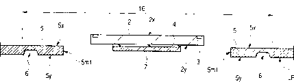
Accompanying drawing 1 is a width of cloth plan view (vertical view), shows the surface structure according to the semiconductor element of first embodiment of the invention.
Accompanying drawing 2 is width of cloth upward views (lower view) according to the semiconductor element of first embodiment of the invention.
Accompanying drawing 3 is the local amplification inclinating views in the accompanying drawing 2.
Accompanying drawing 4 (a) and 4 (b) show the internal structure of the semiconductor element of first embodiment, and wherein accompanying drawing 4 (a) is a plan view of removing resin sealing body top, and accompanying drawing 4 (b) is the viewgraph of cross-section that the straight line a-a in the accompanying drawing 4 (a) cuts open.
Accompanying drawing 5 is partial enlarged views of the viewgraph of cross-section in the accompanying drawing 4 (b).
Accompanying drawing 6 is a width of cloth end views, shows the part of surface structure of the semiconductor element of first embodiment.
Accompanying drawing 7 is perspective views that a width of cloth shows the lead-in wire rear surface in the accompanying drawing 5.
Accompanying drawing 8 is a width of cloth plan views, the part of the lead frame that the semiconductor element of demonstration manufacturing first embodiment is used.
Accompanying drawing 9 is that plan view is amplified in the part in the accompanying drawing 8.
Accompanying drawing 10 is viewgraph of cross-section that the straight line b-b in the accompanying drawing 9 cuts open.
Accompanying drawing 11 is a width of cloth upward views, shows and the relative rear surface, side shown in the accompanying drawing 9.
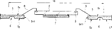
Accompanying drawing 12 (a) and 12 (b) show the manufacture process of the semiconductor element of first embodiment, and wherein accompanying drawing 12 (a) is the viewgraph of cross-section of display chip installation steps, and accompanying drawing 12 (b) is the viewgraph of cross-section that shows the lead engagement step.
Accompanying drawing 13 (a) and 13 (b) are presented at the resin-sealed step after the accompanying drawing 12 in the semiconductor element manufacture process, wherein accompanying drawing 13 (a) is the viewgraph of cross-section that is presented at lead frame positioning states in the mould, and accompanying drawing 13 (b) is the viewgraph of cross-section that shows resin-sealed state.
Accompanying drawing 14 is partial enlarged views of the viewgraph of cross-section in the accompanying drawing 13 (a).
Accompanying drawing 15 is a width of cloth viewgraph of cross-section, shows the plating step after the accompanying drawing 13 in the semiconductor element manufacture process.
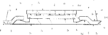
Accompanying drawing 17 is viewgraph of cross-section of the encapsulation state of the width of cloth semiconductor element that shows first embodiment.
Accompanying drawing 18 is partial enlarged views of the viewgraph of cross-section in the accompanying drawing 17.
Accompanying drawing 19 is a width of cloth viewgraph of cross-section, and demonstration is according to the part of the internal structure of the semiconductor element of second embodiment of the invention.
Accompanying drawing 20 is upward views (lower view) of lead-in wire shown in the accompanying drawing 19.
Accompanying drawing 21 is a width of cloth viewgraph of cross-section, and demonstration is according to the part of the internal structure of the semiconductor element of third embodiment of the invention.
Accompanying drawing 22 is upward views (lower view) of lead-in wire shown in the accompanying drawing 21.
Accompanying drawing 23 is a width of cloth viewgraph of cross-section, and demonstration is according to the part of the internal structure of the semiconductor element of fourth embodiment of the invention.
Accompanying drawing 24 is upward views (lower view) of lead-in wire shown in the accompanying drawing 23.
Accompanying drawing 25 is a width of cloth viewgraph of cross-section, and demonstration is according to the part of the internal structure of the semiconductor element of fifth embodiment of the invention.
Accompanying drawing 26 is upward views (lower view) of lead-in wire shown in the accompanying drawing 25.
Accompanying drawing 28 is viewgraph of cross-section that the straight line c-c in the accompanying drawing 27 cuts open.
Accompanying drawing 29 is a width of cloth viewgraph of cross-section, shows the internal structure according to the semiconductor element of seventh embodiment of the invention.
Accompanying drawing 30 (a) and 30 (b) show the internal structure according to the semiconductor element of eighth embodiment of the invention, wherein accompanying drawing 30 (a) is a plan view of removing resin sealing body top, and accompanying drawing 30 (b) is the viewgraph of cross-section that the straight line d-d along accompanying drawing 30 (a) cuts open.
Accompanying drawing 31 is partial enlarged views of the viewgraph of cross-section in the accompanying drawing 30 (b).
Accompanying drawing 32 is plan views of the used lead frame of the semiconductor element of manufacturing the 8th embodiment.
Accompanying drawing 33 is that the facing upward of part amplification in the accompanying drawing 32 attempted, and shows the rear surface as the apparent surface.
Accompanying drawing 34 (a) and 34 (b) show the manufacture process of the semiconductor element of the 8th embodiment, and wherein accompanying drawing 34 (a) is the viewgraph of cross-section that shows the lead engagement step, and accompanying drawing 34 (b) is the viewgraph of cross-section that shows resin-sealed step.
Accompanying drawing 35 (a) and 35 (b) show the semiconductor element manufacturing step after the accompanying drawing 34, and wherein accompanying drawing 35 (a) is the viewgraph of cross-section that shows plating step, and accompanying drawing 35 (b) is to show the viewgraph of cross-section of shearing step.
Accompanying drawing 36 is the plan views that show the resin sealing body that forms in the resin-sealed step shown in the accompanying drawing 35 (b).With
Accompanying drawing 37 is a width of cloth viewgraph of cross-section, shows the internal structure according to the semiconductor element of ninth embodiment of the invention.
Embodiment
Hereinafter with reference to accompanying drawing, describe embodiments of the invention in detail.At the institute's drawings attached that is used for illustrating embodiment, the part with identity function is used similar Reference numeral, and omits repeat specification.
(first embodiment)
In first embodiment, with the semiconductor element of QFN type as the lead-free semiconductor element, and, in this lead-free semiconductor element, come out to lead portion as being used for and the outside end portion that is connected in the rear surface of resin sealing body with its example of using as the present invention.
Accompanying drawing 1 to 18 is relevant with the semiconductor element according to first embodiment of the invention, wherein accompanying drawing 1 is the plan view (vertical view) that shows the surface structure of semiconductor element, accompanying drawing 2 is upward views (lower view) of semiconductor element, accompanying drawing 3 is partial enlarged views of the upward view (lower view) in the accompanying drawing 2, accompanying drawing 4 (a) and 4 (b) show the internal structure of semiconductor element, wherein accompanying drawing 4 (a) is a plan view of removing resin sealing body top, accompanying drawing 4 (b) is the viewgraph of cross-section that the straight line a-a in the accompanying drawing 4 (a) cuts open, accompanying drawing 5 is partial enlarged views of the viewgraph of cross-section in the accompanying drawing 4 (b), accompanying drawing 6 is the end views that show the part of semiconductor element surface structure, accompanying drawing 7 is the perspective views that show the rear surface of the lead-in wire in the accompanying drawing 5, accompanying drawing 8 is the plan views (vertical view) that show a part of making the used lead frame of semiconductor element, accompanying drawing 9 is partial enlarged views of the plan view in the accompanying drawing 8, accompanying drawing 10 is viewgraph of cross-section that the straight line b-b in the accompanying drawing 9 cuts open, accompanying drawing 11 is the upward views (lower view) that show the rear surface relative with the side shown in the accompanying drawing 9, accompanying drawing 12 (a) and 12 (b) show the manufacture process of semiconductor element, wherein accompanying drawing 12 (a) is the viewgraph of cross-section of display chip installation steps, accompanying drawing 12 (b) is the viewgraph of cross-section that shows the lead engagement step, accompanying drawing 13 (a) and 13 (b) show the resin-sealed step after the accompanying drawing 12, wherein accompanying drawing 13 (a) is the viewgraph of cross-section that is presented at lead frame positioning states in the mould, accompanying drawing 13 (b) is the viewgraph of cross-section that shows resin-sealed state, accompanying drawing 14 is partial enlarged views of the viewgraph of cross-section in the accompanying drawing 13 (a), accompanying drawing 15 is the viewgraph of cross-section that show accompanying drawing 13 plating step afterwards, accompanying drawing 16 is the viewgraph of cross-section that show accompanying drawing 15 shearing step afterwards, accompanying drawing 17 is the viewgraph of cross-section that show the encapsulation state of semiconductor element, and accompanying drawing 18 is partial enlarged views of the viewgraph of cross-section in the accompanying drawing 17.
In order to make accompanying drawing be more prone to see clearly, in the description of back, omit description in some accompanying drawing to coating.
Shown in accompanying drawing 4 (a) and 4 (b), the semiconductor element of this embodiment is represented with 1a, it has encapsulating structure, and this encapsulating structure has a semiconductor chip 2, a plurality of lead-in wire 5,7, four suspended lead 7a of chip strutting piece (die pad, joint), many closing lines 8 and a resin sealing body 9.Semiconductor chip 2, a plurality of lead-in wire 5, chip strutting piece 7, four suspended lead 7a and Duo Gen connecting line 8 are sealed by resin sealing body 9.
The flat shape of the semiconductor chip 2 that intersects with thickness direction is quadrangles, for example, is square in this embodiment.For example; semiconductor chip 2 comprises a semiconductor chip, be formed on multiple line layer that a plurality of transistor units, a plurality of insulating barriers on the semiconductor chip first type surface and line layer on the semiconductor chip first type surface constitute and layer of surface diaphragm (final diaphragm) covering multiple line layer, yet to this structure without limits.
On the first type surface 2x of semiconductor chip 2, form a plurality of junction points (electrode) 3.These junction points 3 are along the side arrangement of semiconductor chip 2.These junction points 3 are formed in the top line layer of multiple line layer of semiconductor chip 2 and by welding hole and come out, and this conjugate foramen is positioned at the surface protection film of semiconductor chip 2 and corresponding with junction point 3.
Shown in attached Fig. 1 and 2, the flat shape of the resin sealing body 9 that intersects with thickness direction is quadrangles, for example, is square in this embodiment.Resin sealing body 9 has first type surface (upper surface) 9x and a rear surface (lower surface, the package surface) 9y that is positioned at opposite side.The planar dimension of resin sealing body 9 (overall size) is bigger than the size of semiconductor chip 2.
In order to reduce pressure, for example, resin sealing body 9 is formed by the thermosetting resin of xenyl and phenols curing agent and silicon rubber, and adds filler therein.
The transfer molding method that employing is adapted to produce in batches is as a kind of method that forms resin sealing body 9.According to the transfer molding method, use the mould that has outer kettle, chute, resin inlet and die cavity, thermosetting resin injects in the chamber to form resin sealing body from shell by chute and resin inlet.
In making resin molded type semiconductor element process, adopt type transfer molding method or modular type transfer molding method one by one, this one by one type transfer molding method use and to have the lead frame that a plurality of products form zone (element-forming region), and be installed in the semiconductor chip that product forms the zone respectively and sealed one by one by resin; In modular type transfer molding method, be installed in product form the zone semiconductor chip be sealed jointly by resin.For example, type transfer molding method is adapted to make the semiconductor element 1a of this first embodiment one by one.
Shown in accompanying drawing 4 (a) and 4 (b), a plurality of lead-in wires 5 are arranged along the four side of resin sealing body 9, and extend to semiconductor chip 2 from the side 9z of resin sealing body 9.
A plurality of junction points 3 of semiconductor chip 2 are electrically connected to respectively on a plurality of lead-in wires 5.In first embodiment, the junction point 3 of semiconductor chip 2 and the energising that goes between between 5 connect by connecting line 8 realizations.An end of connecting line 8 is connected with the pad 3 of semiconductor chip 2, and its another relative end is connected with lead-in wire 5 in the position in semiconductor chip 2 outsides (on every side).For example, use gold (Au) line as connecting line 8.Adopt the nail head type of hot press and ultrasonic vibration to weld the example that (ball bonding connects) method is used as connecting line 8 methods of attachment.
As accompanying drawing 4 (a), shown in 4 (b) and the accompanying drawing 5, each lead-in wire 5 comprises that one is positioned at the first type surface 9x of resin sealing body 9 and the first surface 5x between the 9y of rear surface (relative with first type surface), one is positioned at a relative side with first surface 5x and comes out and the second surface 5y that do not covered by the resin of resin sealing body 9 from the rear surface 9y of resin sealing body 9, a first end face 5m1 who is positioned at semiconductor chip 2 sides, a second end face 5m2 who is positioned at the relative side of the first end face 5m1, with one from second surface 5y to the recessed sunk part 6 of first surface 5x side.
In first embodiment, first surface 5x is as the composition surface that is connected with connecting line 8.First surface 5x is to the inside and outside extension of resin sealing body 9, and outstanding from the side 9z of resin sealing body 9.Second surface 5y is as the outside end portion that connects.Second surface 5y comes out and stretches out from the side 9z of resin sealing body 9 from the rear surface 9y of resin sealing body 9.The first end face 5m1 links to each other with the first and second surperficial 5x, 5y.The second end face 5m2 is outstanding and link to each other with the first and second surperficial 5x, 5y from the side 9z of resin sealing body 9.
In first embodiment, to shown in the accompanying drawing 7, sunk part 6 stops at the second end face 5m2 place of lead-in wire 5 and comes out from the second end face 5m2 as accompanying drawing 5.Sunk part is separated from 5 two sides of going between, and these two sides are positioned at relative both sides along the Width of lead-in wire.Sunk part extends to the first end face 5m1 from the second end face 5m2.Further, shown in accompanying drawing 3 to 5, sunk part 6 is formed on the outside, side of resin sealing body 9.The inner wall surface of sunk part 6 links to each other with the second end face 5m2 with second surface 5y.
In making the lead frame process, the lead-in wire 5 that has sunk part 6 can be considered to form by etch step when forming predetermined lead-in wire figure.
Shown in accompanying drawing 5 and 6, comprise that the surface of lead-in wire 5 of the inner wall surface of second surface 5y and sunk part 6 is covered by coating 10, the welding material wettability of this coating is than the wettability height of lead-in wire 5 when being welded to semiconductor element 1a on the distribution substrate.So form coating 10 so that cover the whole inner wall surface of whole second surface 5y, sunk part 6 of lead-in wire and the whole unsealing part (being positioned at the part in the outside, resin sealing body 9 sides) of 5 the first surface 5x of going between.
Such as will be described, the second end face 5m2 of lead-in wire 5 forms by cut off lead-in wire 5 from the chassis body of lead frame in shearing step, and described shearing step is included in the manufacture process of semiconductor element 1a.On the other hand, before the shearing step of lead-in wire 5, in the plating step, form coating 10.Therefore, the second end face 5m2 of lead-in wire 5 is not covered by coating 10 basically.In this first embodiment, yet except that the coating 10 of the second surface 5y that covers lead-in wire 5, a coating 10 that covers the inner wall surface of sunk part 6 comes out in the termination of the second end face 5m2 place and from second end face.
Owing to form the purpose of coating 10 is in order to guarantee the wettability of scolder when being welded to semiconductor element 1a on the distribution substrate, therefore selecting the suitable material of coating according to the used welding material of encapsulation.Preferably use and the material of the material that encapsulates used welding material identical component as coating 10.For example, in first embodiment, in order to mate the lead-free solder that (the tin)-Bi (bismuth) that has Sn forms, it is used for encapsulation, uses the coating of same composition, for example, and Sn-Bi.For example this Sn-Bi electrodeposited coating can easily form by electrolytic plating method, and electrolytic plating method is suitable for producing in batches.
As accompanying drawing 4 (b) with shown in 5, chip substrate 7 is littler than the overall size of semiconductor chip 2, and its thickness is than first and second surperficial 5x of lead-in wire 5 and the thin thickness between the 5y.Chip strutting piece 7 has a first type surface and rear surface that is oppositely arranged.The rear surface 2y of semiconductor chip 2 contacts with the first type surface of chip strutting piece 7 by adhesive 4.The rear surface of chip strutting piece 7 is covered by the resin of resin sealing body 9.
Shown in accompanying drawing 2 and 3, four suspended lead 7a extend from four angle chip strutting pieces 7 of resin sealing body 9.Each suspended lead 7a comprises first's (chip strutting piece 7 sides) and second portion (the turning side of resin sealing body 9), first and chip strutting piece 7 form one and extend to the turning of resin sealing body 9 from chip strutting piece 7, and second portion and first form one and extend to the turning of resin sealing body 9 from first.First has identical thickness with chip strutting piece 7 in fact and is positioned at the inside of resin sealing body 9.Second portion in fact with lead-in wire 5 first and second surfaces between part have identical thickness, and come out from the rear surface 9y of resin sealing body 9 in itself and the second surface 5y surface that is positioned at same side.
In the semiconductor element 1a of first embodiment, resin part (outstanding resin part) 9a and resin sealing body 9 form one, and the position between adjacent legs 5 is outstanding from each side 9z of resin sealing body.When forming resin sealing body 9 according to the transfer molding method, resin is from the space of die cavity inflow between the adjacent lead-in wire of mould mating surface of mould, thus formation resin part 9a.In first embodiment, resin part 9a can be retained, and also can be removed in manufacture process.
With reference to the accompanying drawings 8 to 11, make the used lead frame of semiconductor element 1a with describing.
As shown in Figure 8, represent lead frame with LF, it has a multiple frame structure, the a plurality of products that formed by chassis body (support) 15 divisions in this multiple frame structure inside form zone (element-forming region) 16 and are arranged in matrix shape, and described chassis body 15 comprises an outside framework part and an inner frame part.A plurality of lead-in wires 5, chip strutting piece 7 and four suspended lead 7a are arranged in each product and form regional 16 inside, shown in accompanying drawing 9 to 11.A plurality of lead-in wire 5 spaced apart become four lead wire set.Lead-in wire 5 in each lead wire set forms one with chassis body 15.Chip strutting piece 7 forms one by four suspended lead 7a and chassis body 15.
Each all has first surface 5x, second surface 5y, the first end face 5m1 and sunk part 6 in the lead-in wire 5.In accompanying drawing 9 to 11, the shear line of lead-in wire 5 is sheared in numeral 18 expressions from chassis body 15.Numeral 19 expressions are used for resin-sealed mold pressing line (potted line).Shear line 18 is between chassis body 15 and mold pressing line 19.In accompanying drawing 11, sunk part 6 usefulness hacures are represented.
After shearing, form sunk part 6, the i.e. position of shear line 18 in the position of coming out from 5 the shear surface of going between.In first embodiment, form sunk part 6, make it across (crossing) shear line 18.In the lead-in wire shown in the accompanying drawing 55, the second end face 5m2 is by shearing the shear surface that lead-in wire obtains along the shear line shown in the accompanying drawing 5 18.Therefore, each lead-in wire 5 that sunk part 6 comes out from the second end face 5m2, can be as first embodiment, by forming sunk part 6 so that it is formed across shear line 18, also can be by forming sunk part 6 so as to make its partly with shear line 18 overlapping formation.
First's (not shown) of chip strutting piece 7 and each suspended lead 7a is than the first surface 5x of each lead-in wire 5 and the thin thickness of the part between the second surface 5y.When can forming the predetermined leads figure in making lead frame LF, the first of chip strutting piece 7, suspended lead 7a and sunk part 6 consider to form by etching step.
So the lead frame LF that forms of structure forms predetermined lead-in wire graphic making by etching or compacting or etching and pressed metal sheet to form, and for example, sheet metal is formed by Cu (copper), Cu alloy or Fe (iron)-Ni (nickel) alloy.
Next, the manufacture process of semiconductor element 1a is described with reference to accompanying drawing 12 to 16.
At first, not only provide the lead frame LF shown in the accompanying drawing 8 to 11, and the semiconductor chip 2 shown in the accompanying drawing 4 is provided.
Then, shown in accompanying drawing 12 (a), each product that semiconductor chip 2 is installed in lead frame LF forms in the zone 16.The installation of semiconductor chip 2 is the rear surface 2y of semiconductor chip 2 to be engaged and is fixed on the first type surface of chip strutting piece 7 by adhesive 4 to finish.
Then, in each product of lead frame LF formed zone 16, a plurality of pads 3 on the semiconductor chip 2 and a plurality of lead-in wire 5 were electrically connected mutually by many connecting lines 8, shown in accompanying drawing 12 (b).The connection of connecting line 8 is that the nail head type welding by the anode solder type carries out, and in this welding, the pad 3 on the semiconductor chip 2 is the main sides that connect, and the first surface 5x of lead-in wire 5 time connects side.
Then, shown in accompanying drawing 13 (a), lead frame LF is between the patrix 20a and counterdie 20b of mould 20.The location of lead frame LF is to finish under the state between the mating surface of sheet material 22 insertion rear surfaces (and second surface 5y homonymy of lead-in wire 5) and counterdie 20b.For example, when using sheet material 22, resin sheet can bear the mold pressing heating-up temperature and can be rolled by the clamping pressure of mould (compression stress).
Being positioned under the following state of lead frame LF finished, and promptly semiconductor chip 2, lead-in wire 5, chip strutting piece 7, suspended lead 7a and connecting line 8 each product of being positioned at lead frame LF forms the state of each 21 inside, chamber in zone 16.
Being positioned under the following state of lead frame LF finished, promptly extend to the mating surface of chamber 21 and patrix 20a, and the state of 5 the unsealing part location lead-in wire 5 between the mating surface of upper die and lower die 20a, 20b the time that goes between.
Mating surface by upper die and lower die 20a, 20b clamps unsealing part and the sheet material 22 and the corresponding part of lead-in wire unsealing part of (press and press) lead-in wire 5, locatees lead frame LF.
Being positioned under the impaction state of lead frame LF finished, and bears the clamping pressure (compression stress) between upper die and lower die 20a, the 20b so that go between 5 sheet materials 22 of nipping at sheet material 22 under this state.
Further, being positioned under the following state of lead frame LF finished, and the sunk part 6 of lead-in wire 5 is positioned at the outside (outside of mold pressing line 19) in chamber 21 under this state, promptly between the mating surface of upper die and lower die 20a, 20b.
Then, locate lead frame LF like this after, mold pressing resin, thermosetting epoxy resin for example injects chamber 21 to form resin sealing body 9, shown in accompanying drawing 13 (b) by the relevant portion that selects, chute, resin inlet from the shell of mould 20.Semiconductor chip 2, lead-in wire 5, chip strutting piece 7, suspended lead 7a and connecting line 8 are sealed by resin sealing body 9, and 5 the second surface 5y of going between comes out from the rear surface 9y of resin sealing body 9.
In this step, sunk part 6 with separate along two relative sides of the Width of associated lead 5.In addition, because the second surface 5y of lead-in wire 5 is oppressed by thin plate 22 once more, enter the unfavorable of sunk part 6 so can get rid of resin.
Then, the sheet material 22 that is attached to lead frame LF rear surface is peeled off and lead frame LF is taken out from mould 20, then is the curing schedule that improves the hardness of resin sealing body 9.Then, as shown in Figure 15, on the surface of the lead frame LF of the inner wall surface that comprises lead-in wire 5 second surface 5y and sunk part 6, form coating 10.For example, form coating 10 by the electrolytic plating method that is adapted to produce in batches.
Then, lead frame LF enters a shear, and lead-in wire 5 is sheared along shear line 18 (seeing accompanying drawing 11) in the following manner.As shown in Figure 16, the unsealing part of lead-in wire (part of giving prominence to from the side of resin sealing body 9) is punched the punch guider 26 of mould 25 and receives substrate 27 vertical maintenances with chassis body 15, cutting punch 28 receives substrate 27 liftings from punch guider 26 1 side direction then, and lead-in wire 5 is sheared the shearing motions of drift 28 and reception substrate 27 and shears.
In this shears step, because be to form, so sunk part 6 comes out from shear surface (the second end face 5m2) after shearing in the position (shear line 18) of coming out from 5 the shear surface of going between.In addition, because the inner wall surface of sunk part 6 is covered by coating 10, except the coating 10 that forms on the second surface 5y of lead-in wire 5, the coating 10 that forms on the inner wall surface of sunk part 6 comes out from shear surface (the second end face 5m2).Now, the semiconductor element 1a shown in the accompanying drawing 1 to 6 finishes substantially.
The method of shearing lead-in wire 5 is not limited to cutting punch 28 and receives the method that substrate 27 promotes from punch guider 26 1 side direction.Can adopt cutting punch 28 from receiving the method that substrate 27 1 side direction punch guiders 26 reduce.Further, also can adopt the cutting method that uses cutting edge.
17 and 18 encapsulation of describing semiconductor element 1a with reference to the accompanying drawings.
Shown in accompanying drawing 17 and 18, semiconductor element 1a is welded on the distribution substrate 30.For example, finish welding by the Reflow Soldering connection.More particularly, for example, at first adopt screen printing scolder 32 like the paste to be placed on the electronic pads (lug plate, leg) 31 on the package surface of distribution substrate 30.Then, semiconductor element 1a locatees by this way,, is used for the electronic pads 31 that the outside end portion that connects of semiconductor element (the second surface 5y of lead-in wire 5) is positioned at distribution substrate 30 that is.Then, semiconductor element 1a is installed on the package surface of distribution substrate 30, then distribution substrate 30 is placed in for example infrared ray reflow ovens, and after this, solder fusing is solidifying.As a result, the lead-in wire 5 of semiconductor element 1a is fixed, and mechanically is electrically connected to by scolder 32 on the electronic pads 31 of distribution substrate 30.
Under the situation of conventional wire, on second end face (from the outstanding end face of resin-sealed body side surface) of lead-in wire, do not form coating, on second end face of lead-in wire so when being welded to semiconductor element on the distribution substrate, scolder can not melt.On the other hand, as shown in Figure 5, respectively going between of using in first embodiment 5 has sunk part 6, this sunk part is recessed and link to each other with the second end face 5m2 to first surface 5x from second surface 5y, and the coating 10 that is formed on the inner wall surface of sunk part 6 comes out from the second end face 5m2.Therefore, shown in accompanying drawing 17 and 18, scolder 32 soaks on the second end face 5m2 of lead-in wire 5 and form leg on the second end face 5m2.Because scolder 32 soaks on the second end face 5m2 of lead-in wire 5, the bonding area between lead-in wire 5 and the scolder 32 increases, thereby the weld strength between the lead-in wire 5 of the electronic pads 31 of distribution substrate 30 and semiconductor element 1a improves.Like this, just can improve the package reliability of semiconductor element 1a.
In addition, bonding area between lead-in wire 5 and the scolder 32 is increased to the degree suitable with the degree of depth of sunk part 6, weld strength between the electronic pads 31 of distribution substrate 30 and the lead-in wire 5 of semiconductor element 1a increases, so the package reliability of semiconductor element 1a can further improve.
QFN N-type semiconductor N component size (planar dimension) dwindle can be by shortening semiconductor chip each side and the distance between each side 9z of resin sealing body 9 realize.Yet, in order to reduce the distance, be necessary to shorten each lead-in wire 5, thereby the length of 5 the second surface of going between (being used for the outside end portion that connects) 5y shortens.Because the length of the second surface 5y of lead-in wire 5 shortens, the electronic pads 31 of distribution substrate 30 and the bonding area that goes between between 5 diminish during the welding semiconductor element, so the encapsulation defective that comes off from distribution substrate 30 such as semiconductor element 1a is more prone to occur.
In first embodiment, as previously described, because scolder 32 soaks on the second end face 5m2 of lead-in wire 5, the bonding area between lead-in wire 5 and the scolder 32 increases.In addition, the bonding area between lead-in wire 5 and the scolder 32 is increased to and the suitable degree of the degree of depth of the sunk part 6 that goes between.Therefore, even the size of semiconductor element 1a is dwindled the contraction in length of 5 the second surface 5y of causing going between, also can contain the generation of the encapsulation defective that comes off from distribution substrate 30 such as semiconductor element 1a.Can guarantee package reliability when just, semiconductor element 1a size is dwindled.
According to inventor's of the present invention research,, also can increase the bonding area between lead-in wire 5 and the scolder 32 even form sunk part at the cutting out section (shear line 18) of lead-in wire; Described sunk part from 5 the second surface 5y of going between to first surface 5x recessed and with link to each other along two relative sides of the Width of lead-in wire.Yet, having under the situation of this sunk part, the resin that enters between the adjacent legs in the mold pressing step enters sunk part, and sunk part covered by resin, so be necessary to remove resin before forming coating 10.This causes manufacturing cost to increase.On the other hand, because employed sunk part 6 is separated with two sides of each lead-in wire 5 among first embodiment, so the resin that enters between the adjacent legs can not enter sunk part 6.
Further, even form the first and second surperficial 5x that extend through lead-in wire 5, the through hole of 5y at the cutting out section of lead-in wire 5, the bonding area between lead-in wire 5 and the scolder 32 also can increase.Have under the situation of this through hole, the resin that enters between the adjacent legs can not enter through hole, but because the first surface 5x of the mating surface of the patrix 20a of mould 20 and each lead-in wire is lower in bonding, very small amount of resin can enter between the two and enter through hole.This is not the formation of restriction through hole, but the situation of formation sunk part also is a necessary being in the first surface 5x of lead-in wire 5.If resin enters from 5 the first surface 5x of going between, then sunk part is covered by resin, just is necessary to remove resin before forming coating 10, and this causes the manufacturing cost increase.If the clamping pressure of mould 20 increases to the degree that causes 5 strains that respectively go between, just can stop resin to enter the mating surface of patrix 20a and 5 the first surface 5x of going between between, but can cause output to reduce.In addition, because this through hole, thereby the intensity of the volume-diminished of lead-in wire 5 lead-in wire reduces, so easier appearance encapsulation defective.On the other hand, sunk part used among first embodiment does not link to each other with the first surface 5x of lead-in wire 5, therefore there is no need the clamping pressure of mould 20 is increased to the degree that causes lead-in wire 5 strains.Further, between the mating surface of each lead-in wire 5 second surface 5y and counterdie 20b, be provided with sheet material 22, lead-in wire 5 second surface 5y and the bonding force between the sheet material 22 are bigger than the bonding force between the mating surface of counterdie 20b and 5 the second surface 5y of going between, thus resin can not enter thin plate 22 and 5 the second surface 5y of going between between.
Like this, according to first embodiment, can improve the package reliability of semiconductor element 1a.In addition, the size that can dwindle semiconductor element 1a is guaranteed package reliability simultaneously.In addition, the semiconductor element 1a that package reliability is very high can produce in a large number.Further, can produce the very high semiconductor element 1a of package reliability at low cost.
(second embodiment)
In a second embodiment, the example of the semiconductor element of the lead-in wire that has an anti-drop device of the present invention will describe be used.
Accompanying drawing 19 is a width of cloth viewgraph of cross-section, and demonstration is according to the part of the internal structure of the semiconductor element of second embodiment of the invention, and accompanying drawing 20 is upward views (lower view) of lead-in wire shown in the accompanying drawing 19.
As shown in Figure 19, the semiconductor element of second embodiment represents that with 1b it has identical construction with aforementioned first embodiment basically, and difference is the structure of each lead-in wire 5.
Shown in accompanying drawing 19 and 20, except top structure, each lead-in wire 5 has the 3rd a surperficial 5y1 who is positioned at a relative side with first surface 5x, and the 3rd surface ratio second surface 5y is more near first surface 5x.The 3rd surperficial 5y1 links to each other with the first end face 5m1, is positioned at resin sealing body 9 inside, and resin-sealed by resin sealing body 9.The 3rd surperficial 5y1 is set is in order to stop lead-in wire 5 to come off from resin sealing body 9.
When having the 3rd surperficial 5y1 to come off in each lead-in wire 5 to stop lead-in wire, the contraction in length of the second surface of lead-in wire 5, when being welded to semiconductor element 1b on the distribution substrate 30, bonding area between lead-in wire 5 and the scolder 32 dwindles, thereby the weld strength between the lead-in wire 5 of the electronic pads 31 of distribution substrate 30 and semiconductor element 1 reduces.Yet, because the dwindling of bonding area that each lead-in wire 5 existence that have sunk part 6, the three surperficial 5y1 causes limited.Like this, the present invention is effectively applied to comprise the semiconductor element of the lead-in wire 5 with anti-drop device.
By when making lead frame, considering to adopt etching step can form the 3rd surperficial 5y1 at an easy rate.After lead-in wire forms, also can form the 3rd surface at an easy rate by bending lead.In this case, first surface 5x comprises the part of differing heights, and particularly, lead connects first on it and the second portion lower than first.
(the 3rd embodiment)
In the 3rd embodiment, first modification will be described, in this modification, change the shape of the sunk part in each lead-in wire.
Accompanying drawing 21 is a width of cloth viewgraph of cross-section, and demonstration is according to the part of the internal structure of the semiconductor element of third embodiment of the invention, and accompanying drawing 22 is upward views (lower view) of lead-in wire shown in the accompanying drawing 21.
Sunk part 6 is formed at the outside of the side 9z of resin sealing body 9 in first embodiment.As shown in Figure 21, sunk part 6 is formed at the outside and the inboard of the side 9z of resin sealing body 9 in the 3rd embodiment.As shown in Figure 22, sunk part 6 comes out from each lead-in wire second end face 5m2 of 5, and with separate and also separate along two relative sides of the Width of lead-in wire 5 with the first end face 5m1.According to this structure, compare with first embodiment, the semiconductor element of this embodiment is represented with 1c, install by welding, bonding area between each lead-in wire 5 and the scolder 32 increases, weld strength between the electronic pads 31 of distribution substrate 30 and the lead-in wire 5 of semiconductor element 1c also increases, and therefore can improve the package reliability of semiconductor element 1c.
(the 4th embodiment)
In the 4th embodiment, a modification will be described, in this modification, change the shape of the sunk part in each lead-in wire.
Accompanying drawing 23 is a width of cloth viewgraph of cross-section, and demonstration is according to the part of the internal structure of the semiconductor element of fourth embodiment of the invention.Accompanying drawing 24 is upward views (lower view) of lead-in wire shown in the accompanying drawing 23.
Although the sunk part of describing among first and second embodiment 6 is close with the second end face 5m2 of each lead-in wire 5, among the 4th embodiment used sunk part 6 with separate along two relative sides of the Width of lead-in wire, and also separate with the first and second end face 5m1,5m2.Among the 4th embodiment used sunk part 6 be provided with a plurality of so that intersperse among the outside and the inboard of the side 9z of resin sealing body 9.According to this structure, the semiconductor element of this embodiment is represented with 1d, in the time of on being soldered to distribution substrate 30, bonding area between lead-in wire 5 and the scolder 32 increases, thereby the weld strength between the lead-in wire 5 of the electronic pads 31 of distribution substrate 30 and semiconductor element 1d increases, so also can improve the package reliability of semiconductor element 1d in this embodiment.In addition, the size that can dwindle semiconductor element 1d is also guaranteed package reliability simultaneously.
(the 5th embodiment)
In the 5th embodiment, a modification will be described, in this modification, change the shape of the sunk part in each lead-in wire.
Accompanying drawing 25 is a width of cloth viewgraph of cross-section, and demonstration is according to the major part of the internal structure of the semiconductor element of fifth embodiment of the invention.Accompanying drawing 26 is upward views (lower view) of lead-in wire shown in the accompanying drawing 25.
Each used among the 5th embodiment lead-in wire 5 includes a first surface 5x, second surface 5y, first an end face 5m1, the second end face 5m2 and an a plurality of sunk part 6; Described first surface is between the first type surface 9x and rear surface 9y of resin sealing body 9, described second surface is positioned at a side relative with first surface 5x, and come out from the rear surface 9y of resin sealing body 9, described first end face is positioned at semiconductor chip 2 one sides, the described second end face 5m2 is positioned at a side relative with the first end face 5m1, and come out from the side 9z of resin sealing body 9, described sunk part is recessed to first surface 5x from second surface 5y.Have at least second an end face 5m2 with lead-in wire 5 to link to each other in a plurality of sunk parts 6, the inner wall surface of second surface 5y and a plurality of sunk part 6 is covered by coating 10, and this coating has higher solder wettability than the second end face 5m2 of lead-in wire 5.A plurality of sunk parts 6 are dispersed in the outside and the inboard of the side 9z of resin sealing body 9.
In the 5th embodiment, the semiconductor element with lead-in wire 5 of this structure is represented with 1e, can obtain the effect identical with first embodiment.
(the 6th embodiment)
In the 6th embodiment, an example is described, the present invention is applied to have the semiconductor element of the chip strutting piece that comes out from the resin sealing body rear surface in this example.
Accompanying drawing 27 is a width of cloth upward views (lower view), shows the surface structure according to the semiconductor element of sixth embodiment of the invention, and accompanying drawing 28 is viewgraph of cross-section of the major part cut open of the straight line c-c in the accompanying drawing 27.
The semiconductor element of the 6th embodiment is represented with 1f, shown in accompanying drawing 27 and 28, it has encapsulating structure, in this encapsulating structure, the rear surface 2y of semiconductor chip 2 joins on first type surface (chip installed surface) 7x of chip strutting piece 7 by adhesive 4, and the rear surface 7y of the chip strutting piece 7 relative with first type surface 7x comes out from the rear surface 9y of resin sealing body 9.Chip strutting piece 7 have one from rear surface 7y to the recessed sunk part 35 of first type surface 7x.Sunk part 35 is separated with the peripheral edge of chip pad 7, and not approaching with the side of chip strutting piece 7.Although do not show that the inner wall surface of sunk part 35 is covered by coating 10 as previously described sunk part 6.
By in chip strutting piece 7, forming such sunk part 35, bonding area when being welded to semiconductor element 1f on the distribution substrate between chip strutting piece and the welding material increases, thereby the package reliability that chip strutting piece 7 is welded on the semiconductor element 1f improves.
(the 7th embodiment)
In the 7th embodiment, an example will be described, the present invention's QFN semiconductor element of structure that is applied to face down in this example.
Accompanying drawing 29 is a width of cloth viewgraph of cross-section, and demonstration is according to the major part of the internal structure of the semiconductor element of seventh embodiment of the invention.
As shown in Figure 29, the semiconductor element of the 7th embodiment is represented with 1g, the device that it adopts projected electrode 36 to be electrically connected mutually as pad 3 and lead-in wire 5 with semiconductor chip 2.Each projected electrode 36 is between the pad 3 of semiconductor chip 2 and 5 the first surface 5x of going between, so that with their mechanical connections and be electrically connected.In the semiconductor element 1g of this structure that faces down, can obtain the effect identical with first embodiment.
(the 8th embodiment)
In first embodiment, provided the foundation example of type transfer molding manufactured semiconductor element one by one, and in the 8th embodiment, will provide example according to modular type transfer molding manufactured semiconductor element.
Accompanying drawing 30 (a) and 30 (b) show the internal structure according to the semiconductor element of eighth embodiment of the invention, wherein accompanying drawing 30 (a) is a plan view of removing resin sealing body top, and accompanying drawing 30 (b) is the viewgraph of cross-section that the straight line d-d along accompanying drawing 30 (a) cuts open; Accompanying drawing 31 is partial enlarged views of the viewgraph of cross-section in the accompanying drawing 30 (b); Accompanying drawing 32 is plan views of the used lead frame of the semiconductor element of manufacturing the 8th embodiment; Accompanying drawing 33 is upward views of the local accompanying drawing 32 that amplifies, shows the rear surface as the apparent surface; Accompanying drawing 34 (a) and 34 (b) show the manufacture process of the semiconductor element of the 8th embodiment, and wherein accompanying drawing 34 (a) is the viewgraph of cross-section that shows the lead Connection Step, and accompanying drawing 34 (b) is the viewgraph of cross-section that shows resin-sealed step; Accompanying drawing 35 (a) and 35 (b) show the manufacture process of the semiconductor element after the accompanying drawing 34, and wherein accompanying drawing 35 (a) is the viewgraph of cross-section that shows the plating step, and accompanying drawing 35 (b) is to show the viewgraph of cross-section of shearing step; Accompanying drawing 36 is the plan views that show the resin sealing body that forms in the resin-sealed step shown in the accompanying drawing 35 (b).
Shown in accompanying drawing 30 and 31, the semiconductor element 1h of the 8th embodiment has identical construction with first embodiment basically, and difference is following structure.
In the used resin sealing body 9 of the 8th embodiment, first type surface 9x almost has identical overall dimension with rear surface 9y, and side 9z is vertical with rear surface 9y with first type surface 9x in fact.Further, the second end face 5m2 of lead-in wire 5 is concordant with the side 9z of resin sealing body 9 in fact.
In order to make the semiconductor element 1h of the 8th embodiment, adopt modular type transfer molding method, this modular type transfer molding method is used has the lead frame LF1 (seeing accompanying drawing 32 and 33) that a plurality of products form the zone, and is installed in product respectively forms the semiconductor chip in zone 16 by the resin integral sealing in this die pressing.According to modular type transfer molding method, after resin sealing body formed, lead frame and resin sealing body were divided into single product and form zone (being divided into single fritter).
33 to 35 manufacturings of describing semiconductor element 1h below with reference to accompanying drawings.
At first, provide the LF1 of the lead frame shown in accompanying drawing 32 and 33, each product at lead frame LF1 forms in the zone 16 then, semiconductor chip 2 is engaged and is fixed on the chip strutting piece 7, shown in accompanying drawing 34 (a).Afterwards, in each product forms zone 16, be electrically connected by a plurality of pads 3 and a plurality of lead-in wire 5 of many connecting lines 8, shown in accompanying drawing 34 (a) semiconductor chip 2.
Then, the product that is arranged in lead frame LF1 forms semiconductor chip 2 in the zone 16 by the resin integral sealing, and as accompanying drawing 34 (b) with shown in 35, a plurality of products form zone 16 and sealed by single resin sealing body 9.In each product formed zone 16, the second surface 5y of lead-in wire 5 came out from the rear surface 9y of resin sealing body 9.
Then, shown in accompanying drawing 35 (a), form the zone at each product, the second surface 5y and the sunk part 6 of lead-in wire 5 are covered by coating 10.For example, form coating 10 by electrolytic plating method.
Then, shown in accompanying drawing 35 (b), lead frame LF and resin sealing body 9 are cut into single resin sealing body 9, for example adopt shearing knife edge 37 to shear along shear line 18.The semiconductor chip 1h of the 8th embodiment shown in the accompanying drawing 30 and 31 just makes and finishes like this.
Like this, in the 8th embodiment, also can obtain the effect identical with first embodiment.
(the 9th embodiment)
In the 9th embodiment, the example that the present invention is applied to QON (profile is tetragonal Lead-free in Electronic Packaging) will be described, be exposed to the first type surface 9x of resin sealing body 9 at QON chips strutting piece 7.
Accompanying drawing 37 is a width of cloth viewgraph of cross-section, shows the internal structure according to the semiconductor element of ninth embodiment of the invention.
Semiconductor element is represented with 1j in the 9th embodiment, and as shown in Figure 37, semiconductor chip 2 is installed on the chip strutting piece 7 in the mode that the first type surface 2x of chip is exposed to the rear surface 9y of resin sealing body 9.Chip strutting piece 7 is exposed to the first type surface 9x of resin sealing body 9.Chip strutting piece 7 is bigger than the area of the first type surface 2x of semiconductor chip 2, therefore can improve heat dispersion.The pad 3 of semiconductor chip 2 and go between between 5 connects by connecting line 8 energisings.A terminal pad 3 that connects semiconductor chip 2 of connecting line 8, and the opposite end of connecting line is connected and fixed the rear surface (the 3rd surperficial 5y2) of lead-in wire 5 in position, the outside of semiconductor chip (on every side).In the semiconductor element 1j of QON type, can obtain the effect identical with first embodiment.
Although bigger than the area of the first type surface 2x of semiconductor chip 2 at the 9th embodiment chips strutting piece 7, this structure is not restrictive.Chip strutting piece 7 also can be littler than the area of the first type surface 2x of semiconductor chip 2.
Although on the basis of superincumbent embodiment the present invention is specifically described, the present invention is not limited to top embodiment certainly, under the situation that does not break away from essence of the present invention multiple variation can be arranged.
For example, apply the present invention to a kind of lead-free semiconductor element SON (small-sized Lead-free in Electronic Packaging).
Claims (26)
1. semiconductor element comprises:
One block semiconductor chip, this semiconductor chip have first type surface and the rear surface that is positioned at opposite side, and further have a plurality of electrodes that are arranged on the first type surface;
A plurality of lead-in wires, they respectively be formed at semiconductor chip on a plurality of electrodes be electrically connected; With
A resin sealing body is used for sealing semiconductor chips and a plurality of lead-in wire;
Wherein, each lead-in wire all has a first surface, a second surface, first end face, second end face and a sunk part; Described first surface is between the rear surface of the first type surface of resin sealing body and the resin sealing body relative with first type surface, described second surface is positioned at a side relative with first surface and comes out from the rear surface of resin sealing body, described first end face is positioned at semiconductor chip side, described second end face is positioned at a side relative with first end face and comes out from the side of resin sealing body, described sunk part is recessed and link to each other with second end face to the first surface side from second surface, and
Wherein, the inner wall surface of second surface and sunk part is covered by coating, and described coating has higher solder wettability than second end face of each lead-in wire.
2. semiconductor element as claimed in claim 1 is characterized in that
Sunk part stops in second end of each lead-in wire and comes out from second end face.
3. semiconductor element as claimed in claim 1 is characterized in that
Coating stops in second end of each lead-in wire and comes out from second end face.
4. semiconductor element as claimed in claim 1 is characterized in that
Separate two sides of sunk part and each lead-in wire, and described side is positioned at opposite side along the Width of lead-in wire.
5. semiconductor element as claimed in claim 1 is characterized in that
Each second end face of each lead-in wire is a shear surface.
6. semiconductor element as claimed in claim 1 is characterized in that
First and second surfaces of each lead-in wire link to each other with second end face, and
Wherein, second end face is outstanding from the side of resin sealing body.
7. semiconductor element as claimed in claim 6 is characterized in that
The sunk part of each lead is formed at the outside of resin sealing body.
8. semiconductor element as claimed in claim 1 is characterized in that
The sunk part of each lead-in wire is formed at the outside and the inboard of a side of resin sealing body.
9. semiconductor element as claimed in claim 1 further comprises many connecting lines, is used for a plurality of electrodes of semiconductor chip are electrically connected with the first surface of a plurality of lead-in wires.
10. semiconductor element as claimed in claim 9 further comprises the chip strutting piece that a thickness is thinner than lead-in wire,
Wherein, the rear surface of semiconductor chip engages with the first surface of chip strutting piece,
The second surface that is positioned at the chip strutting piece of a relative side with first surface is covered by the resin of resin sealing body.
11. semiconductor element as claimed in claim 1 further comprises a chip strutting piece,
This chip strutting piece has a first surface, a second surface and a sunk part, described first surface engages with semiconductor chip, described second surface is positioned at a side relative with first surface and comes out from the rear surface of resin sealing body, and described sunk part is recessed and come out from the rear surface of resin sealing body to the first surface side from second surface.
12. semiconductor element as claimed in claim 1 is characterized in that
A plurality of electrodes of semiconductor chip are electrically connected with the first surface of a plurality of lead-in wires respectively by projected electrode.
13. a semiconductor element, it comprises:
One block semiconductor chip, this semiconductor chip have first type surface and the rear surface that is positioned at opposite side, and further have a plurality of electrodes that are arranged on the first type surface;
A plurality of lead-in wires, they respectively be formed at semiconductor chip on a plurality of electrodes be electrically connected; With
A resin sealing body is used for sealing semiconductor chips and a plurality of lead-in wire;
Wherein, each lead-in wire all has a first surface, this first surface between the rear surface of the first type surface of resin sealing body and the resin sealing body relative with first type surface,
A second surface, this second surface be positioned at a side relative with first surface and come out from the rear surface of resin sealing body and
A sunk part, this sunk part is recessed to the first surface side from second surface, and
Wherein, the inner wall surface of second surface and sunk part is covered by coating, and described coating has higher solder wettability than second end face of each lead-in wire.
14. semiconductor element as claimed in claim 13 is characterized in that
Each lead-in wire has a plurality of sunk parts.
15. a semiconductor element comprises:
One block semiconductor chip, this semiconductor chip have first type surface and the rear surface that is positioned at opposite side, and further have a plurality of electrodes that are arranged on the first type surface;
A plurality of lead-in wires, they respectively be formed at semiconductor chip on a plurality of electrodes be electrically connected; With
A resin sealing body is used for sealing semiconductor chips and a plurality of lead-in wire;
Wherein, each lead-in wire all has a first surface, this first surface between the rear surface of the first type surface of resin sealing body and the resin sealing body relative with first type surface,
A second surface, this second surface are positioned at a side relative with first surface and come out from the rear surface of resin sealing body,
First end face that is positioned at semiconductor chip side,
One be positioned at a side relative and second end face that comes out from the side of resin sealing body with first end face and
A plurality of from second surface to the recessed sunk part of first surface side,
Wherein, at least one of a plurality of sunk parts links to each other with second end face of each lead-in wire, and
The inner wall surface of second surface and each sunk part is covered by coating, and described coating has higher solder wettability than second end face of each lead-in wire.
16. semiconductor element as claimed in claim 15 is characterized in that
First and second surfaces link to each other with second end face,
Second end face is outstanding from the side of resin sealing body, and
A plurality of sunk parts intersperse among the outside and the inboard of resin-sealed body side surface.
17. the manufacture method of a semiconductor element comprises the steps:
The lead frame that comprises semiconductor chip and lead-in wire is provided, this semiconductor chip and lead-in wire are sealed by resin sealing body, each lead-in wire has a first surface, a second surface and a sunk part, described first surface extends the inboard and outside and outstanding from the side of resin sealing body of resin sealing body, described second surface is positioned at a side relative with first surface and comes out from the rear surface of resin sealing body, and extend the outside of resin-sealed body side surface, described sunk part is recessed to the first surface side from second surface;
Form coating on the inner wall surface of the second surface of each lead-in wire and sunk part, described coating has higher solder wettability than second end face of each lead-in wire; And
Cut off lead-in wire, sunk part is come out from each shear surface after cutting off.
18. method as claimed in claim 17 is characterized in that
Separate two sides of sunk part and each lead-in wire, and described side is positioned at relative both sides along the Width of each lead-in wire.
19. the manufacture method of a semiconductor element comprises the steps:
The lead frame that comprises lead-in wire is provided, described each lead-in wire first and second surfaces that are positioned at opposite side are all arranged and from second surface to a recessed sunk part of first surface side;
Form the partly resin sealing body of sealing wire, the second surface of lead-in wire comes out from the rear surface of this resin sealing body;
Form coating on the inner wall surface of the second surface of each lead-in wire and sunk part, described coating has higher solder wettability than second end face of each lead-in wire; And
Cut off lead-in wire, sunk part is come out from each shear surface after cutting off.
20. method as claimed in claim 19 is characterized in that
Separate two sides of sunk part and each lead-in wire, and described side is positioned at opposite side along the Width of each lead-in wire.
21. method as claimed in claim 19 is characterized in that
Lead frame further has a chip strutting piece, and further comprises the steps:
Before resin sealing body forms step with semiconductor chip and chip support engages; And
Be electrically connected with lead-in wire by the electrode of connecting line semiconductor chip.
22. the manufacture method of a semiconductor element comprises the steps:
The lead frame that comprises lead-in wire is provided, described each lead-in wire first and second surfaces that are positioned at opposite side are all arranged and from second surface to a recessed sunk part of first surface side;
Form the partly resin sealing body of sealing wire, the second surface of lead-in wire comes out from the rear surface of this resin sealing body;
Form coating on the second surface of each lead-in wire of the inner wall surface that comprises sunk part, described coating has higher solder wettability than second end face of each lead-in wire; And
Cut off lead-in wire.
23. method as claimed in claim 22 is characterized in that
Each lead-in wire has a plurality of sunk parts.
24. method as claimed in claim 22 is characterized in that
Separate two sides of sunk part and each lead-in wire, and described side is positioned at opposite side along the Width of each lead-in wire.
25. the manufacture method of a semiconductor element comprises the steps:
The lead frame that comprises lead-in wire is provided, described each lead-in wire first and second surfaces that are positioned at relative both sides are all arranged and from second surface to the recessed a plurality of sunk parts of first surface side;
Form the partly resin sealing body of sealing wire, the second surface of lead-in wire comes out from the rear surface of this resin sealing body;
Form coating on the inner wall surface of the second surface of each lead-in wire and sunk part, described coating has higher solder wettability than second end face of each lead-in wire; And
Cut off lead-in wire, at least one sunk part in each lead-in wire is come out from each shear surface after cutting off.
26. method as claimed in claim 25 is characterized in that
Separate two sides of sunk part and each lead-in wire, and described side is positioned at opposite side along the Width of each lead-in wire.
Applications Claiming Priority (2)
| Application Number | Priority Date | Filing Date | Title |
|---|---|---|---|
| JP2003430092A JP2005191240A (en) | 2003-12-25 | 2003-12-25 | Semiconductor device and method for manufacturing the same |
| JP2003430092 | 2003-12-25 |
Publications (1)
| Publication Number | Publication Date |
|---|---|
| CN1638111A true CN1638111A (en) | 2005-07-13 |
Family
ID=34697596
Family Applications (1)
| Application Number | Title | Priority Date | Filing Date |
|---|---|---|---|
| CNA2004101048856A Pending CN1638111A (en) | 2003-12-25 | 2004-12-24 | Method of manufacturing a semiconductor device |
Country Status (5)
| Country | Link |
|---|---|
| US (2) | US7410834B2 (en) |
| JP (1) | JP2005191240A (en) |
| KR (1) | KR20050065340A (en) |
| CN (1) | CN1638111A (en) |
| TW (1) | TW200522328A (en) |
Cited By (8)
| Publication number | Priority date | Publication date | Assignee | Title |
|---|---|---|---|---|
| US7939938B2 (en) | 2007-03-06 | 2011-05-10 | Hitachi Metals, Inc. | Functional device package with metallization arrangement for improved bondability of two substrates |
| CN102097409A (en) * | 2009-11-05 | 2011-06-15 | 瑞萨电子株式会社 | Semiconductor device and method for manufacturing the same |
| CN105470231A (en) * | 2015-12-25 | 2016-04-06 | 华天科技(西安)有限公司 | Ladder-type framework pin formed by using half-etching process and manufacturing method thereof |
| CN109243988A (en) * | 2018-09-14 | 2019-01-18 | 上海凯虹科技电子有限公司 | Packaging body and its packaging method |
| CN109599344A (en) * | 2012-06-29 | 2019-04-09 | 恩智浦美国有限公司 | Semiconductor packages and preparation method thereof |
| CN111279471A (en) * | 2017-11-10 | 2020-06-12 | 新电元工业株式会社 | Electronic module |
| CN111668184A (en) * | 2020-07-14 | 2020-09-15 | 甬矽电子(宁波)股份有限公司 | Lead frame manufacturing method and lead frame structure |
| CN111952204A (en) * | 2019-05-16 | 2020-11-17 | 东和株式会社 | Method for manufacturing semiconductor device |
Families Citing this family (56)
| Publication number | Priority date | Publication date | Assignee | Title |
|---|---|---|---|---|
| US6229200B1 (en) | 1998-06-10 | 2001-05-08 | Asat Limited | Saw-singulated leadless plastic chip carrier |
| US8330270B1 (en) * | 1998-06-10 | 2012-12-11 | Utac Hong Kong Limited | Integrated circuit package having a plurality of spaced apart pad portions |
| JP4635471B2 (en) * | 2004-04-22 | 2011-02-23 | ソニー株式会社 | Semiconductor device and manufacturing method thereof, mounting structure of semiconductor device, and lead frame |
| JP5054923B2 (en) * | 2006-01-23 | 2012-10-24 | Towa株式会社 | Resin sealing molding method for electronic parts |
| US8310060B1 (en) | 2006-04-28 | 2012-11-13 | Utac Thai Limited | Lead frame land grid array |
| US8487451B2 (en) | 2006-04-28 | 2013-07-16 | Utac Thai Limited | Lead frame land grid array with routing connector trace under unit |
| US8492906B2 (en) | 2006-04-28 | 2013-07-23 | Utac Thai Limited | Lead frame ball grid array with traces under die |
| US8461694B1 (en) * | 2006-04-28 | 2013-06-11 | Utac Thai Limited | Lead frame ball grid array with traces under die having interlocking features |
| JP2008016469A (en) * | 2006-07-03 | 2008-01-24 | Renesas Technology Corp | Semiconductor device |
| JP4367476B2 (en) * | 2006-10-25 | 2009-11-18 | 株式会社デンソー | Mold package manufacturing method |
| US7608482B1 (en) * | 2006-12-21 | 2009-10-27 | National Semiconductor Corporation | Integrated circuit package with molded insulation |
| JP4872683B2 (en) * | 2007-01-29 | 2012-02-08 | 株式会社デンソー | Mold package manufacturing method |
| JP2008187045A (en) * | 2007-01-30 | 2008-08-14 | Matsushita Electric Ind Co Ltd | Lead frame for semiconductor device, manufacturing method therefor, and the semiconductor device |
| US8120152B2 (en) | 2008-03-14 | 2012-02-21 | Advanced Semiconductor Engineering, Inc. | Advanced quad flat no lead chip package having marking and corner lead features and manufacturing methods thereof |
| US20100044850A1 (en) | 2008-08-21 | 2010-02-25 | Advanced Semiconductor Engineering, Inc. | Advanced quad flat non-leaded package structure and manufacturing method thereof |
| JP5549066B2 (en) * | 2008-09-30 | 2014-07-16 | 凸版印刷株式会社 | Lead frame type substrate, manufacturing method thereof, and semiconductor device |
| US9899349B2 (en) | 2009-01-29 | 2018-02-20 | Semiconductor Components Industries, Llc | Semiconductor packages and related methods |
| US10163766B2 (en) | 2016-11-21 | 2018-12-25 | Semiconductor Components Industries, Llc | Methods of forming leadless semiconductor packages with plated leadframes and wettable flanks |
| US10199311B2 (en) * | 2009-01-29 | 2019-02-05 | Semiconductor Components Industries, Llc | Leadless semiconductor packages, leadframes therefor, and methods of making |
| JP2010238693A (en) | 2009-03-30 | 2010-10-21 | Toppan Printing Co Ltd | Method of manufacturing substrate for semiconductor element and semiconductor device |
| US8124447B2 (en) | 2009-04-10 | 2012-02-28 | Advanced Semiconductor Engineering, Inc. | Manufacturing method of advanced quad flat non-leaded package |
| CN102117753A (en) * | 2010-01-05 | 2011-07-06 | 飞思卡尔半导体公司 | Method for packaging semiconductor device |
| TWI453831B (en) | 2010-09-09 | 2014-09-21 | 台灣捷康綜合有限公司 | Semiconductor package and method for making the same |
| ITMI20120710A1 (en) * | 2012-04-27 | 2013-10-28 | St Microelectronics Srl | METHOD FOR MANUFACTURING ELECTRONIC DEVICES |
| US8716066B2 (en) | 2012-07-31 | 2014-05-06 | Freescale Semiconductor, Inc. | Method for plating a semiconductor package lead |
| US8890301B2 (en) | 2012-08-01 | 2014-11-18 | Analog Devices, Inc. | Packaging and methods for packaging |
| JP5959386B2 (en) * | 2012-09-24 | 2016-08-02 | エスアイアイ・セミコンダクタ株式会社 | Resin-sealed semiconductor device and manufacturing method thereof |
| US9070669B2 (en) | 2012-11-09 | 2015-06-30 | Freescale Semiconductor, Inc. | Wettable lead ends on a flat-pack no-lead microelectronic package |
| US8535982B1 (en) | 2012-11-29 | 2013-09-17 | Freescale Semiconductor, Inc. | Providing an automatic optical inspection feature for solder joints on semiconductor packages |
| KR101504897B1 (en) * | 2013-02-22 | 2015-03-23 | 앰코 테크놀로지 코리아 주식회사 | Semiconductor package |
| US9966330B2 (en) | 2013-03-14 | 2018-05-08 | Vishay-Siliconix | Stack die package |
| US9589929B2 (en) | 2013-03-14 | 2017-03-07 | Vishay-Siliconix | Method for fabricating stack die package |
| US10345343B2 (en) | 2013-03-15 | 2019-07-09 | Allegro Microsystems, Llc | Current sensor isolation |
| US9190606B2 (en) * | 2013-03-15 | 2015-11-17 | Allegro Micosystems, LLC | Packaging for an electronic device |
| US20140299978A1 (en) * | 2013-04-03 | 2014-10-09 | Lingsen Precision Industries, Ltd. | Quad flat non-lead package |
| US20140357022A1 (en) * | 2013-06-04 | 2014-12-04 | Cambridge Silicon Radio Limited | A qfn with wettable flank |
| US9947636B2 (en) * | 2014-06-02 | 2018-04-17 | Stmicroelectronics, Inc. | Method for making semiconductor device with lead frame made from top and bottom components and related devices |
| US20160148877A1 (en) * | 2014-11-20 | 2016-05-26 | Microchip Technology Incorporated | Qfn package with improved contact pins |
| CN105895611B (en) * | 2014-12-17 | 2019-07-12 | 恩智浦美国有限公司 | With wettable side without lead quad flat semiconductor packages |
| US9570381B2 (en) | 2015-04-02 | 2017-02-14 | Advanced Semiconductor Engineering, Inc. | Semiconductor packages and related manufacturing methods |
| US10008472B2 (en) * | 2015-06-29 | 2018-06-26 | Stmicroelectronics, Inc. | Method for making semiconductor device with sidewall recess and related devices |
| JP6577857B2 (en) | 2015-12-21 | 2019-09-18 | ルネサスエレクトロニクス株式会社 | Semiconductor device |
| JP6752639B2 (en) | 2016-05-02 | 2020-09-09 | ローム株式会社 | Manufacturing method of semiconductor devices |
| US10388616B2 (en) * | 2016-05-02 | 2019-08-20 | Rohm Co., Ltd. | Semiconductor device and method for manufacturing the same |
| JP2018074067A (en) * | 2016-11-01 | 2018-05-10 | 旭化成エレクトロニクス株式会社 | Semiconductor device |
| US9847283B1 (en) | 2016-11-06 | 2017-12-19 | Nexperia B.V. | Semiconductor device with wettable corner leads |
| JP6841550B2 (en) * | 2017-05-29 | 2021-03-10 | 大口マテリアル株式会社 | Lead frame and its manufacturing method |
| JP6917010B2 (en) * | 2017-09-06 | 2021-08-11 | 大日本印刷株式会社 | Semiconductor devices and their manufacturing methods |
| JP7037368B2 (en) * | 2018-01-09 | 2022-03-16 | ローム株式会社 | Semiconductor devices and methods for manufacturing semiconductor devices |
| JP7144157B2 (en) * | 2018-03-08 | 2022-09-29 | エイブリック株式会社 | Semiconductor device and its manufacturing method |
| US11600557B2 (en) * | 2018-08-21 | 2023-03-07 | Texas Instruments Incorporated | Packaged device having selective lead pullback for dimple depth control |
| JP7210868B2 (en) * | 2018-09-05 | 2023-01-24 | ローム株式会社 | semiconductor equipment |
| KR102363175B1 (en) * | 2020-04-06 | 2022-02-15 | (주)포시스 | Lead structure and lead processing method of lead frame for semiconductor package |
| JPWO2022209819A1 (en) * | 2021-04-01 | 2022-10-06 | ||
| US11768230B1 (en) | 2022-03-30 | 2023-09-26 | Allegro Microsystems, Llc | Current sensor integrated circuit with a dual gauge lead frame |
| TWI847658B (en) * | 2023-04-24 | 2024-07-01 | 強茂股份有限公司 | Side wettable semiconductor package component with surface heat dissipation structure and manufacturing method |
Family Cites Families (7)
| Publication number | Priority date | Publication date | Assignee | Title |
|---|---|---|---|---|
| JP3153197B2 (en) * | 1998-12-24 | 2001-04-03 | 日本電気株式会社 | Semiconductor device |
| JP2000294719A (en) * | 1999-04-09 | 2000-10-20 | Hitachi Ltd | Lead frame, semiconductor device using the same, and manufacture thereof |
| JP2000299400A (en) | 1999-04-14 | 2000-10-24 | Sony Corp | Non-lead flat-package type semiconductor device |
| JP3878781B2 (en) * | 1999-12-27 | 2007-02-07 | 株式会社ルネサステクノロジ | Manufacturing method of semiconductor device |
| US6452255B1 (en) * | 2000-03-20 | 2002-09-17 | National Semiconductor, Corp. | Low inductance leadless package |
| JP2003204027A (en) * | 2002-01-09 | 2003-07-18 | Matsushita Electric Ind Co Ltd | Lead frame and its manufacturing method, resin sealed semiconductor device and its manufacturing method |
| US6608366B1 (en) * | 2002-04-15 | 2003-08-19 | Harry J. Fogelson | Lead frame with plated end leads |
-
2003
- 2003-12-25 JP JP2003430092A patent/JP2005191240A/en active Pending
-
2004
- 2004-11-17 TW TW93135256A patent/TW200522328A/en unknown
- 2004-12-03 US US11/002,804 patent/US7410834B2/en active Active
- 2004-12-21 KR KR1020040109225A patent/KR20050065340A/en not_active Application Discontinuation
- 2004-12-24 CN CNA2004101048856A patent/CN1638111A/en active Pending
-
2008
- 2008-07-09 US US12/169,921 patent/US20080268576A1/en not_active Abandoned
Cited By (12)
| Publication number | Priority date | Publication date | Assignee | Title |
|---|---|---|---|---|
| US7939938B2 (en) | 2007-03-06 | 2011-05-10 | Hitachi Metals, Inc. | Functional device package with metallization arrangement for improved bondability of two substrates |
| CN102097409A (en) * | 2009-11-05 | 2011-06-15 | 瑞萨电子株式会社 | Semiconductor device and method for manufacturing the same |
| CN102097409B (en) * | 2009-11-05 | 2015-03-25 | 瑞萨电子株式会社 | Semiconductor device and method for manufacturing the same |
| US9040358B2 (en) | 2009-11-05 | 2015-05-26 | Renesas Electronics Corporation | Semiconductor device and method for manufacturing the same |
| CN105047571A (en) * | 2009-11-05 | 2015-11-11 | 瑞萨电子株式会社 | Semiconductor device and method for manufacturing the same |
| CN109599344A (en) * | 2012-06-29 | 2019-04-09 | 恩智浦美国有限公司 | Semiconductor packages and preparation method thereof |
| CN105470231A (en) * | 2015-12-25 | 2016-04-06 | 华天科技(西安)有限公司 | Ladder-type framework pin formed by using half-etching process and manufacturing method thereof |
| CN111279471A (en) * | 2017-11-10 | 2020-06-12 | 新电元工业株式会社 | Electronic module |
| CN111279471B (en) * | 2017-11-10 | 2023-09-15 | 新电元工业株式会社 | electronic module |
| CN109243988A (en) * | 2018-09-14 | 2019-01-18 | 上海凯虹科技电子有限公司 | Packaging body and its packaging method |
| CN111952204A (en) * | 2019-05-16 | 2020-11-17 | 东和株式会社 | Method for manufacturing semiconductor device |
| CN111668184A (en) * | 2020-07-14 | 2020-09-15 | 甬矽电子(宁波)股份有限公司 | Lead frame manufacturing method and lead frame structure |
Also Published As
| Publication number | Publication date |
|---|---|
| TW200522328A (en) | 2005-07-01 |
| KR20050065340A (en) | 2005-06-29 |
| JP2005191240A (en) | 2005-07-14 |
| US20080268576A1 (en) | 2008-10-30 |
| US20050139982A1 (en) | 2005-06-30 |
| US7410834B2 (en) | 2008-08-12 |
Similar Documents
| Publication | Publication Date | Title |
|---|---|---|
| CN1638111A (en) | Method of manufacturing a semiconductor device | |
| CN1190839C (en) | Connecting terminal bay and manufacture thereof | |
| CN1122304C (en) | Resin sealed semiconductor device and method for manufacturing the same | |
| CN1155084C (en) | Leading Frame and manufacture thereof, semiconductor device and manufacture thereof | |
| CN1649098A (en) | Semiconductor device | |
| CN1197156C (en) | Semiconductor equipment | |
| CN100347857C (en) | Power semiconductor device | |
| CN1230882C (en) | Method of mfg. semiconductor device, and semiconductor device | |
| CN1581474A (en) | Leadless type semiconductor package, and production process for manufacturing such leadless type semiconductor package | |
| CN1779951A (en) | Semiconductor device and a method for manufacturing of the same | |
| CN1512574A (en) | Semiconductor device and its producing method | |
| CN1280884C (en) | Semiconductor device and manufacture thereof, circuit board and electronic machine | |
| CN1207585A (en) | Semiconductor device and its lead frame | |
| CN1574346A (en) | Method of manufacturing a semiconductor device | |
| CN1424757A (en) | Semiconductor devices and manufacture thereof | |
| CN1877824A (en) | Semiconductor device, stacked semiconductor device, and manufacturing method for semiconductor device | |
| CN1441489A (en) | Semiconductor device and its producing method, curcuit board and electronic instrument | |
| CN1514499A (en) | Piezoelectric oscillator, and portable phone and electronic device using the same | |
| CN1812091A (en) | Semiconductor device | |
| CN1622328A (en) | Semiconductor device and fabrication method thereof | |
| CN1674268A (en) | Semiconductor device | |
| CN1697148A (en) | Semiconductor device and method of manufacturing the semiconductor device | |
| CN1111906C (en) | Plastic-encapsulated semiconductor device and fabrication method thereof | |
| CN1748307A (en) | Alternative flip chip in leaded molded package design and method for manufacture | |
| CN1381886A (en) | Semiconductor device and packaging and its manufacturing method |
Legal Events
| Date | Code | Title | Description |
|---|---|---|---|
| C06 | Publication | ||
| PB01 | Publication | ||
| C10 | Entry into substantive examination | ||
| SE01 | Entry into force of request for substantive examination | ||
| C02 | Deemed withdrawal of patent application after publication (patent law 2001) | ||
| WD01 | Invention patent application deemed withdrawn after publication |