CN1452010A - Mask and electroluminescent device and method for mfg. same, and electronic apparatus - Google Patents

Mask and electroluminescent device and method for mfg. same, and electronic apparatus Download PDF

Info

Publication number
CN1452010A
CN1452010A CN03123132A CN03123132A CN1452010A CN 1452010 A CN1452010 A CN 1452010A CN 03123132 A CN03123132 A CN 03123132A CN 03123132 A CN03123132 A CN 03123132A CN 1452010 A CN1452010 A CN 1452010A
Authority
CN
China
Prior art keywords
mentioned
perforation
face
etching
substrate
Prior art date
Legal status (The legal status is an assumption and is not a legal conclusion. Google has not performed a legal analysis and makes no representation as to the accuracy of the status listed.)
Granted
Application number
CN03123132A
Other languages
Chinese (zh)
Other versions
CN1249521C (en
Inventor
四谷真一
梅津一成
泽木大辅
Current Assignee (The listed assignees may be inaccurate. Google has not performed a legal analysis and makes no representation or warranty as to the accuracy of the list.)
BOE Technology Group Co Ltd
BOE Technology HK Ltd
Original Assignee
Seiko Epson Corp
Priority date (The priority date is an assumption and is not a legal conclusion. Google has not performed a legal analysis and makes no representation as to the accuracy of the date listed.)
Filing date
Publication date
Application filed by Seiko Epson Corp filed Critical Seiko Epson Corp
Publication of CN1452010A publication Critical patent/CN1452010A/en
Application granted granted Critical
Publication of CN1249521C publication Critical patent/CN1249521C/en
Anticipated expiration legal-status Critical
Expired - Lifetime legal-status Critical Current

Links

Images

Classifications

    • HELECTRICITY
    • H05ELECTRIC TECHNIQUES NOT OTHERWISE PROVIDED FOR
    • H05BELECTRIC HEATING; ELECTRIC LIGHT SOURCES NOT OTHERWISE PROVIDED FOR; CIRCUIT ARRANGEMENTS FOR ELECTRIC LIGHT SOURCES, IN GENERAL
    • H05B33/00Electroluminescent light sources
    • H05B33/10Apparatus or processes specially adapted to the manufacture of electroluminescent light sources
    • GPHYSICS
    • G03PHOTOGRAPHY; CINEMATOGRAPHY; ANALOGOUS TECHNIQUES USING WAVES OTHER THAN OPTICAL WAVES; ELECTROGRAPHY; HOLOGRAPHY
    • G03FPHOTOMECHANICAL PRODUCTION OF TEXTURED OR PATTERNED SURFACES, e.g. FOR PRINTING, FOR PROCESSING OF SEMICONDUCTOR DEVICES; MATERIALS THEREFOR; ORIGINALS THEREFOR; APPARATUS SPECIALLY ADAPTED THEREFOR
    • G03F1/00Originals for photomechanical production of textured or patterned surfaces, e.g., masks, photo-masks, reticles; Mask blanks or pellicles therefor; Containers specially adapted therefor; Preparation thereof
    • G03F1/20Masks or mask blanks for imaging by charged particle beam [CPB] radiation, e.g. by electron beam; Preparation thereof
    • CCHEMISTRY; METALLURGY
    • C23COATING METALLIC MATERIAL; COATING MATERIAL WITH METALLIC MATERIAL; CHEMICAL SURFACE TREATMENT; DIFFUSION TREATMENT OF METALLIC MATERIAL; COATING BY VACUUM EVAPORATION, BY SPUTTERING, BY ION IMPLANTATION OR BY CHEMICAL VAPOUR DEPOSITION, IN GENERAL; INHIBITING CORROSION OF METALLIC MATERIAL OR INCRUSTATION IN GENERAL
    • C23CCOATING METALLIC MATERIAL; COATING MATERIAL WITH METALLIC MATERIAL; SURFACE TREATMENT OF METALLIC MATERIAL BY DIFFUSION INTO THE SURFACE, BY CHEMICAL CONVERSION OR SUBSTITUTION; COATING BY VACUUM EVAPORATION, BY SPUTTERING, BY ION IMPLANTATION OR BY CHEMICAL VAPOUR DEPOSITION, IN GENERAL
    • C23C14/00Coating by vacuum evaporation, by sputtering or by ion implantation of the coating forming material
    • C23C14/04Coating on selected surface areas, e.g. using masks
    • C23C14/042Coating on selected surface areas, e.g. using masks using masks
    • CCHEMISTRY; METALLURGY
    • C23COATING METALLIC MATERIAL; COATING MATERIAL WITH METALLIC MATERIAL; CHEMICAL SURFACE TREATMENT; DIFFUSION TREATMENT OF METALLIC MATERIAL; COATING BY VACUUM EVAPORATION, BY SPUTTERING, BY ION IMPLANTATION OR BY CHEMICAL VAPOUR DEPOSITION, IN GENERAL; INHIBITING CORROSION OF METALLIC MATERIAL OR INCRUSTATION IN GENERAL
    • C23CCOATING METALLIC MATERIAL; COATING MATERIAL WITH METALLIC MATERIAL; SURFACE TREATMENT OF METALLIC MATERIAL BY DIFFUSION INTO THE SURFACE, BY CHEMICAL CONVERSION OR SUBSTITUTION; COATING BY VACUUM EVAPORATION, BY SPUTTERING, BY ION IMPLANTATION OR BY CHEMICAL VAPOUR DEPOSITION, IN GENERAL
    • C23C14/00Coating by vacuum evaporation, by sputtering or by ion implantation of the coating forming material
    • C23C14/06Coating by vacuum evaporation, by sputtering or by ion implantation of the coating forming material characterised by the coating material
    • C23C14/12Organic material
    • YGENERAL TAGGING OF NEW TECHNOLOGICAL DEVELOPMENTS; GENERAL TAGGING OF CROSS-SECTIONAL TECHNOLOGIES SPANNING OVER SEVERAL SECTIONS OF THE IPC; TECHNICAL SUBJECTS COVERED BY FORMER USPC CROSS-REFERENCE ART COLLECTIONS [XRACs] AND DIGESTS
    • Y10TECHNICAL SUBJECTS COVERED BY FORMER USPC
    • Y10TTECHNICAL SUBJECTS COVERED BY FORMER US CLASSIFICATION
    • Y10T428/00Stock material or miscellaneous articles
    • Y10T428/24Structurally defined web or sheet [e.g., overall dimension, etc.]
    • Y10T428/24273Structurally defined web or sheet [e.g., overall dimension, etc.] including aperture

Landscapes

  • Chemical & Material Sciences (AREA)
  • Engineering & Computer Science (AREA)
  • Chemical Kinetics & Catalysis (AREA)
  • Materials Engineering (AREA)
  • Mechanical Engineering (AREA)
  • Metallurgy (AREA)
  • Organic Chemistry (AREA)
  • Physics & Mathematics (AREA)
  • General Physics & Mathematics (AREA)
  • Manufacturing & Machinery (AREA)
  • Electroluminescent Light Sources (AREA)
  • Physical Vapour Deposition (AREA)

Abstract

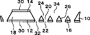
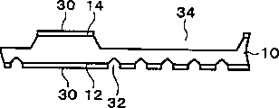
本发明的目的是制造一种高精细掩模。在基板10上形成有多个穿孔20并且它们各自的第1开口22和比第1开口22大的第2开口24之间相互连通而形成的多个穿孔20。在基板10的第1面12上形成对应于第1开口22的耐蚀刻膜30,在基板10的第1面12的相反面第2面14上,可以使2个以上的第2开口24的形成区域能连续露出,让多个穿孔20的形成区域露出。在各自的穿孔20的形成区域里,形成小穿孔36。从基板10的第1及第2面的两方,能进行具有结晶表面方向依赖性的蚀刻。

Figure 03123132

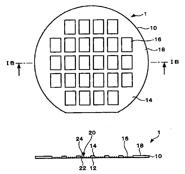
The object of the present invention is to produce a high-definition mask. A plurality of through holes 20 are formed on the substrate 10 , and the plurality of through holes 20 are formed by communicating with each other between their respective first openings 22 and second openings 24 that are larger than the first openings 22 . On the 1st face 12 of substrate 10, form the etch-resistant film 30 corresponding to the 1st opening 22, on the opposite face 2nd face 14 of the 1st face 12 of substrate 10, can make more than 2 the 2nd opening 24 The formation area can be continuously exposed, so that the formation area of a plurality of through holes 20 is exposed. In the formation regions of the respective through holes 20, small through holes 36 are formed. From both the first and second surfaces of the substrate 10, etching having crystal surface direction dependence can be performed.

Figure 03123132

Description

Mask and electroluminescent device
And manufacture method, and electronic device
Technical field
The present invention relates to mask and manufacture method thereof, electroluminescent device and manufacture method thereof, and electronic device.
Background technology
The high meticulous mask of present very demand.For example, in the manufacture process of colored organic electroluminescent (hereinafter to be referred as " EL ") device, the mask of knowing of use that just has carries out evaporation with versicolor organic material.In mask, form the perforation figure.Internal face in perforation forms tapered pipe, if when little direction is implemented evaporation, can increase the amount of incident towards the evaporation particle of perforation from the big direction of tapered tube opening towards opening, thereby corresponding little opening becomes possibility by the evaporation of Micropicture.Form the mask manufacture method of tapered pipe as this internal face in perforation, the etching method that utilizes the crystal surface directional dependence to carry out substrate is well-known.This etching method because of the existence of crystal surface directional dependence, is etched in midway and will stops, so carry out etching from big opening always when the little face of opening carries out etching.Thereby, on the big formation face of opening, generated the etch resistant film.
But when being difficult to generate the etch resistant film on the big formation face of opening, this method for making can't be suitable in practice.In addition, because of it is to carry out etchedly from big opening, be very difficult so will accurately form the position and the shape of little opening.Also have, because of will generate the etch resistant film on the formation face of big opening, so the interval between the opening that is adjacent can become greatly, it is very difficult that the height of realization mask becomes more meticulous.
Summary of the invention
One of purpose of the present invention is made high meticulous mask exactly.
(1) manufacture method relevant with the present invention be comprise this be formed with on the substrate a plurality of perforation and they separately the 1st opening and than the 2nd big opening of above-mentioned the 1st opening between be interconnected and the mask manufacture method of a plurality of perforation of forming, above-mentioned method for making comprises:
(a) on the 1st of aforesaid substrate, form the etch resistant film of corresponding the 1st opening, on the 2nd of above-mentioned the 1st opposing face of aforesaid substrate, allow the formation zone of above-mentioned a plurality of perforation expose so that the formation zone of above-mentioned the 2nd opening more than 2 can be exposed continuously.
(b) in the formation zone of separately above-mentioned perforation, form the little perforation littler than its above-mentioned perforation separately; And
(c), has the etching of crystal surface directional dependence from the above-mentioned the 1st and the 2nd two sides of aforesaid substrate.
Based on the present invention, because of allowing the formation zone of perforation expose on the 2nd of substrate, so with the 2nd go up that the difficulty that forms the etch resistant film is irrelevant to produce mask.In addition, because of the 1st the etch resistant film of going up formation corresponding to the 1st opening of substrate, so can accurately form the position and the shape of the 1st opening (than the little opening of the 2nd opening).Also have, forming on the 2nd of the 2nd opening (than the big opening of the 1st opening), because of exposing continuously in the formation zone that makes the 2nd opening more than 2, thus can dwindle interval between the 2nd adjacent opening, thereby the height of mask becomes more meticulous and just becomes possibility.
(2) in this mask manufacture method
Use Laser Processing, little air-flow (micro blast) processing, any processing method in time modulation plasma (timemodulation plasma) etching method or the machining can form the above-mentioned little perforation also littler than above-mentioned perforation.
(3) in this mask manufacture method
Use can have the etching of crystal surface directional dependence less than the 30% tetramethyl oxyammonia solution that is made into greater than 10% in weight ratio (by % weight).
(4) in this mask manufacture method
In above-mentioned (a) step, can in above-mentioned the 2nd, avoid the formation zone of above-mentioned a plurality of perforation and form above-mentioned etch resistant film.
In view of the above, the part that is covered by the etch resistant film does not have etched, thereby stays next thick-layer in substrate, so can produce the high strength mask.
(5) in this mask manufacture method
Implement after above-mentioned (b) step, implement above-mentioned (c) step again, in above-mentioned (c) step, can enlarge the above-mentioned little perforation also littler by having the above-mentioned etching of crystal surface directional dependence than above-mentioned perforation.
(6) in this mask manufacture method
Before above-mentioned (b) step and implement above-mentioned (c) step afterwards,
Before above-mentioned (b) step, from the above-mentioned the 1st and the 2nd two sides of aforesaid substrate, implement above-mentioned etching with crystal surface directional dependence, till the etching that will arrive above-mentioned the 1st side at least stops,
After above-mentioned (b) step,, can enlarge the above-mentioned little perforation also littler than above-mentioned perforation by having the above-mentioned etching of crystal surface directional dependence.
In view of the above, before forming than the also little little perforation of perforation, the formation of etching and punching is regional and can make the substrate attenuation.Therefore, form easier that the little perforation also littler than perforation becomes.
(7) in this mask manufacture method
Aforesaid substrate is a monocrystalline silicon substrate,
The the above-mentioned the 1st and the 2nd face of aforesaid substrate be reflection index (mirror index) for the face of 100},
The internal face of its above-mentioned perforation separately be the 111} face,
Above-mentioned etched above-mentioned crystal surface directional dependence is for { for the etching speed of 111} face, having the slower character of etching speed than the face of representing with the reflection index beyond this.
(8) in this mask manufacture method
Become and above-mentionedly { behind the 111} face, can stop the above-mentioned etching of above-mentioned (c) step when the etch resistant film of aforesaid substrate whole expose face.
(9) mask relevant with the present invention is based on that said method makes.
(10) relevant with the present invention mask has the substrate that forms a plurality of perforation,
The internal face that above-mentioned perforation separately is based on inclination forms, and the 1st opening and 2nd opening bigger than above-mentioned the 1st opening are communicated with,
In the side that above-mentioned the 2nd opening forms, its above-mentioned perforation separately only depends on above-mentioned internal face to distinguish with at least 1 adjacent above-mentioned perforation.
Based on the present invention, the interval between adjacent the 2nd opening becomes very little, and the figure of mask is become more meticulous by height.
(11) in this mask
Aforesaid substrate is a monocrystalline silicon substrate,
The internal face of its above-mentioned perforation separately can be that reflection index (mirror index) is { face of 111}.
(12) relevant with the present invention electroluminescent device manufacture method comprises the film forming that the use aforementioned mask is carried out luminescent material.
(13) electroluminescent device relevant with the present invention is based on that said method makes.
(14) electronic device relevant with the present invention has above-mentioned electroluminescent device.
Description of drawings
Figure 1A-Figure 1B is the mask synoptic diagram relevant with the present invention the 1st embodiment.
Fig. 2 is the partial enlarged drawing of the mask relevant with the present invention the 1st embodiment.
Fig. 3 A-Fig. 3 E is the mask making key diagram relevant with the present invention the 1st embodiment.
Fig. 4 A-Fig. 4 B is the mask making key diagram relevant with the present invention the 2nd embodiment.
Fig. 5 is the EL device manufacturing method key diagram relevant with the present invention the 3rd embodiment.
Fig. 6 A-Fig. 6 C is the one-tenth embrane method key diagram of luminescent material.
Fig. 7 is the EL equipment synoptic diagram relevant with the embodiment of the invention.
Fig. 8 is the electronic device synoptic diagram relevant with the embodiment of the invention.
Fig. 9 is the electronic device synoptic diagram relevant with the embodiment of the invention.
The embodiment of invention
Below with reference view explanation embodiments of the invention.
(the 1st embodiment)
Figure 1A-Figure 1B is the mask planimetric map relevant with the present invention the 1st embodiment.
Figure 1B is the sectional view of the line IB-IB that marks among Figure 1A.
Fig. 2 is the partial enlarged drawing of Figure 1A.Mask 1 has substrate (for example monocrystal substrate) 10 (or only being formed by substrate (for example monocrystal substrate) 10).Substrate 10 can be a monocrystalline silicon, also can be silicon wafer (silicon wafer).(the 1st and the 2nd 12,14) also can be that reflection index (mirror index) is { face of 100} on the two sides of substrate 10.And { 100} bread contains and { a plurality of of 100} face equivalence.In cubic lattice with { direction that the 100} face is vertical is exactly its { 100} orientation.
In substrate 10, form 1 (for example a plurality of) thin portion 16 at least.A plurality of thin portions 16 can become arranged.Substrate 10 also has thick 18 except that thin portion 16.Guaranteed the intensity of substrate 10 for thick 18.The edge part of substrate 10 has been avoided in the formation of thin portion 16.The edge part of substrate 10 can be thick 18.Impaled thin portion 16 because of thick 18, so thin portion 16 just is difficult to distortion.
Thin portion 16 is positioned at the position of being partial to the 1st (single face) 12 for the thickness direction of substrate 10.The bottom that promptly thin portion 16 is exactly the recess of formation on the 2nd (the 1st 12 opposing face) 14 of substrate 10.In substrate 10, approaching portion 16 and the part (thick 18) beyond its upward is with one side at the face (the 1st 12) of an opposite side of the face (the 2nd 14) that forms recess.
In substrate 10, form a plurality of perforation 20.The zone that forms perforation 20 just becomes thin portion 16.1 group of perforation 20 forms a thin portion 16.Its perforation 20 separately has been communicated with the 1st and the 2nd opening 22,24.The 1st opening 22 is formed at the 1st 12, the 2 opening 24 and is formed at the 2nd 14.The 2nd opening 24 to the 1 openings 22 are big.The polygon that is shaped as rectangle (square or rectangular) etc. of the 1st and the 2nd opening 22,24, circle, oval-shaped any one can.The shape of the 1st and the 2nd opening 22,24 both can be similarity, also can be non-similarity.
Perforation 20 internal face 26 is at least one side of the 1st and the 2nd 12,14 of substrate 10, is not the right angle but tilts.Internal face 26 can be a tabular surface.Internal face 26 is { 111} a face in the present embodiment.Substrate 10 is a monocrystalline silicon substrate, and the 1st 12 is that { during the 100} face, internal face 26 and the 1st 12 formed angle are 54.7 degree.A side of the 2nd 14, perforation 20 only depends on internal face 26 to distinguish with adjacent at least 1 perforation 20.Promptly, only exist between the adjacent perforation 20 by its internal face 26 formed bights separately a side of the 2nd 14.Based on this, the interval of adjacent the 2nd opening 24 becomes very little, and the figure of mask 1 is become more meticulous by height like this.
Fig. 3 A-Fig. 3 E is the mask making key diagram relevant with the embodiment of the invention.In the present embodiment, form above-mentioned perforation 20 grades and want prepared substrate 10 before.Substrate 10 can be a monocrystalline silicon substrate, also can be silicon wafer (silicon wafer).Substrate 10 has with reflection index (mirror the index) { surface that 100} represents.For example, the surface of substrate 10, the back side (the 1st and the 2nd 12,14) all is { 100} face.The the 1st and the 2nd 12,14 one side (for example two sides) at least of substrate 10 can be carried out mirror ultrafinish in advance.
In the explanation as Fig. 3 A, form etch resistant film 30 (for example thickness is about 1 micron) in the substrate 10.Etch resistant film 30 forms at least in the 1 12 of substrate 10, also can form in the 2nd 14.Etch resistant film 30 covers continuously in whole face (side that comprises the end that is positioned at the 1st and the 2nd 12,14) of substrate 10 and forms.Can utilize the monox that uses in the thermal oxidation method (for example wet type thermal oxidation method), silicon nitride also has silit to form etch resistant film 30.Etch resistant film 30 can be the silicon nitride film that forms from CVD, also can be gold or the chromium film that utilizes the sputter method to form.
The 1st opening 22 of the corresponding perforation 20 of etch resistant film 30 is formed on the 1st 12 of substrate 10.For example, the explanation among Fig. 3 B forms a plurality of the 1st etching mouths 32 on the 1st 12 etch resistant film 30.Each the 1st etching mouth 32 is corresponding with the shape of the 1st opening 22, and the two also can be same shape.A part of the 1st 12 is exposed in the inside of its 1st etching mouth 32 separately.A side of the 1st 12, the formation of adjacent perforation 20 zone discontinuous exposing.
On the 2nd 14 of substrate 10,, allow the formation zone of a plurality of perforation 20 expose in order to expose the formation zone of the 2nd opening 24 more than 2 continuously.When forming etch resistant film 30 on the 2nd 12, form one or more the 2nd etching mouth 34.Each the 2nd etching mouth 34 is corresponding with the formation zone of thin portion 16 among Figure 1A, and the two also can be same shape.When forming etch resistant film 30 in the 2nd 14, the part that is covered by etch resistant film 30 in the 1st and the 2nd 12,14 two sides is not etched.Thereby in substrate 10, stay thick part, so can make high strength mask 1.
The 1st etching mouth 32 separately is formed in the zone (view field) of some the 2nd etching mouth 34.Forming in the 1st and the 2nd etching mouth 32,34, can use photoetching process (phototlihography) and etching method (for example using the wet etching of fluoric acid and ammonium fluoride solution).
In the explanation as Fig. 3 C, formed the perforation 36 littler (below, claim little perforation) in the formation zone of perforation 20 separately than perforation 20.Can use laser (YAG laser for example; carbon dioxide laser) processing; little air-flow (with the method for strong jet spraying microparticles) processing; any processing method in the machining of time modulation plasma (time modulation plasma) etching method (the sidewall diaphragm that hockets forms and etching method) and use drilling machine etc. all is fit to form little perforation 36.A side of the 1st 12, little perforation 36 separately is formed at the inside of the 1st etching mouth 32 separately.
In the explanation as Fig. 3 D, the 1st and the 2nd 12,14 two sides from substrate 10 carry out etching with etchant resist 30 as mask.After forming little perforation 36, carry out etching again, so by etching, little perforation 36 is extended.In the present embodiment, (for example in etching, there is the crystal surface directional dependence, for { for the etching speed of 111} face, it is compared to { 100} face and { it is slow (for example more than 10 times that the etching speed of 110} face is wanted, be contemplated to be slow more than 100 times), be called the crystal surface directional dependence) be fine.
Use is with the aqueous slkali of organic amine series, for example, tetramethyl oxyammonia solution so that weight ratio (by % weight) is made into less than 30% (being generally about 10-20%) greater than 10% is heated to the etching that has the crystal surface directional dependence about 80 degrees centigrade to it.Perhaps, use the inorganic alkali solution except that potassium hydroxide solution, for example use ammoniacal liquor also passable.Do not contain potassium because of using, the aqueous slkali of sodium so can prevent pollution when making mask 1, like this when using mask 1 to carry out evaporation, just can prevent the pollution as the TFT substrate of evaporation object etc.In addition, the present invention does not get rid of the etching of using potassium to carry out.For example, 15% potassium hydroxide solution can be heated to 80 degree uses.
Show that in Fig. 3 D bright example is that substrate 10 is monocrystalline silicon substrate, its the 1st and the 2nd 12,14 is { 100} face, for { for the etching speed of 111} face, it is to be compared to { 100} face and { etching speed of 110} face is wanted the etching example with crystal surface directional dependence that is called of slow (for example more than 10 times, being contemplated to be slow more than 100 times).
At this moment, expose in the 1st etching mouth 32 of the 1st 12 1 sides { the 100} face is etched, and little perforation 36 is extended.Based on the etching of little perforation 36 and the expansion of carrying out stop at the 1st etching mouth 32 of etch resistant film 30.A side of the 2nd 14, expose in the 2nd etching mouth 34 { the 100} face is etched.A side of the 2nd 14, because of exposing in the zone between the adjacent little perforation 36, so this part { the 100} face is also etched.Thereby in substrate 10, can form thin portion 16.Expose face from the etch resistant film 30 of substrate 10 whole and become that { behind the 111} face, etching just stops.
Like this, just can form perforation 20.Show in Fig. 3 D in the bright example that perforation 20 internal face is all based on { 111} face and forming.If necessary, as Fig. 3 E is illustrated, can remove etch resistant film 30.When etch resistant film 30 is formed by insulator,, just can prevent to adhere to because of the particulate (particle) that static produces because of removing its cause.In addition, if necessary, according to also substrate 10 being cut opportunity etc.Based on above step, can produce the mask 1 among Fig. 1.
Based on present embodiment, expose because of on the 2nd 14 of substrate 10, making perforation 20 formation zone, so with the 2nd 14 on form that the difficulty of etch resistant film 30 is irrelevant just to produce mask 1.In addition, because of on the 1st 12 of substrate 10, forming etch resistant film 30, so can accurately form the position and the shape of the 1st opening 22 (than the little opening of the 2nd opening 24) corresponding to the 1st opening 22.Also have, forming on the 2nd 14 of the 2nd opening 24 (than the big opening of the 1st opening 22), because of the formation zone of the 2nd opening 24 more than 2 is exposed continuously, thus the interval of 24 of the 2nd adjacent openings can be dwindled, thereby the height of mask 1 become more meticulous just become possibility.
(the 2nd embodiment)
Fig. 4 A-Fig. 4 B is the mask making key diagram relevant with the present invention the 2nd embodiment.Present embodiment is carried out the step of representing among above-mentioned Fig. 3 A-Fig. 3 B.That is, on the 1st and the 2nd 12,14 of substrate 10, form etch resistant film 30, form in the etch resistant film 30 on a side of the 1st 12 in the etch resistant film 30 on the side of 32, the 2 14 in the 1st etching mouth and form the 2nd etching mouth 34.
Next step carries out the step of representing among Fig. 4 A.That is, the 1st and the 2nd 12,14 two sides from substrate 10 implement the etching with crystal surface directional dependence.Can use the aqueous slkali with organic amine series, for example, the tetramethyl oxyammonia solution so that weight ratio (by % weight) is made into less than 30% (being generally about 10-20%) greater than 10% is heated to use about 80 degrees centigrade to it.Perhaps, also can use the inorganic alkali solution except that potassium hydroxide solution, for example use ammoniacal liquor.Do not contain potassium because of using, the aqueous slkali of sodium so can prevent when making mask 1 pollution to it, like this when using mask 1 to carry out evaporation, just can prevent the pollution as the TFT substrate of evaporation object etc.In addition, the present invention does not get rid of the etching of using potassium to carry out.For example, 15% potassium hydroxide solution can be heated to 80 degrees centigrade of uses.
Show among Fig. 4 A that bright example is that substrate 10 is monocrystalline silicon substrate, its the 1st and the 2nd 12,14 is { 100} face, for { for the etching speed of 111} face, it is to be compared to { 100} face and { etching speed of 110} face is wanted the etching example with crystal surface directional dependence that is called of slow (for example more than 10 times, being contemplated to be slow more than 100 times).On the 1st 12 the side, the 1st etching mouth 32 is perforated 20 regional differentiation of each formation, because of the part of exposing is very little, so { etching on the 111} face will stop.Simultaneously, the 2nd etching mouth 34 is because of the continuous opening in formation zone of the perforation more than 2 20, so exposed portions serve is very big, it is very dark that etching will be carried out, and can make substrate 10 become very thin.Etching is that tube is managed the gentle time of its etching solution and carried out.Till this etching will proceed to etching on the 1st 12 the side at least and stops.
Next, as the explanation of Fig. 4 B, (in the 1st etching mouth 32) forms than the 20 little perforation 36 of boring a hole in the formation zone of perforation 20.Present embodiment just forms little perforation 36 because of substrate 10 is become after very thin, so can modulate plasma (time modulationplasma) etching method (the sidewall diaphragm that hockets forms and etching method) service time or use the machining of drilling machine etc. to form little perforation 36.In addition the content that illustrates among content and the 1st embodiment Fig. 3 C is identical.
After this content that illustrates among Fig. 3 D and Fig. 3 E among step and the 1st embodiment is identical.That is, the etching by the crystal surface directional dependence enlarges little perforation 36.Present embodiment also can produce the mask 1 among Fig. 3 E.The content that has illustrated among other content and the 1st embodiment is the same.
(the 3rd embodiment)
Fig. 5 is the EL device manufacturing method key diagram relevant with the present invention the 3rd embodiment.Form magnetic film 52 in the mask of representing among Fig. 51.Magnetic film 52 can be used iron, cobalt, and ferromagnetic materials such as nickel are made.Perhaps, use Ni, Co, Fe, or contain the magnetic metal materials such as stainless steel alloy of Fe composition, or the two synthetic material of magnetic metal material and nonmagnetic material can be made magnetic film 52.The detailed part of other of relevant mask 1 is described in the 1st and the 2nd embodiment.
Present embodiment uses 1 pair of substrate of mask 54 to carry out the luminescent material film forming.Substrate 54 is owing to be EL device (for example organic El device), think the transparency carrier of glass substrate class.In substrate 54,, form electrode 56 (for example constituting transparency electrode) and hole transporting layer 58 by ITO etc. as the explanation among Fig. 6 A.And can form electron supplying layer.In substrate 54, towards the 1st the 12 configuration mask 1 that forms the 1st opening 22.The tabular surface that is mask 1 is facing to substrate 54 1 sides.Magnetite 50 is equipped with at the back of substrate 54, attracts the magnetic film 52 in the mask 1.Like this, crooked even mask 1 produces, also can correct.
Fig. 6 A-Fig. 6 C is the one-tenth embrane method key diagram to luminescent material.Luminescent material is an organic material, as low molecule organic material Alq3 is arranged, and as macromolecule organic material PPV is arranged.The film forming ability of luminescent material is realized by evaporation.For example, as Fig. 6 A, by mask 1 the red illuminating material limit is formed the graph edge film forming and form red light emitting layer 60.Then,, mask 1 is moved, the green luminescent material limit is formed the graph edge film forming form green light emitting layer 62 as Fig. 6 B.At last,, mask 1 is moved once more, the blue emitting material limit is formed the graph edge film forming form blue light-emitting layer 64 as Fig. 6 C.
Fig. 7 is the EL device synoptic diagram relevant with the embodiment of the invention.EL device (for example organic El device) has substrate 54, electrode 56, hole transporting layer 58, luminescent layer 60,62,64.At luminescent layer 60,62, form electrode 66 on 64.Electrode 66 such as be cathode electrode.EL device (EL panel) becomes display device (display).
As the electronic device with EL device relevant with the embodiment of the invention, express notebook PC 1000 among Fig. 8, express mobile phone 2000 among Fig. 9.
The present invention is not limited to by the above embodiments, is possible based on its various distortion.For example, the present invention comprises formation that embodiment illustrated and identical in fact therewith formation (for example, function, method and result have identical formation with the present invention, perhaps purpose and result have identical formation with the present invention).The present invention also comprises the formation of changing the non-intrinsically safe part in the formation that embodiment illustrated.The present invention also comprises the formation that the formation that has illustrated with embodiment plays the same purpose effect, or can reach the formation of same purpose.The present invention is also contained in total technology additional in the formation that embodiment illustrated and constitutes.

Claims (14)

1. mask manufacture method comprises following steps: be formed with on the substrate a plurality of perforation and they separately the 1st opening and than the 2nd big opening of above-mentioned the 1st opening between be interconnected, above-mentioned method for making also comprises following steps:
(a) the 1st of aforesaid substrate the etch resistant film that go up to form corresponding to the 1st opening on the 2nd of above-mentioned the 1st opposing face of aforesaid substrate, allows the formation zone of above-mentioned a plurality of perforation expose so that the formation zone of above-mentioned the 2nd opening more than 2 can be exposed continuously.
(b) in the formation zone of separately above-mentioned perforation, form the little perforation littler than its above-mentioned perforation separately; And
(c) has the etching of crystal surface directional dependence from the above-mentioned the 1st and the 2nd two sides of aforesaid substrate.
2. the described mask manufacture method of claim 1 is characterized in that,
Use Laser Processing, little air-flow processing, any processing method in time modulation plasma etching method or the machining forms the above-mentioned little perforation also littler than above-mentioned perforation.
3. the described mask manufacture method of claim 1 is characterized in that,
Use has the etching of crystal surface directional dependence less than the 30% tetramethyl oxyammonia solution that is made into greater than 10% with weight ratio.
4. the described mask manufacture method of claim 1 is characterized in that,
In above-mentioned (a) step, in above-mentioned the 2nd, avoid the formation zone of above-mentioned a plurality of perforation and form above-mentioned etch resistant film.
5. claim 1 is characterized in that to the mask manufacture method described in each of claim 4,
Implement after above-mentioned (b) step, implement above-mentioned (c) step again, in above-mentioned (c) step,, enlarge the above-mentioned little perforation also littler than above-mentioned perforation based on above-mentioned etching with crystal surface directional dependence.
6. claim 1 is characterized in that to the mask manufacture method described in each of claim 4,
Before above-mentioned (b) step and implement above-mentioned (c) step afterwards,
Before above-mentioned (b) step, from the above-mentioned the 1st and the 2nd two sides of aforesaid substrate, implement the above-mentioned etching that the crystal surface directional dependence is arranged, to arrive at least till etching on above-mentioned the 1st side stops,
After above-mentioned (b) step,, enlarge the above-mentioned little perforation also littler than above-mentioned perforation based on above-mentioned etching with crystal surface directional dependence.
7. claim 1 is characterized in that to the mask manufacture method described in each of claim 4,
Aforesaid substrate is a monocrystalline silicon substrate,
The the above-mentioned the 1st and the 2nd face of aforesaid substrate be reflection index (mirror index) for the face of 100},
The internal face of its above-mentioned perforation separately be the 111} face,
Above-mentioned etched above-mentioned crystal surface directional dependence is for { for the etching speed of 111} face, having the slower character of etching speed than the face of representing with the reflection index beyond this.
8. the described mask manufacture method of claim 7 is characterized in that,
Exposing face from the etch resistant film of aforesaid substrate whole becomes and above-mentionedly { behind the 111} face, stops the above-mentioned etching of above-mentioned (c) step.
9. mask of making based on the described method of claim 1.
10. a mask has the substrate that forms a plurality of perforation,
The internal face that above-mentioned perforation separately is based on inclination forms, and the 1st opening and 2nd opening bigger than above-mentioned the 1st opening are communicated with,
In the side that forms above-mentioned the 2nd opening, its above-mentioned perforation separately only depends on above-mentioned internal face and adjacent at least 1 above-mentioned punch block to separate.
11. the described mask of claim 10 is characterized in that,
Aforesaid substrate is a monocrystalline silicon substrate,
The internal face of its above-mentioned perforation separately is that reflection index is { 111} a face.
12. one kind comprises and uses accessory rights requirement 9 to the mask described in each of claim 11, carries out the electroluminescent device manufacture method of luminescent material film forming.
13. electroluminescent device of making based on the described method of claim 12.
14. electronic device with the described electroluminescent device of claim 13.
CNB031231322A 2002-04-17 2003-04-17 Mask and electroluminescent device and method for mfg. same, and electronic apparatus Expired - Lifetime CN1249521C (en)

Applications Claiming Priority (3)

Application Number Priority Date Filing Date Title
JP2002114682A JP3856123B2 (en) 2002-04-17 2002-04-17 MASK AND ITS MANUFACTURING METHOD, ELECTROLUMINESCENT DEVICE, ITS MANUFACTURING METHOD, AND ELECTRONIC DEVICE
JP114682/02 2002-04-17
JP114682/2002 2002-04-17

Publications (2)

Publication Number Publication Date
CN1452010A true CN1452010A (en) 2003-10-29
CN1249521C CN1249521C (en) 2006-04-05

Family

ID=29243394

Family Applications (1)

Application Number Title Priority Date Filing Date
CNB031231322A Expired - Lifetime CN1249521C (en) 2002-04-17 2003-04-17 Mask and electroluminescent device and method for mfg. same, and electronic apparatus

Country Status (5)

Country Link
US (1) US7387739B2 (en)
JP (1) JP3856123B2 (en)
KR (1) KR100503616B1 (en)
CN (1) CN1249521C (en)
TW (1) TW593712B (en)

Cited By (4)

* Cited by examiner, † Cited by third party
Publication number Priority date Publication date Assignee Title
CN103208592A (en) * 2012-01-16 2013-07-17 昆山允升吉光电科技有限公司 Evaporating method of organic light-emitting diode
CN104532183A (en) * 2015-01-26 2015-04-22 深圳市华星光电技术有限公司 Manufacturing method of high-precision mask
CN114481085A (en) * 2020-10-28 2022-05-13 佳能株式会社 Vapor deposition mask and method of manufacturing apparatus using the same
TWI767181B (en) * 2019-03-27 2022-06-11 日商日立金屬股份有限公司 Coating sheet for metal mask and metal mask

Families Citing this family (12)

* Cited by examiner, † Cited by third party
Publication number Priority date Publication date Assignee Title
JP3775493B2 (en) * 2001-09-20 2006-05-17 セイコーエプソン株式会社 Mask manufacturing method
KR100903818B1 (en) * 2003-11-12 2009-06-25 에스케이씨 주식회사 Manufacturing method of shadow mask for organic light emitting device
JP3794407B2 (en) 2003-11-17 2006-07-05 セイコーエプソン株式会社 Mask, mask manufacturing method, display device manufacturing method, organic EL display device manufacturing method, organic EL device, and electronic apparatus
US20080118707A1 (en) * 2006-11-22 2008-05-22 Advanced Chip Engineering Technology Inc. Method and structure of pattern mask for dry etching
DE102007031549B4 (en) 2007-07-06 2021-07-08 Robert Bosch Gmbh Single crystal silicon device and method of making a single crystal silicon device
ITMI20080615A1 (en) * 2008-04-08 2009-10-09 St Microelectronics Srl METHOD FOR THE REALIZATION OF A IMPROVED EFFICIENT MICROREACTOR FOR AN ENERGY PRODUCTION SYSTEM FOR PORTABLE MICROCELL APPLICATIONS
JP6155650B2 (en) * 2013-01-11 2017-07-05 大日本印刷株式会社 Manufacturing method of vapor deposition mask
CN104213072B (en) * 2013-05-31 2016-09-14 旭晖应用材料股份有限公司 Composite mask and manufacturing method thereof
CN110699637B (en) * 2019-10-17 2021-03-23 昆山国显光电有限公司 Mask manufacturing method, mask and display panel manufacturing method
CN113088875B (en) * 2021-04-02 2022-12-13 京东方科技集团股份有限公司 Mask and preparation method thereof
JP2025034168A (en) * 2023-08-30 2025-03-13 大日本印刷株式会社 Mask and mask manufacturing method
WO2025110105A1 (en) * 2023-11-22 2025-05-30 大日本印刷株式会社 Mask and method for producing mask

Family Cites Families (8)

* Cited by examiner, † Cited by third party
Publication number Priority date Publication date Assignee Title
US4961821A (en) * 1989-11-22 1990-10-09 Xerox Corporation Ode through holes and butt edges without edge dicing
JPH04236758A (en) 1991-01-16 1992-08-25 Oki Electric Ind Co Ltd Mask for vapor deposition
JP3755228B2 (en) * 1997-04-14 2006-03-15 株式会社ニコン Charged particle beam exposure system
US6322201B1 (en) * 1997-10-22 2001-11-27 Hewlett-Packard Company Printhead with a fluid channel therethrough
JP3209169B2 (en) * 1997-11-28 2001-09-17 日本電気株式会社 Method of forming gate electrode
JP2001185350A (en) 1999-12-24 2001-07-06 Sanyo Electric Co Ltd Worn mask, its manufacturing method, electroluminescent display device and its manufacturing method
JP2002004034A (en) 2000-06-23 2002-01-09 Sanyo Electric Co Ltd Mask for vapor deposition and its production method
JP3775493B2 (en) * 2001-09-20 2006-05-17 セイコーエプソン株式会社 Mask manufacturing method

Cited By (5)

* Cited by examiner, † Cited by third party
Publication number Priority date Publication date Assignee Title
CN103208592A (en) * 2012-01-16 2013-07-17 昆山允升吉光电科技有限公司 Evaporating method of organic light-emitting diode
CN104532183A (en) * 2015-01-26 2015-04-22 深圳市华星光电技术有限公司 Manufacturing method of high-precision mask
TWI767181B (en) * 2019-03-27 2022-06-11 日商日立金屬股份有限公司 Coating sheet for metal mask and metal mask
CN114481085A (en) * 2020-10-28 2022-05-13 佳能株式会社 Vapor deposition mask and method of manufacturing apparatus using the same
US12178111B2 (en) 2020-10-28 2024-12-24 Canon Kabushiki Kaisha Vapor deposition mask and method of manufacturing device using vapor deposition mask

Also Published As

Publication number Publication date
US7387739B2 (en) 2008-06-17
JP3856123B2 (en) 2006-12-13
US20040026360A1 (en) 2004-02-12
JP2003308972A (en) 2003-10-31
TW200307052A (en) 2003-12-01
KR20030082486A (en) 2003-10-22
KR100503616B1 (en) 2005-07-22
CN1249521C (en) 2006-04-05
TW593712B (en) 2004-06-21

Similar Documents

Publication Publication Date Title
CN1214697C (en) Mask and its mfg. method, electroluminance device and its mfg. method and electronic machine
CN1452010A (en) Mask and electroluminescent device and method for mfg. same, and electronic apparatus
JP2019521380A (en) Diodes providing asymmetry and stability in fluidic assembly
CN103456854A (en) Light-emitting element with graphical interface and manufacturing method thereof
US20110294295A1 (en) Method for making three-dimensional nano-structure array
CN101325234A (en) Method for making photonic crystal structure GaN-based light-emitting diode
CN109671734A (en) Display panel and its manufacturing method
WO2006088228A1 (en) Semiconductor luminous element and method for manufacture thereof
CN109962083A (en) A flexible color Micro-LED preparation method and prepared product
CN104241475A (en) Light-emitting diode chip and manufacturing method thereof
CN105957801A (en) Gallium nitride nanocone and gallium nitride nanorod mixed array manufacturing method
CN106784218B (en) LED chip and manufacturing method thereof
CN1630438A (en) Mask and manufacturing method thereof, organic electroluminescent device and manufacturing method thereof, electronic device
US20230130620A1 (en) High-resolution ultra-thin led display for ar and vr devices and manufacturing method thereof
CN102593280B (en) LED (Light Emitting Diode) surface patterning method
WO2012091325A2 (en) Method for manufacturing light-emitting diode using nano-structures and light-emitting diode manufactured thereby
CN104465926B (en) Graphical sapphire substrate and light emitting diode
CN1877872A (en) Photonic crystal-structural GaN-base blue LED structure and method for fabricating same
KR102206894B1 (en) Deposition Metal Mask for OLED and Manufacturing Method of the same
CN107123705B (en) Preparation method of light-emitting diode
CN102130221A (en) Method for forming light-emitting diodes
CN104485402B (en) Method for manufacturing patterned sapphire substrate
CN100373187C (en) Color filter substrate and manufacturing method thereof
CN203021642U (en) OLED (Organic Light Emitting Diode) evaporating hood
KR100871649B1 (en) Sapphire substrate patterning method of light emitting diode

Legal Events

Date Code Title Description
C06 Publication
PB01 Publication
C10 Entry into substantive examination
SE01 Entry into force of request for substantive examination
C14 Grant of patent or utility model
GR01 Patent grant
C41 Transfer of patent application or patent right or utility model
TR01 Transfer of patent right

Effective date of registration: 20160612

Address after: 100015 Jiuxianqiao Road, Beijing, No. 10, No.

Patentee after: BOE TECHNOLOGY GROUP Co.,Ltd.

Address before: Hongkong, China

Patentee before: BOE Technology (Hongkong) Co.,Ltd.

Effective date of registration: 20160612

Address after: Hongkong, China

Patentee after: BOE Technology (Hongkong) Co.,Ltd.

Address before: Tokyo, Japan

Patentee before: Seiko Epson Corp.

CX01 Expiry of patent term

Granted publication date: 20060405

CX01 Expiry of patent term