CN1331247C - Electroluminescent devices - Google Patents
Electroluminescent devices Download PDFInfo
- Publication number
- CN1331247C CN1331247C CNB998039810A CN99803981A CN1331247C CN 1331247 C CN1331247 C CN 1331247C CN B998039810 A CNB998039810 A CN B998039810A CN 99803981 A CN99803981 A CN 99803981A CN 1331247 C CN1331247 C CN 1331247C
- Authority
- CN
- China
- Prior art keywords
- composition
- layer
- electroluminescent device
- light
- carrier
- Prior art date
- Legal status (The legal status is an assumption and is not a legal conclusion. Google has not performed a legal analysis and makes no representation as to the accuracy of the status listed.)
- Expired - Lifetime
Links
- 239000000203 mixture Substances 0.000 claims abstract description 251
- 239000004065 semiconductor Substances 0.000 claims abstract description 31
- 239000002800 charge carrier Substances 0.000 claims abstract description 25
- 238000002347 injection Methods 0.000 claims description 61
- 239000007924 injection Substances 0.000 claims description 61
- 229920000642 polymer Polymers 0.000 claims description 43
- 229920000553 poly(phenylenevinylene) Polymers 0.000 claims description 31
- 238000004768 lowest unoccupied molecular orbital Methods 0.000 claims description 22
- 230000003287 optical effect Effects 0.000 claims description 18
- 229920000547 conjugated polymer Polymers 0.000 claims description 11
- 239000004615 ingredient Substances 0.000 claims description 5
- 239000011368 organic material Substances 0.000 claims description 5
- 125000003368 amide group Chemical group 0.000 claims description 3
- 239000010410 layer Substances 0.000 description 243
- 239000000463 material Substances 0.000 description 66
- 238000004770 highest occupied molecular orbital Methods 0.000 description 33
- 230000032258 transport Effects 0.000 description 31
- 230000005525 hole transport Effects 0.000 description 16
- 238000000034 method Methods 0.000 description 12
- 229920000144 PEDOT:PSS Polymers 0.000 description 10
- 229920001577 copolymer Polymers 0.000 description 10
- 239000000243 solution Substances 0.000 description 9
- 239000000956 alloy Substances 0.000 description 7
- 229910045601 alloy Inorganic materials 0.000 description 7
- 238000000295 emission spectrum Methods 0.000 description 7
- 230000002349 favourable effect Effects 0.000 description 7
- 238000006467 substitution reaction Methods 0.000 description 7
- IJGRMHOSHXDMSA-UHFFFAOYSA-N Atomic nitrogen Chemical compound N#N IJGRMHOSHXDMSA-UHFFFAOYSA-N 0.000 description 6
- 229910010199 LiAl Inorganic materials 0.000 description 6
- YXFVVABEGXRONW-UHFFFAOYSA-N Toluene Chemical compound CC1=CC=CC=C1 YXFVVABEGXRONW-UHFFFAOYSA-N 0.000 description 6
- 238000000151 deposition Methods 0.000 description 6
- 230000000694 effects Effects 0.000 description 6
- 238000005259 measurement Methods 0.000 description 6
- 238000002156 mixing Methods 0.000 description 6
- 238000000926 separation method Methods 0.000 description 6
- 230000008021 deposition Effects 0.000 description 5
- 238000005516 engineering process Methods 0.000 description 5
- 229910052751 metal Inorganic materials 0.000 description 5
- 239000002184 metal Substances 0.000 description 5
- 229910052757 nitrogen Inorganic materials 0.000 description 5
- 239000002904 solvent Substances 0.000 description 5
- 239000000126 substance Substances 0.000 description 5
- CTQNGGLPUBDAKN-UHFFFAOYSA-N O-Xylene Chemical compound CC1=CC=CC=C1C CTQNGGLPUBDAKN-UHFFFAOYSA-N 0.000 description 4
- 229920000109 alkoxy-substituted poly(p-phenylene vinylene) Polymers 0.000 description 4
- 230000015572 biosynthetic process Effects 0.000 description 4
- 150000002220 fluorenes Chemical class 0.000 description 4
- 238000010438 heat treatment Methods 0.000 description 4
- 238000005424 photoluminescence Methods 0.000 description 4
- -1 poly (phenylenevinylene) Polymers 0.000 description 4
- 230000008569 process Effects 0.000 description 4
- 229920001897 terpolymer Polymers 0.000 description 4
- OKKJLVBELUTLKV-UHFFFAOYSA-N Methanol Chemical compound OC OKKJLVBELUTLKV-UHFFFAOYSA-N 0.000 description 3
- ZMXDDKWLCZADIW-UHFFFAOYSA-N N,N-Dimethylformamide Chemical compound CN(C)C=O ZMXDDKWLCZADIW-UHFFFAOYSA-N 0.000 description 3
- WTKZEGDFNFYCGP-UHFFFAOYSA-N Pyrazole Chemical compound C=1C=NNC=1 WTKZEGDFNFYCGP-UHFFFAOYSA-N 0.000 description 3
- 239000002253 acid Substances 0.000 description 3
- 238000006243 chemical reaction Methods 0.000 description 3
- 230000021615 conjugation Effects 0.000 description 3
- 238000009792 diffusion process Methods 0.000 description 3
- 238000010790 dilution Methods 0.000 description 3
- 239000012895 dilution Substances 0.000 description 3
- 239000011521 glass Substances 0.000 description 3
- 230000006872 improvement Effects 0.000 description 3
- 150000002739 metals Chemical class 0.000 description 3
- 239000006069 physical mixture Substances 0.000 description 3
- 238000006116 polymerization reaction Methods 0.000 description 3
- 238000001228 spectrum Methods 0.000 description 3
- PAYRUJLWNCNPSJ-UHFFFAOYSA-N Aniline Chemical compound NC1=CC=CC=C1 PAYRUJLWNCNPSJ-UHFFFAOYSA-N 0.000 description 2
- GPYKQOCYDCMGOA-UHFFFAOYSA-N CCCCCC[O] Chemical compound CCCCCC[O] GPYKQOCYDCMGOA-UHFFFAOYSA-N 0.000 description 2
- HEDRZPFGACZZDS-UHFFFAOYSA-N Chloroform Chemical compound ClC(Cl)Cl HEDRZPFGACZZDS-UHFFFAOYSA-N 0.000 description 2
- LYCAIKOWRPUZTN-UHFFFAOYSA-N Ethylene glycol Chemical compound OCCO LYCAIKOWRPUZTN-UHFFFAOYSA-N 0.000 description 2
- CDBYLPFSWZWCQE-UHFFFAOYSA-L Sodium Carbonate Chemical compound [Na+].[Na+].[O-]C([O-])=O CDBYLPFSWZWCQE-UHFFFAOYSA-L 0.000 description 2
- 229910052782 aluminium Inorganic materials 0.000 description 2
- 238000013459 approach Methods 0.000 description 2
- 125000005605 benzo group Chemical group 0.000 description 2
- QARVLSVVCXYDNA-UHFFFAOYSA-N bromobenzene Chemical compound BrC1=CC=CC=C1 QARVLSVVCXYDNA-UHFFFAOYSA-N 0.000 description 2
- 239000003795 chemical substances by application Substances 0.000 description 2
- 239000012141 concentrate Substances 0.000 description 2
- 239000000470 constituent Substances 0.000 description 2
- 238000004821 distillation Methods 0.000 description 2
- 238000001704 evaporation Methods 0.000 description 2
- 230000008020 evaporation Effects 0.000 description 2
- 230000005284 excitation Effects 0.000 description 2
- 125000003983 fluorenyl group Chemical group C1(=CC=CC=2C3=CC=CC=C3CC12)* 0.000 description 2
- 239000012535 impurity Substances 0.000 description 2
- AMGQUBHHOARCQH-UHFFFAOYSA-N indium;oxotin Chemical compound [In].[Sn]=O AMGQUBHHOARCQH-UHFFFAOYSA-N 0.000 description 2
- 238000004020 luminiscence type Methods 0.000 description 2
- 238000004519 manufacturing process Methods 0.000 description 2
- 230000007246 mechanism Effects 0.000 description 2
- 230000004048 modification Effects 0.000 description 2
- 238000012986 modification Methods 0.000 description 2
- 238000004776 molecular orbital Methods 0.000 description 2
- 239000000178 monomer Substances 0.000 description 2
- 239000012044 organic layer Substances 0.000 description 2
- JMANVNJQNLATNU-UHFFFAOYSA-N oxalonitrile Chemical compound N#CC#N JMANVNJQNLATNU-UHFFFAOYSA-N 0.000 description 2
- 229920001467 poly(styrenesulfonates) Polymers 0.000 description 2
- 229920000767 polyaniline Polymers 0.000 description 2
- 239000013047 polymeric layer Substances 0.000 description 2
- 238000010791 quenching Methods 0.000 description 2
- 230000000171 quenching effect Effects 0.000 description 2
- 239000011877 solvent mixture Substances 0.000 description 2
- 239000000758 substrate Substances 0.000 description 2
- 229920002554 vinyl polymer Polymers 0.000 description 2
- 238000004832 voltammetry Methods 0.000 description 2
- UHXOHPVVEHBKKT-UHFFFAOYSA-N 1-(2,2-diphenylethenyl)-4-[4-(2,2-diphenylethenyl)phenyl]benzene Chemical compound C=1C=C(C=2C=CC(C=C(C=3C=CC=CC=3)C=3C=CC=CC=3)=CC=2)C=CC=1C=C(C=1C=CC=CC=1)C1=CC=CC=C1 UHXOHPVVEHBKKT-UHFFFAOYSA-N 0.000 description 1
- UOPGXWZUDYOQEJ-UHFFFAOYSA-N 1-bromo-9,9-dioctylfluorene Chemical compound BrC1=CC=CC=2C3=CC=CC=C3C(C1=2)(CCCCCCCC)CCCCCCCC UOPGXWZUDYOQEJ-UHFFFAOYSA-N 0.000 description 1
- 229910017073 AlLi Inorganic materials 0.000 description 1
- KONBZFLEPZQVFS-UHFFFAOYSA-N BrN1SC2=C(C=N1)C=CC(=C2)Br Chemical compound BrN1SC2=C(C=N1)C=CC(=C2)Br KONBZFLEPZQVFS-UHFFFAOYSA-N 0.000 description 1
- MYMOFIZGZYHOMD-UHFFFAOYSA-N Dioxygen Chemical compound O=O MYMOFIZGZYHOMD-UHFFFAOYSA-N 0.000 description 1
- 101100136092 Drosophila melanogaster peng gene Proteins 0.000 description 1
- 239000004593 Epoxy Substances 0.000 description 1
- KRHYYFGTRYWZRS-UHFFFAOYSA-M Fluoride anion Chemical compound [F-] KRHYYFGTRYWZRS-UHFFFAOYSA-M 0.000 description 1
- 229920001609 Poly(3,4-ethylenedioxythiophene) Polymers 0.000 description 1
- 229920000265 Polyparaphenylene Polymers 0.000 description 1
- 239000004793 Polystyrene Substances 0.000 description 1
- 229910052772 Samarium Inorganic materials 0.000 description 1
- BLRPTPMANUNPDV-UHFFFAOYSA-N Silane Chemical compound [SiH4] BLRPTPMANUNPDV-UHFFFAOYSA-N 0.000 description 1
- 229910052771 Terbium Inorganic materials 0.000 description 1
- 229910052769 Ytterbium Inorganic materials 0.000 description 1
- 238000010521 absorption reaction Methods 0.000 description 1
- 238000000862 absorption spectrum Methods 0.000 description 1
- 239000000654 additive Substances 0.000 description 1
- 230000000996 additive effect Effects 0.000 description 1
- 230000002776 aggregation Effects 0.000 description 1
- 238000004220 aggregation Methods 0.000 description 1
- 239000004411 aluminium Substances 0.000 description 1
- XAGFODPZIPBFFR-UHFFFAOYSA-N aluminium Chemical compound [Al] XAGFODPZIPBFFR-UHFFFAOYSA-N 0.000 description 1
- 238000004458 analytical method Methods 0.000 description 1
- 239000010405 anode material Substances 0.000 description 1
- 125000000732 arylene group Chemical group 0.000 description 1
- 239000012298 atmosphere Substances 0.000 description 1
- 230000008901 benefit Effects 0.000 description 1
- 125000001797 benzyl group Chemical group [H]C1=C([H])C([H])=C(C([H])=C1[H])C([H])([H])* 0.000 description 1
- 230000005540 biological transmission Effects 0.000 description 1
- GDTBXPJZTBHREO-UHFFFAOYSA-N bromine Substances BrBr GDTBXPJZTBHREO-UHFFFAOYSA-N 0.000 description 1
- 229910052794 bromium Inorganic materials 0.000 description 1
- 229910052791 calcium Inorganic materials 0.000 description 1
- 125000002843 carboxylic acid group Chemical group 0.000 description 1
- 238000007796 conventional method Methods 0.000 description 1
- 229910052802 copper Inorganic materials 0.000 description 1
- 238000010586 diagram Methods 0.000 description 1
- 229910001882 dioxygen Inorganic materials 0.000 description 1
- TUJWIYZCAPMHSA-UHFFFAOYSA-N dipentylphosphoryloxybenzene Chemical compound CCCCCP(=O)(CCCCC)OC1=CC=CC=C1 TUJWIYZCAPMHSA-UHFFFAOYSA-N 0.000 description 1
- 238000006073 displacement reaction Methods 0.000 description 1
- 238000009826 distribution Methods 0.000 description 1
- 230000005684 electric field Effects 0.000 description 1
- 238000002848 electrochemical method Methods 0.000 description 1
- 230000005518 electrochemistry Effects 0.000 description 1
- 238000005538 encapsulation Methods 0.000 description 1
- 150000002148 esters Chemical class 0.000 description 1
- 230000007717 exclusion Effects 0.000 description 1
- 239000004744 fabric Substances 0.000 description 1
- 125000001841 imino group Chemical group [H]N=* 0.000 description 1
- 229910052738 indium Inorganic materials 0.000 description 1
- 230000003993 interaction Effects 0.000 description 1
- 239000011229 interlayer Substances 0.000 description 1
- 229910052745 lead Inorganic materials 0.000 description 1
- 229910052749 magnesium Inorganic materials 0.000 description 1
- 229910052748 manganese Inorganic materials 0.000 description 1
- 230000007935 neutral effect Effects 0.000 description 1
- 150000004767 nitrides Chemical class 0.000 description 1
- 238000005457 optimization Methods 0.000 description 1
- AHLBNYSZXLDEJQ-FWEHEUNISA-N orlistat Chemical compound CCCCCCCCCCC[C@H](OC(=O)[C@H](CC(C)C)NC=O)C[C@@H]1OC(=O)[C@H]1CCCCCC AHLBNYSZXLDEJQ-FWEHEUNISA-N 0.000 description 1
- 230000003647 oxidation Effects 0.000 description 1
- 238000007254 oxidation reaction Methods 0.000 description 1
- 239000001301 oxygen Substances 0.000 description 1
- 229910052760 oxygen Inorganic materials 0.000 description 1
- NFHFRUOZVGFOOS-UHFFFAOYSA-N palladium;triphenylphosphane Chemical compound [Pd].C1=CC=CC=C1P(C=1C=CC=CC=1)C1=CC=CC=C1.C1=CC=CC=C1P(C=1C=CC=CC=1)C1=CC=CC=C1.C1=CC=CC=C1P(C=1C=CC=CC=1)C1=CC=CC=C1.C1=CC=CC=C1P(C=1C=CC=CC=1)C1=CC=CC=C1 NFHFRUOZVGFOOS-UHFFFAOYSA-N 0.000 description 1
- 230000000149 penetrating effect Effects 0.000 description 1
- 238000005191 phase separation Methods 0.000 description 1
- HXITXNWTGFUOAU-UHFFFAOYSA-N phenylboronic acid Chemical compound OB(O)C1=CC=CC=C1 HXITXNWTGFUOAU-UHFFFAOYSA-N 0.000 description 1
- 229920002959 polymer blend Polymers 0.000 description 1
- 229920002223 polystyrene Polymers 0.000 description 1
- 229960002796 polystyrene sulfonate Drugs 0.000 description 1
- 239000011970 polystyrene sulfonate Substances 0.000 description 1
- 150000004032 porphyrins Chemical class 0.000 description 1
- 229910052700 potassium Inorganic materials 0.000 description 1
- 238000005381 potential energy Methods 0.000 description 1
- 238000001556 precipitation Methods 0.000 description 1
- 238000012545 processing Methods 0.000 description 1
- 230000001737 promoting effect Effects 0.000 description 1
- MCJGNVYPOGVAJF-UHFFFAOYSA-N quinolin-8-ol Chemical compound C1=CN=C2C(O)=CC=CC2=C1 MCJGNVYPOGVAJF-UHFFFAOYSA-N 0.000 description 1
- 239000012857 radioactive material Substances 0.000 description 1
- 239000000376 reactant Substances 0.000 description 1
- 238000001953 recrystallisation Methods 0.000 description 1
- 238000010992 reflux Methods 0.000 description 1
- 238000005204 segregation Methods 0.000 description 1
- 239000005266 side chain polymer Substances 0.000 description 1
- 229910000077 silane Inorganic materials 0.000 description 1
- 229910052709 silver Inorganic materials 0.000 description 1
- 150000003384 small molecules Chemical class 0.000 description 1
- 229910000029 sodium carbonate Inorganic materials 0.000 description 1
- 238000000935 solvent evaporation Methods 0.000 description 1
- 238000004528 spin coating Methods 0.000 description 1
- 238000003756 stirring Methods 0.000 description 1
- 229910052712 strontium Inorganic materials 0.000 description 1
- 238000012360 testing method Methods 0.000 description 1
- 229910052718 tin Inorganic materials 0.000 description 1
- XOLBLPGZBRYERU-UHFFFAOYSA-N tin dioxide Chemical compound O=[Sn]=O XOLBLPGZBRYERU-UHFFFAOYSA-N 0.000 description 1
- 229910001887 tin oxide Inorganic materials 0.000 description 1
- 229910052719 titanium Inorganic materials 0.000 description 1
- 229910052721 tungsten Inorganic materials 0.000 description 1
- 238000001429 visible spectrum Methods 0.000 description 1
- 229910052725 zinc Inorganic materials 0.000 description 1
- 229910052726 zirconium Inorganic materials 0.000 description 1
Images


Classifications
-
- C—CHEMISTRY; METALLURGY
- C09—DYES; PAINTS; POLISHES; NATURAL RESINS; ADHESIVES; COMPOSITIONS NOT OTHERWISE PROVIDED FOR; APPLICATIONS OF MATERIALS NOT OTHERWISE PROVIDED FOR
- C09K—MATERIALS FOR MISCELLANEOUS APPLICATIONS, NOT PROVIDED FOR ELSEWHERE
- C09K11/00—Luminescent, e.g. electroluminescent, chemiluminescent materials
- C09K11/06—Luminescent, e.g. electroluminescent, chemiluminescent materials containing organic luminescent materials
-
- H—ELECTRICITY
- H10—SEMICONDUCTOR DEVICES; ELECTRIC SOLID-STATE DEVICES NOT OTHERWISE PROVIDED FOR
- H10K—ORGANIC ELECTRIC SOLID-STATE DEVICES
- H10K85/00—Organic materials used in the body or electrodes of devices covered by this subclass
- H10K85/10—Organic polymers or oligomers
- H10K85/111—Organic polymers or oligomers comprising aromatic, heteroaromatic, or aryl chains, e.g. polyaniline, polyphenylene or polyphenylene vinylene
- H10K85/115—Polyfluorene; Derivatives thereof
-
- H—ELECTRICITY
- H05—ELECTRIC TECHNIQUES NOT OTHERWISE PROVIDED FOR
- H05B—ELECTRIC HEATING; ELECTRIC LIGHT SOURCES NOT OTHERWISE PROVIDED FOR; CIRCUIT ARRANGEMENTS FOR ELECTRIC LIGHT SOURCES, IN GENERAL
- H05B33/00—Electroluminescent light sources
- H05B33/12—Light sources with substantially two-dimensional radiating surfaces
- H05B33/14—Light sources with substantially two-dimensional radiating surfaces characterised by the chemical or physical composition or the arrangement of the electroluminescent material, or by the simultaneous addition of the electroluminescent material in or onto the light source
-
- H—ELECTRICITY
- H10—SEMICONDUCTOR DEVICES; ELECTRIC SOLID-STATE DEVICES NOT OTHERWISE PROVIDED FOR
- H10K—ORGANIC ELECTRIC SOLID-STATE DEVICES
- H10K50/00—Organic light-emitting devices
- H10K50/10—OLEDs or polymer light-emitting diodes [PLED]
- H10K50/11—OLEDs or polymer light-emitting diodes [PLED] characterised by the electroluminescent [EL] layers
- H10K50/12—OLEDs or polymer light-emitting diodes [PLED] characterised by the electroluminescent [EL] layers comprising dopants
-
- H—ELECTRICITY
- H10—SEMICONDUCTOR DEVICES; ELECTRIC SOLID-STATE DEVICES NOT OTHERWISE PROVIDED FOR
- H10K—ORGANIC ELECTRIC SOLID-STATE DEVICES
- H10K85/00—Organic materials used in the body or electrodes of devices covered by this subclass
- H10K85/10—Organic polymers or oligomers
- H10K85/111—Organic polymers or oligomers comprising aromatic, heteroaromatic, or aryl chains, e.g. polyaniline, polyphenylene or polyphenylene vinylene
-
- H—ELECTRICITY
- H10—SEMICONDUCTOR DEVICES; ELECTRIC SOLID-STATE DEVICES NOT OTHERWISE PROVIDED FOR
- H10K—ORGANIC ELECTRIC SOLID-STATE DEVICES
- H10K85/00—Organic materials used in the body or electrodes of devices covered by this subclass
- H10K85/10—Organic polymers or oligomers
- H10K85/151—Copolymers
-
- C—CHEMISTRY; METALLURGY
- C08—ORGANIC MACROMOLECULAR COMPOUNDS; THEIR PREPARATION OR CHEMICAL WORKING-UP; COMPOSITIONS BASED THEREON
- C08G—MACROMOLECULAR COMPOUNDS OBTAINED OTHERWISE THAN BY REACTIONS ONLY INVOLVING UNSATURATED CARBON-TO-CARBON BONDS
- C08G2261/00—Macromolecular compounds obtained by reactions forming a carbon-to-carbon link in the main chain of the macromolecule
- C08G2261/30—Monomer units or repeat units incorporating structural elements in the main chain
- C08G2261/31—Monomer units or repeat units incorporating structural elements in the main chain incorporating aromatic structural elements in the main chain
- C08G2261/314—Condensed aromatic systems, e.g. perylene, anthracene or pyrene
- C08G2261/3142—Condensed aromatic systems, e.g. perylene, anthracene or pyrene fluorene-based, e.g. fluorene, indenofluorene, or spirobifluorene
-
- C—CHEMISTRY; METALLURGY
- C08—ORGANIC MACROMOLECULAR COMPOUNDS; THEIR PREPARATION OR CHEMICAL WORKING-UP; COMPOSITIONS BASED THEREON
- C08G—MACROMOLECULAR COMPOUNDS OBTAINED OTHERWISE THAN BY REACTIONS ONLY INVOLVING UNSATURATED CARBON-TO-CARBON BONDS
- C08G2261/00—Macromolecular compounds obtained by reactions forming a carbon-to-carbon link in the main chain of the macromolecule
- C08G2261/30—Monomer units or repeat units incorporating structural elements in the main chain
- C08G2261/31—Monomer units or repeat units incorporating structural elements in the main chain incorporating aromatic structural elements in the main chain
- C08G2261/316—Monomer units or repeat units incorporating structural elements in the main chain incorporating aromatic structural elements in the main chain bridged by heteroatoms, e.g. N, P, Si or B
- C08G2261/3162—Arylamines
-
- C—CHEMISTRY; METALLURGY
- C08—ORGANIC MACROMOLECULAR COMPOUNDS; THEIR PREPARATION OR CHEMICAL WORKING-UP; COMPOSITIONS BASED THEREON
- C08G—MACROMOLECULAR COMPOUNDS OBTAINED OTHERWISE THAN BY REACTIONS ONLY INVOLVING UNSATURATED CARBON-TO-CARBON BONDS
- C08G2261/00—Macromolecular compounds obtained by reactions forming a carbon-to-carbon link in the main chain of the macromolecule
- C08G2261/30—Monomer units or repeat units incorporating structural elements in the main chain
- C08G2261/32—Monomer units or repeat units incorporating structural elements in the main chain incorporating heteroaromatic structural elements in the main chain
- C08G2261/324—Monomer units or repeat units incorporating structural elements in the main chain incorporating heteroaromatic structural elements in the main chain condensed
- C08G2261/3246—Monomer units or repeat units incorporating structural elements in the main chain incorporating heteroaromatic structural elements in the main chain condensed containing nitrogen and sulfur as heteroatoms
-
- C—CHEMISTRY; METALLURGY
- C08—ORGANIC MACROMOLECULAR COMPOUNDS; THEIR PREPARATION OR CHEMICAL WORKING-UP; COMPOSITIONS BASED THEREON
- C08G—MACROMOLECULAR COMPOUNDS OBTAINED OTHERWISE THAN BY REACTIONS ONLY INVOLVING UNSATURATED CARBON-TO-CARBON BONDS
- C08G73/00—Macromolecular compounds obtained by reactions forming a linkage containing nitrogen with or without oxygen or carbon in the main chain of the macromolecule, not provided for in groups C08G12/00 - C08G71/00
- C08G73/02—Polyamines
- C08G73/026—Wholly aromatic polyamines
- C08G73/0266—Polyanilines or derivatives thereof
-
- C—CHEMISTRY; METALLURGY
- C09—DYES; PAINTS; POLISHES; NATURAL RESINS; ADHESIVES; COMPOSITIONS NOT OTHERWISE PROVIDED FOR; APPLICATIONS OF MATERIALS NOT OTHERWISE PROVIDED FOR
- C09K—MATERIALS FOR MISCELLANEOUS APPLICATIONS, NOT PROVIDED FOR ELSEWHERE
- C09K2211/00—Chemical nature of organic luminescent or tenebrescent compounds
- C09K2211/14—Macromolecular compounds
- C09K2211/1408—Carbocyclic compounds
- C09K2211/1425—Non-condensed systems
-
- C—CHEMISTRY; METALLURGY
- C09—DYES; PAINTS; POLISHES; NATURAL RESINS; ADHESIVES; COMPOSITIONS NOT OTHERWISE PROVIDED FOR; APPLICATIONS OF MATERIALS NOT OTHERWISE PROVIDED FOR
- C09K—MATERIALS FOR MISCELLANEOUS APPLICATIONS, NOT PROVIDED FOR ELSEWHERE
- C09K2211/00—Chemical nature of organic luminescent or tenebrescent compounds
- C09K2211/14—Macromolecular compounds
- C09K2211/1408—Carbocyclic compounds
- C09K2211/1433—Carbocyclic compounds bridged by heteroatoms, e.g. N, P, Si or B
-
- H—ELECTRICITY
- H10—SEMICONDUCTOR DEVICES; ELECTRIC SOLID-STATE DEVICES NOT OTHERWISE PROVIDED FOR
- H10K—ORGANIC ELECTRIC SOLID-STATE DEVICES
- H10K2101/00—Properties of the organic materials covered by group H10K85/00
- H10K2101/40—Interrelation of parameters between multiple constituent active layers or sublayers, e.g. HOMO values in adjacent layers
-
- H—ELECTRICITY
- H10—SEMICONDUCTOR DEVICES; ELECTRIC SOLID-STATE DEVICES NOT OTHERWISE PROVIDED FOR
- H10K—ORGANIC ELECTRIC SOLID-STATE DEVICES
- H10K2101/00—Properties of the organic materials covered by group H10K85/00
- H10K2101/90—Multiple hosts in the emissive layer
-
- H—ELECTRICITY
- H10—SEMICONDUCTOR DEVICES; ELECTRIC SOLID-STATE DEVICES NOT OTHERWISE PROVIDED FOR
- H10K—ORGANIC ELECTRIC SOLID-STATE DEVICES
- H10K50/00—Organic light-emitting devices
- H10K50/10—OLEDs or polymer light-emitting diodes [PLED]
- H10K50/14—Carrier transporting layers
- H10K50/15—Hole transporting layers
-
- H—ELECTRICITY
- H10—SEMICONDUCTOR DEVICES; ELECTRIC SOLID-STATE DEVICES NOT OTHERWISE PROVIDED FOR
- H10K—ORGANIC ELECTRIC SOLID-STATE DEVICES
- H10K50/00—Organic light-emitting devices
- H10K50/10—OLEDs or polymer light-emitting diodes [PLED]
- H10K50/14—Carrier transporting layers
- H10K50/16—Electron transporting layers
-
- H—ELECTRICITY
- H10—SEMICONDUCTOR DEVICES; ELECTRIC SOLID-STATE DEVICES NOT OTHERWISE PROVIDED FOR
- H10K—ORGANIC ELECTRIC SOLID-STATE DEVICES
- H10K71/00—Manufacture or treatment specially adapted for the organic devices covered by this subclass
- H10K71/10—Deposition of organic active material
- H10K71/12—Deposition of organic active material using liquid deposition, e.g. spin coating
-
- Y—GENERAL TAGGING OF NEW TECHNOLOGICAL DEVELOPMENTS; GENERAL TAGGING OF CROSS-SECTIONAL TECHNOLOGIES SPANNING OVER SEVERAL SECTIONS OF THE IPC; TECHNICAL SUBJECTS COVERED BY FORMER USPC CROSS-REFERENCE ART COLLECTIONS [XRACs] AND DIGESTS
- Y10—TECHNICAL SUBJECTS COVERED BY FORMER USPC
- Y10S—TECHNICAL SUBJECTS COVERED BY FORMER USPC CROSS-REFERENCE ART COLLECTIONS [XRACs] AND DIGESTS
- Y10S428/00—Stock material or miscellaneous articles
- Y10S428/917—Electroluminescent
Landscapes
- Chemical & Material Sciences (AREA)
- Physics & Mathematics (AREA)
- Optics & Photonics (AREA)
- Engineering & Computer Science (AREA)
- Materials Engineering (AREA)
- Organic Chemistry (AREA)
- Electroluminescent Light Sources (AREA)
Abstract
An electroluminescent device comprising: a first charge carrier injecting layer for injecting positive charge carriers; a second charge carrier injecting layer for injecting negative charge carriers; and a light-emissive layer located between the charge carrier injecting layers and comprising a mixture of: a first component for accepting positive charge carriers from the first charge carrier injecting layer; a second component for accepting negative charge carriers from the second charge carrier injecting layer; and a third, organic light-emissive component for generating light as a result of combination of charge carriers from the first and second components; at least one of the first, second and third components forming a type II semiconductor interface with another of the first, second and third components.
Description
Technical field
The present invention relates to a kind of electroluminescent device, especially those use organic material to carry out photoemissive device.
Background technology
Using organic material to carry out photoemissive electroluminescent device has description in PCT/WO90/13148 and US4539507, the two content is hereby incorporated by reference.The basic structure of these devices is light emission organic layers, for example for being clipped in poly (phenylenevinylene) (" PPV ", normal claim " the polystyrene ") film between two electrodes.An electrode (negative electrode) injects negative carrier (electronics), and another electrode (anode) injects positive carrier (hole).The combination in organic layer of electronics and hole produces photon.In PCT/WO90/13148, organic light-emitting material is a polymer.In US4539507, organic light-emitting material is well-known small molecule material, for example (oxine) aluminium (" Alq ").In practical devices, an electrode is transparent typically, allows photon to escape from device.
These devices are for showing very big potentiality.Yet, several tangible problems are arranged.The one, make device efficient, especially when measuring with its power efficiency and external efficiencies.Another is the voltage that reduces when obtaining peak efficiencies.
At first, should illustrate: the value of representing energy level, work function etc. herein generally is illustrative rather than absolute.ITO (indium-tin-oxide) work function excursion is very big.The numerical value suggestion of quoting in the literature is in the scope of 4-5.2eV.4.8eV used herein is illustrative but not absolute figure.The applicant has been Kelvin and has surveyed measurement, and this measurement shows that 4.8eV is a rational numerical.But well-known, actual value depends on ITO depositing technics and time function.For organic semiconductor, key property is the binding energy according to the vacuum measurement of electron energy level, specifically " the highest molecular orbital that occupies " (" HOMO ") and " the minimum molecular orbital that does not occupy " (" LUMO ") level.These can be measured by photoelectric emission, estimate by the measurement of redox electrochemistry potential energy particularly.Understand easily in this area, these energy are subjected to for example influence of the local environment at close interface of some factors, and be the point (peak) that can determine from it on the curve of for example peak, peak base, middle point value, the non-quantitation so the use of these values is indicative.Yet these relative values are significant.
Fig. 1 a illustrates the cross section of the typical device of transmitting green light.Fig. 1 b illustrates the energy level on the device.Anode 1 is transparent indium-tin-oxide (" ITO ") layer of work function 4.8eV.Negative electrode 2 is LiAl layers of work function 2.4eV.Between this two electrode is PPV light-emitting layer 3, has the energy level 5 of LUMO about 2.7eV, and have HOMO energy level 6 about 5.2eV.The hole of injection device and electronics be the combination again of radiativity ground in the PPV layer.That this device helps but do not have essence characteristic be the hole transport layer 4 (seeing the interim product information table that is used for test products Al 4071 of EP 0 686 662 and Bayer AG) of doping polyethylene dihydroxy benzenes (" PEDOT ").It is provided at the intermediate level of 4.8eV, helps the HOMO level from ITO injected holes arrival PPV.
Other the light-emitting material with different optical energy gaps can replace PPV, so that produce the light of other color.Yet bigger optical energy gap is corresponding to the blue end of visible spectrum, and the HOMO level is general just in time under the corresponding energy level of ITO.This makes that being difficult to injected hole enters emission layer, promptly needs high electric field to impel the hole to inject semiconductor layer.A scheme of head it off is to select another kind of anode material, but is difficult to find a kind of preferred substitute, because ITO has the good transparency, low film resistor and set process route.Another program is further to increase hole transport layer, so that form a series of middle energy rank between anode and emission layer.Yet layer described herein is by solution deposition, and when being difficult to avoid last layer to break during one deck under the deposit, and the space of intercepting and capturing between the interlayer border of accelerating or material can have problems.
Use a plurality of organic semiconductors can obtain very big benefit in diode structure, the key of this structure function is the character of the interface electronic structure between any two compositions that contact with each other.The common starting point of this kind description is that the heterojunction that forms in epitaxially grown III-V semiconductor is well-known.Heterojunction is divided into several classes, comprising: I class, the LUMO of wherein a kind of material (materials A) and HOMO level are in the LUMO-HOMO energy gap of second kind of material (material B), shown in Fig. 2 a; And the II class, the least energy difference between wherein the highest HOMO state and the minimum LUMO state is at heterojunction not between the energy level on the homonymy, shown in Fig. 2 b.It is generally acknowledged that the very approaching electron-hole pair of heterojunction can be arranged to such an extent that electronics occupies minimum LUMO level therewith, the hole occupies the highest HOMO level.Thereby, appear at the same side that is connected for I class heterojunction electronics with the hole, but separate for II class heterojunction.Its important results is electronics-hole capture, and I class heterojunction is expected to have follow-up light emission, does not then have for the II class.
Some trials in conjunction with component in the blue emission layer have been arranged.At " Appl.Phys.Lett. " PP3853-5 in 1 995 on December 25,67 (26), in people such as Hosokowa " diphenylethyllene arylene efficiently blue coloured electroluminous that new alloy is arranged ", has the emission layer that DPVBi wherein is mixed with BCzVB or BczVBi in the micromolecule device.Compare with material of main part, alloy has the HOMO position of slightly little band gap and displacement.Observed light emission is only from this alloy.The author is interpreted as, because of exciton energy littler on the alloy molecule causes the Foster power conversion.People such as Birgerson " effective blu-ray emission device of conjugated polymer mixture " describes the blu-ray emission device that uses the conjugated polymer mixture among in August, 1996 No.12 " Adv.Mater. " PP982-5.The emission layer of device comprises the mixture of PDHPT and PDPP.These materials form I based semiconductor interface and (see Fig. 2 a), so the light emission is only from PDHPT.The article stress: " be necessary but be not necessarily to require the HOMO-LUMO gap of light emission (external) polymer littler than the main polymer.Auxiliary condition is: the binding energy that the HOMO energy level of external polymer must be lower than having of main polymer, and the lumo energy of external polymer must have higher binding energy than the lumo energy of main polymer ".Other device that has I class interface at emission layer has description in EP O 532 798 A1 (Mori etc.) and US 5378519 (Kikuchi etc.).
Utilize the derive double-deck El element of object height electron affinity of PPV cyanogen to demonstrate high efficient, as in US 5514878, describing.But when mixture is by CN-PPV and soluble PPV, when MEH-PPV forms, " effective photodiode of the polymer network that runs through mutually " and US 5670791 as the people such as JJ M Halls of nineteen ninety-five Vol.376 on August 10 " Nature " PP498-500 publication are described, will observe strong luminous quenching.
People such as the middle Peng of in October, 1998 No.9 " Adv.Mater. " " conjugated polymer that contains the diazole that is used for light-emitting diode " describes a kind of light emitting devices, and wherein emission layer comprises the PPV polymer that contains the diazole.The diazole shows and helps electron transport.Need point out that " the PPV section can play the effect of hole person of transporting and reflector.
In in September, 1997 No.2 " Adv.Mater. " pp127-131 in people such as Garten " with effective blue led of the PPV copolymer that contains Si of the local conjugation of bilayer configuration ", light emitting devices have wherein Si-PPV with the PVK dilution to reduce the emission layer of polymerization.The photoluminescence efficiency of observing device when polymerization reduces obtains increasing.
Cimrova etc. " based on the blu-ray emission device of novel polymer blends " describes light emitting devices in October, 1998 No.9 " Adv.Mater. ", and its emission layer comprises two kinds has the mixture of polymers of " HOMO level much at one ".
Summary of the invention
According to a first aspect of the invention, provide a kind of electroluminescent device here, it is characterized in that, comprising: first carrier injection layer that is used to inject positive carrier; Be used to inject second carrier injection layer of negative carrier; And the light-emitting layer between above-mentioned two carrier injection layer, this light-emitting layer comprises following mixture of ingredients: first composition that is used for receiving from first carrier injection layer positive carrier; Be used for receiving second composition of negative carrier from second carrier injection layer; With the 3rd organic light emission composition that produces light because of combination from the charge carrier of first and second compositions; At least two compositions are combined into individual molecule among described first, second and the 3rd composition, and at least one composition among described first, second and the 3rd composition forms II based semiconductor interface with described first, second with another composition among the 3rd composition.
Receive and comprise the exciton of reception, and/or receive and independently form positive negative carrier subsequently from another composition in conjunction with the process of charge carrier.
Among the described composition of light-emitting layer one or all preferably in light-emitting layer to a certain extent (for example local or fully) be (phase-separated) that is separated.Light-emitting layer correspondingly comprises the zone of each described composition, and they preferably spread by light-emitting layer.Each these zone correspondingly only comprises a described composition basically, and preferably has the characteristic electron of composition formation thus.Described composition can be distributed in the light-emitting layer equably or unevenly.One or more described compositions can concentrate on the place near the light-emitting layer and the first or second carrier injection layer interface.The concentration of composition can be: at the interface near this, and another composition dilution in the not mixed basically thing of this composition.Thereby, this composition can be correspondingly at this interface near or reach full concentration.Preferably near with first carrier injection layer at the interface, the concentration of its first composition greater than the concentration in the light-emitting layer middle section and/or near and the concentration at the interface of second carrier injection layer.Preferably near with second carrier injection layer at the interface, the concentration of its second composition greater than the concentration in the light-emitting layer middle section and/or near and the concentration at the interface of first carrier injection layer.The concentration of first composition can increase in the direction towards first carrier injection layer in the light-emitting layer.The concentration of second composition can increase in the direction towards second carrier injection layer in the light-emitting layer.
Can handle the layer that the light-emitting layer deposit is arranged on it, purpose is the described concentration of influence.If light-emitting layer is deposited on first implanted layer directly or indirectly, can handle to impel bigger to ground floor so near its concentration of first composition.If light-emitting layer is deposited on second implanted layer directly or indirectly, can handle to impel bigger to ground floor so near its concentration of first composition.This processing can for example be surface modification (as using oxygen gas plasma) or another material layer of deposit, and this material for example is: bigger affinity is arranged or than first composition bigger affinity is arranged for its second composition than second composition for its first composition.This material can be maybe to comprise first composition or second composition.Surface modification correspondingly influences the surface free energy that the surface of light-emitting layer deposit will be arranged on it.
Two or more compositions of light-emitting layer can be used as the component of functionalized chemical unit or individual molecule.By providing arbitrarily further composition of layer one or more molecules and described individual molecule physical mixed.Replacedly, all the components of this light-emitting layer can provide by the molecule that physical mixed is different separately together.When individual molecule provided more than a composition, these compositions can be combined into copolymer (for example with main chain, side chain, bulk or form at random).One or more compositions can be used as the side group of another one or more multicomponent polymer chain.When individual molecule provided more than a composition, these compositions provided by preferably including ternary molecule.Correspondingly, at least one in the 3rd composition and first and second compositions is as copolymer.Correspondingly, the 3rd composition is as the side group of the first and/or second composition polymer chain.Correspondingly, first and/or second composition is as the one or more side group of the 3rd composition polymer chain.
Light-emitting layer preferably passes through deposit together, and first, second forms with the 3rd composition.Preferably, all the components of this light-emitting layer is soluble, and most preferably, all the components is dissolved in same solvent or the identical solvent mixture.This allows the common deposit from solution easily of these compositions.Light-emitting layer can comprise two or more sublayers, and each sublayer comprises first, second and the 3rd composition.
Preferably, in first, second and the 3rd composition one or more and first, second with the 3rd composition in another form II based semiconductor interface.Can between II class interface, make a difference, can not cause separation of charge (being called " light emitting-type II class interface ") and cause separation of charge and it is easy to cause quenching luminous (" non-light emitting-type II class interface ") by this or other mechanism.Indication II class interface correspondingly is a light emitting-type herein.Luminous and non-light emitting-type interface feature is to form suitable interface (as mixture double-deck or that is formed by solution) and its luminescence process of measurement under optical excitation.The method of measuring absolute luminous efficiency is with reference to the article of above-mentioned Halls etc.
The applicant thinks the principle of the process that might understand these II class interfaces of following control, and it being used for control by considering binding energy between electronics and the hole when forming the electronic state (exciton) of neutral excitation.This " exciton binding energy " is in part because the electrostatic attraction between electronics and the hole, as and if stronger in the inorganic semiconductor such as the III-V material at molecule and polymer semiconductor's internal ratio, this molecule and polymer semiconductor are preferably used as in embodiments of the present invention provides in first, second and the 3rd composition one or more.Exciton binding energy can be used for keeping electronics and the hole same side at heterojunction.Therefore, in order to realize separation of charge, the energy compensating of heterojunction (II class situation shown in Fig. 2 b) between HOMO and LUMO (suitable) level is preferably big than exciton binding energy.
Most preferably, all first, second and the 3rd composition and first, second and the 3rd composition in other formation II based semiconductor interface.First composition can form II based semiconductor interface with second composition.Second composition can form II based semiconductor interface with the 3rd composition.First composition can form II based semiconductor interface with the 3rd composition.As explained above, arbitrarily or all these be " light emitting-type II class interface " accordingly.A potential physical structure at this interface can be II class interface as described later, wherein it for go up at a kind of composition (preferably but not necessarily be luminous composition) exciton that forms be compared to aspect the energy be separated into independent element electrons/to more favourable.This generally is because between the HOMO of device composition and/or LUMO level less relatively compensation is arranged.In many preferred actual conditions, this can because a kind of HOMO of composition level and another kind of have than aforementioned a kind of composition on energy gap between the HOMO level of composition of the lower HOMO level of the binding energy of exciton.In such system, electronics can inject the lower HOMO level of described other composition, and the higher LUMO level of described a kind of composition is injected in the hole.Yet electronics and hole are effective on energy in conjunction with the exciton that forms on described a kind of composition.Thereby, the effective injection on described lower HOMO and the Geng Gao LUMO level and to keep from the emission of device simultaneously be favourable.The applicant has found that this effect can cause the remarkable increase of light emitting devices efficient.
Light-emitting layer can comprise other material, or comprises (or comprising substantially) first, second and the 3rd composition, comprises any impurity simultaneously alternatively.
But the 3rd composition is preferably at the visible light (as red, green or blue) of spectrum and/or near infrared ray and/or near the radioactive material in the ultraviolet range.Ternary optical energy gap is preferably greater than 1.8eV.When device uses, preferably there is not (or not having substantially) emission from first and second compositions.The 3rd composition can correspondingly have the optical energy gap littler than the optical energy gap of first and second compositions." optical energy gap " of material can be measured as photon energy, and material demonstrates strong optical absorption thereon.Preferably a kind of high efficient luminous material of the 3rd material.
In some cases, first composition have a lumo energy second and ternary lumo energy between be favourable, be suitable for helping the motion of negative carrier between the second and the 3rd composition.First composition be fit to have a HOMO energy level second and ternary HOMO energy level between, be suitable for helping positive carrier towards second and/or ternary motion.First composition is fit to have the energy level of a HOMO energy level more than or equal to first electric charge injection layer.
Among first, second and the 3rd composition each can be organic material, is suitably polymer, is preferably conjugation or partly conjugated polymer.Suitable material comprises: PPV, many (2-methoxy-5 (2 '-ethyl) hexyl oxygen penylene-vinylene) (" MEH-PPV "), PPV derivative (for example: two-alkoxyl or two-alkyl derivative), poly-fluorenes and/or contain copolymer, PPV and/or the relevant copolymer of poly-fluorenes section.First and second compositions (except the 3rd composition) can be light-emitting material.First composition is suitably for conjugated polymer, can receive positive carrier and can comprise main chain and/or as the amido of side group from first carrier injection layer.Substitution material comprises the organic molecule light-emitting material, for example: Alq
3, or arbitrarily other little distillation molecule or conjugated polymer electroluminescent material in the art.First composition can be many (2,7-(9,9-two-n-octyl group fluorenes)-(1,4-penylene-((4-butylidyne phenyl) imino group) 1,4-penylene)) (" TFB ").Second composition can be many (2,7-9,9-two-n-octyl group fluorenes) (" F8 ").That the 3rd composition can be is many (2,7-(9,9-two-n-octyl group fluorenes)-(1,4-penylene-((4-aminomethyl phenyl) imino group) 1,4-penylene-((4-aminomethyl phenyl) imino group)-1,4-penylene)) (" PFM "), many (2,7-(9,9-two-n-octyl group fluorenes)-(1,4-penylene-((4-methyl oxygen phenyl) imino group)-1,4-penylene-((4-anisyl) imino group)-1, the 4-penylene)) (" PFMO ") or many (2,7-(9,9-two-n-octyl group fluorenes)-3, the 6-benzothiadiazine) (" F8BT ").(see figure 3).The 3rd composition can be the PPV of dissolving.Also can use other material.
First carrier injection layer can be the positive carrier transport layer between light-emitting layer and anode electrode layer, perhaps can be anode electrode layer.Second carrier injection layer can be the negative carrier transport layer between light-emitting layer and negative electrode layer, perhaps can be negative electrode layer.Any electrode layer and/or charge-transport layer correspondingly are light-transmissive, and be preferably transparent, and be transparent on device light tranmitting frequency correspondingly preferably.
Anode electrode layer correspondingly has the work function greater than 4.0eV.Negative electrode layer correspondingly has the work function less than 3.5eV.
According to second aspect present invention, a kind of electroluminescent device is provided, comprising: first carrier injection layer that is used to inject positive carrier; Be used to inject second carrier injection layer of negative carrier; And the light-emitting layer between carrier injection layer, light-emitting layer comprises the aftermentioned mixture of ingredients: be used to receive also in conjunction with launching composition from the positive carrier of first carrier injection layer and first organic light that the negative carrier of launching composition from second light produces light; Be used to receive also in conjunction with launching composition from the negative carrier of second carrier injection layer and second organic light that the positive carrier of launching composition from first light produces light; First and second compositions form II based semiconductor interface mutually.
Preferred light emitting-type II class interface, described II based semiconductor interface.
The described composition of light-emitting layer (for example part or all of) (phase separated) of being separated to a certain extent in light-emitting layer.Light-emitting layer is suitable for comprising the zone of each described composition, and they preferably spread by light-emitting layer.Each of these zones is suitable for only comprising a described composition basically, and preferably has the characteristic electron of composition formation thus.These compositions can be distributed in the light-emitting layer equably or unevenly.A composition can concentrate on the place at one or two interface of the close light-emitting layer and first or second carrier injection layer, and this composition is first composition preferably.The concentration of this composition can be: near this one or two at the interface, another composition dilution in the not mixed basically thing of this composition.Thereby, this composition can be correspondingly at this one or two interface near or reach full concentration.
The composition of light-emitting layer can be used as the component of functionalized chemical unit or individual molecule, perhaps as physical mixture or different molecules.When individual molecule provided more than a composition, these compositions can be combined into copolymer (for example with main chain, side chain, bulk or form at random).A composition (first composition or second composition) can be used as the side group of the polymer chain of other composition (second composition or first composition).
Preferably, two compositions of light-emitting layer all are soluble, and most preferably, and both are dissolved in same solvent or the identical solvent mixture.This allows composition easily from the common deposit of solution.
First composition is suitable for having the HOMO energy level higher than second composition.Second composition is suitable for having the lumo energy higher than the 3rd composition.
Light-emitting layer can comprise other material, maybe can comprise (or comprising substantially) first, second composition, comprises any impurity simultaneously alternatively.
Any or two are preferably at the visible light (as red, green or blue) of spectrum and/or missile material near infrared ray and/or near the ultraviolet range in first and second compositions.Any or two s' optical energy gap all is preferably greater than 1.8eV in first and second compositions.
In first and second compositions each can be organic material, compatibly is polymer, preferably conjugation or partly conjugated polymer.The material that is fit to comprises: PPV, many (2-methoxy-5 (2 '-ethyl) hexyl oxygen penylene-vinylene) (" MEH-PPV "), PPV derivative (for example: two-alkoxyl or two-alkyl derivative), poly-fluorenes and/or contain copolymer, PPV and/or the relevant copolymer that gathers the fluorenes section.Substitution material comprises the organic molecule light-emitting material, for example: Alq
3, or arbitrarily other little distillation molecule or conjugated polymer electroluminescent material in the art.Second composition can for example be F8 or porphyrin.First composition can for example be TFB.First composition is for receiving from the positive carrier of first carrier injection layer and at main chain and/or comprise the conjugated polymer of amido as side group.Other material also can use.
First carrier injection layer can be the positive carrier transport layer between light-emitting layer and anode electrode layer, perhaps can be anode electrode layer.Second carrier injection layer can be the negative carrier transport layer between light-emitting layer and negative electrode layer, perhaps can be negative electrode layer.It is light-transmissive that any electrode layer and/or electric charge migrating layer are fit to, preferably transparent, and is suitable for the light tranmitting frequency of this device.
Anode electrode layer is suitable for having the work function greater than 4.0eV.Negative electrode layer is suitable for having the work function less than 3.0eV.
According to third aspect present invention, a kind of electroluminescent device is provided here, it comprises: first carrier injection layer that is used to launch positive carrier; Be used to launch second carrier injection layer of negative carrier; Organic light-emitting layer between carrier injection layer; And the organic charge transport layer between light-emitting layer and carrier injection layer, wherein the heterojunction that forms between transport layer and light-emitting layer is a light emitting-type II class heterojunction
According to a forth aspect of the invention, provide a kind of method that forms electroluminescent device, comprising: deposit is used to inject first carrier injection layer of the first polarity charge carrier; Deposit light-emitting layer on first carrier injection layer, light-emitting layer comprises the aftermentioned mixture of ingredients: be used to receive first composition from the charge carrier of first carrier injection layer; Be used to receive second composition from the opposite polarity charge carrier of second carrier injection layer; And because of produce the 3rd organic light emission composition of light in conjunction with charge carrier from first and second compositions; In first, second and the 3rd composition at least one with first, second with the 3rd composition in another form II based semiconductor interface; And deposit is used to inject second carrier injection layer of described opposite polarity charge carrier on light-emitting layer.
According to a fifth aspect of the invention, provide a kind of method that forms electroluminescent device, comprising: deposit is used to inject first carrier injection layer of the first polarity charge carrier; The deposit light-emitting layer wherein comprises the aftermentioned mixture of ingredients: be used to receive and in conjunction with the first organic light emission composition that produces light from the first polarity charge carrier of first carrier injection layer and other polarity charge carrier from second light emission composition; Be used to receive and in conjunction with the second organic light emission composition that produces light from the described opposite polarity charge carrier of second carrier injection layer and the first polarity charge carrier from first light emission composition; First and second compositions form II based semiconductor interface mutually; And deposit is used to inject second carrier injection layer of described opposite polarity charge carrier.
In aspect the present invention the 4th and the 5th, first, second and preferably deposit together of the 3rd composition (if existence).Described first polarity is preferably anodal, but also can be negative electrode.The preferred negative pole of described opposite polarity, but also can be positive pole.Described method is preferably included in the step that the deposit light-emitting layer is handled first carrier injection layer before, to influence the phase structure of light-emitting layer.This can impel bigger near the concentration of the first carrier injection layer place, first composition.
For all aspects of the present invention, preferably the voltage that is applied when device obtains maximum power efficiency or external efficiencies is lower than 10V, preferably is lower than 7V and most preferably is lower than 4V.For two aspects of the present invention, the peak power efficient that preferred device has is equivalent to the device emission green glow greater than 1lm/W, is preferably greater than 2lm/W and most preferably greater than 6lm/W.For two aspects of the present invention, the peak value external efficiencies that preferred device has is equivalent to the device emission green glow greater than 2Cd/A, is preferably greater than 5Cd/A and most preferably greater than 7Cd/A.
For all aspects of the present invention, the thickness of preferred emission layer is lower than 400nm, and most preferably in the scope of 40-160nm.
Estimating an importance of the present invention, below will further study, is that the traditional description to heterojunction generally is not suitable for molecule described herein and polymer semiconductor.Particularly, although II class heterojunction is effectively sometimes, have been found that the material circumstance when they can provide effective light to launch when separation of charge (not having the light emission).As follows, this possibility of " II class " heterojunction desirable characteristics does not get the nod in the existing field known to the applicant.And, do not have existing field known to the applicant that the EL diode that comprises II class knot is realized and point out to rely on the existence of several semiconductor compositions to reduce operating voltage.
According to device of the present invention photoluminescence efficiency can be arranged, it is not less than the photoluminescence efficiency of the emission layer emission composition (for example the 3rd composition) of unmixed form basically.This photoluminescence efficiency is correspondingly greater than 30%.
Description of drawings
By case description the present invention, wherein accompanying drawing is as follows referring now to accompanying drawing:
Fig. 3 illustrates the chemical constitution of materials more discussed below;
Fig. 4 is the strip-chart of electroluminescent device;
Fig. 5 illustrates the efficient-voltage curve of Fig. 4 device;
Fig. 6 is the strip-chart of second electroluminescent device;
Fig. 7 illustrates the efficient-voltage curve of Fig. 6 device;
Fig. 8 illustrates the emission spectrum of Fig. 6 device;
Fig. 9 is the strip-chart of the 3rd electroluminescent device;
Figure 10 illustrates the efficient-voltage curve of Fig. 9 device;
Figure 11 illustrates the emission spectrum of Fig. 9 device;
Figure 12 is the strip-chart of the 4th electroluminescent device;
Figure 13 illustrates the efficient-voltage curve of Figure 12 device;
Figure 14 illustrates the emission spectrum of Figure 12 device;
Figure 15 is the strip-chart of the 5th electroluminescent device;
Figure 16 illustrates the efficient-voltage curve of Figure 15 device;
Figure 17 illustrates the efficient-voltage curve of the 6th electroluminescent device;
Figure 18 is the strip-chart of Figure 17 device;
Figure 19 illustrates the efficient-voltage curve of the 7th electroluminescent device;
Figure 20 is the strip-chart of the 8th electroluminescent device;
Figure 21 is the strip-chart of the 9th electroluminescent device;
Figure 22 illustrates two further characteristics of electroluminescent device;
Figure 23 illustrates the characteristic of 8 pixel electroluminescent devices;
Figure 24 illustrates the characteristic of another 8 pixel electroluminescent device;
Figure 25 illustrates one and overlaps the Devices Characteristics that has from 0%-20%TFB;
Figure 26 illustrates the characteristic that its emission layer comprises 4 pixel electroluminescent devices of TPD polymer;
Figure 27 illustrates the structure of Bis-DMOS PPV;
Figure 28 illustrates two further Devices Characteristics; And
Figure 29 illustrates the result of the periodicity voltammetry analysis of TPD side chain polymer.
Embodiment
Table 1 provides the material behavior of some light-emitting materials
Table 1
| Material | %PL efficient 1 | %PL efficient 2 | HOMO level (eV) | LUMO level (eV) | Optical energy gap (eV) | The emission color |
| F8 | 80 | 50 | 5.8 | 2.8 | 3.0 | |
| TFB | ||||||
| 40 | 15 | 5.3 | 2.3 | 3.0 | | |
| PFMO | ||||||
| 40 | 13 | 5.0 | 2.0 | 3.0 | | |
| PFM | ||||||
| 20 | 5 | 5.0 | 2.1 | 2.9 | Blue | |
| 5F8BT | 95 | 80 | 5.9 | 3.5 | 2.4 | Green |
| Bis-DM OS PPV | 5.7 | 3.5 | 2.2 | Green | ||
| PPV?A 3 | 5.6 | 3.2 | 2.6 | Green |
Annotate:
1. luminescence generated by light (PL) efficient uses the technology (on seeing) of Halls etc. to measure;
2. use and measure based on the improvement technology of technology such as Halls;
3. the discussion to Figure 25 of face as follows.
HOMO is estimated by electrochemical measurement the position.Optical energy gap is determined by the UV/ visible absorption spectrum.The LUMO position is estimated by HOMO position and optical energy gap.5F8BT is the abbreviation of 5%F8BT and 95%F8w/w mixture.
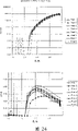
In blue emitter, F8 has the highest PL efficient in these materials.Therefore, it generally is elected to be the blue emission layer material in these materials.Fig. 4 is the strip-chart of the device of F8 for emission layer.Many (2,7-(9,9-two-n-octyl group fluorenes)-(1,4-penylene-(4-imino group (benzo acid))-1,4-penylene-(4-imino group (benzo acid))-1,4-penylene)) (" BFA ") layer is as the middle cavity transport layer.The substitute of BFA is PEDOT-PSS (be doped with poly styrene sulfonate to improve its conductive polyethylene dihydroxy benzenes, it can obtain for No. 970312.8 from Bayer AG and UK Patent Application), polyaniline, PVK etc.Hole transport layer also is used to block the passage of electronics to anode.II based semiconductor interface is arranged between BFA and F8.Fig. 5 illustrates the relation curve of device power efficiency and external efficiencies and driving voltage.Because the dark HOMO level (5.8eV) of F8 is corresponding to the corresponding energy level (4.8eV) among the ITO, therefore, device needs high driving voltage and low power efficiency is arranged, even the BFA intermediate layer is arranged.The about 0.03lm/W of power efficiency peak value, it is just in time under practical devices is acceptable.And because power efficiency is low, heating and the life-span that device can be serious short (approximately a few minutes).Even in the measurement phase to diagram data, find that device suffers rapid decay, believe be because of the heating recrystallization caused.This causes the skew of device emission spectrum, and with respect to the high-energy emission, the more low-yield emission of device increases.
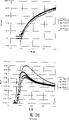
Fig. 6 is the strip-chart of second device, and wherein emission layer is 84%F8 mixing 16%PFM.The BFA layer is again as the middle cavity transport layer.Between BFA and F8, BFA and PFM and PFM and F8, II based semiconductor interface is arranged.Fig. 7 illustrates the relation curve of device power efficiency and external efficiencies and driving voltage.Compare with Fig. 5 device with Fig. 4, this peak device power efficient increases (0.33lm/W compares with 0.03lm/W), but does not reduce at the voltage of power efficiency peak value.This means that hole injection F8 main polymer (as the Figure 4 and 5 device) is positioned on the PFM section then in this device.Fig. 8 illustrates the device emission spectrum of comparing with F8 spectrum (line 11) (line 10).Fig. 8 points out on F8 enough combinations again take place, and means that the hole injects F8 from the BFA hole transport layer, but the major part that shows hole and electronics is again in conjunction with occurring in that PFM goes up rather than on F8.Thereby the hole of location forms electron-hole pair with rational probability, and electronic energy is excited to the PFM zone.This device peak value external efficiencies (see figure 7) is about 1Cd/A, and it is approximately than 10 times of Figure 4 and 5 devices.
Fig. 9 is the strip-chart of the 3rd device, and wherein emission layer is 84%F8 mixing 16%TFB.The BFA layer is again as the middle cavity transport layer.At least between BFA and F8 and TFB and F8, II based semiconductor interface is arranged.Figure 10 illustrates the relation curve of device power efficiency and external efficiencies and driving voltage.Compare with Fig. 5 device with Fig. 4, this device peak value external efficiencies has less increase (0.38Cd/A), and therefore littler peak power efficient (about 0.15lm/W) is arranged.Believe driving voltage reduce be because the corresponding energy level basically identical of the HOMO level of TFB and hole conveying material (BFA) this help the main body of hole injection light-emitting layer.Figure 11 illustrates the emission spectrum of device, and the emission of its display device, and penetrating property of the width of cloth combination again in device thus distribute between TFB and F8 polymer about equally.
Figure 12 is the strip-chart of four device, and wherein emission layer is 78%F8 mixing 15%TFB and 7%PFM.The BFA layer is again as the middle cavity transport layer.At least between BFA and F8, BFA and PFM, TFB and PFM, TFB and F8 and PFM and F8, II based semiconductor interface is arranged.Figure 13 illustrates the relation curve of device power efficiency and external efficiencies and driving voltage.This device is presented at significant improvement on the performance.The peak value external efficiencies is about 2.4Cd/A, and peak power efficient is about 1.05lm/W.Peak power efficient only takes place about 6.5V.Figure 14 illustrates the emission spectrum of device, and it shows that all emissions are from PFM.Following table is the comparison of these results and Fig. 4-11 device.
Table 2
| Emission layer is formed | Peak power efficient (lm/W) | Voltage during peak power efficient (V) | Peak value external efficiencies (Cd/A) | Emissive material |
| F8 | 0.03 | 8.7 | 0.074 | F8 |
| PFM∶F8 | 0.33 | 9.0 | 1 | PFM+F8 |
| TFB∶F8 | 0.15 | 7.0 | 0.37 | TFB+F8 |
| TFB∶PFM∶F8 | 1.05 | 6.5 | 2.4 | PFM |
The high efficiency of Figure 12-14 device is especially astonishing because its emission from as shown in table 1, in all materials useds the minimum PFM of PL efficient.
Believe that TFB is used for receiving the hole that enters the emission layer polymer body from hole transport layer in Figure 12-14 device, the hole then is positioned on the PFM section.Thereby TFB is used for promoting the hole to inject emission layer.The LUMO level of TFB roughly is half between the LUMO of F8 and PFM level, thus believe the LUMO level of TFB also provide when device strengthens electronics under bias voltage can rank in the middle of the transmission speed of PFM.And PFM has the optical energy gap than F8 or TFB summary tiny dots, and making it is favourable on energy for the exciton that forms on the PFM zone.
Can replace PFM with PFMO for Figure 12-14 device.The PL efficient of PFMO is that the power efficiency of 40% (seeing Table 1) resulting device when launching from PFMO is up to 1.5lm/W.Because PFMO has the optical energy gap identical with F8 and TFB (seeing Table 1), this result means that the Foster conversion is not a leading mechanism, and exciton is confined on the PFMO polymer thus, can strengthen efficient although observe it.And believe that under bias voltage, the energy adjustment between hole transport layer and TFB promotes the hole to inject the main body of emission layer.Be transported to the more low-energy HOMO level of PFMO subsequently.Yet when TFB existed, general half place also had LUMO energy rank between the LUMO of PFMO and F8 level.Thereby when device was subjected to bias voltage, TFB promoted electron transport on the PFMO polymer segments.May the energy level distortion arranged near the polymer interface place in actual applications, and not simple performance in Figure 12.
This explanation obtains negative electrode is changed to from LiAl result's that CaAl obtains support.The work function of CaAl is than the height of LiAl.If electronics transports and be activated to subsequently PFM or PFMO by F8 from the emission layer main body, so more the use of high work function material does not influence efficient, because also approach the LUMO level of F8.Yet if electronics also mainly is transported to PFM by TFB from LiAl cathode emission, power efficiency can reduce so, because need higher driving voltage overcome the obstacle of electronics emission between CaAl and the TFB.The applicant has observed between the device with LiAl or CaAl negative electrode does not have significant performance difference.
Figure 15 is the strip-chart of green emitted device, and wherein emission layer is another pair composition mixture of polymers.In this device, emission layer is 95%F8 mixing 5%F8BT.F8BT alloy and main body F8 form I based semiconductor interface, but two all form II based semiconductor interface with BFA.Figure 16 illustrates the power efficiency of device and the relation curve of external efficiencies and driving voltage.Power efficiency is for about about 2.0-2.5lm/W.Figure 17 illustrates the power efficiency of device and the relation curve of external efficiencies and driving voltage, this device is similar with 16 devices to Figure 15 but its emission layer is three constituents mixts: at first F8 and F8BT be with 19: 1 mixed, and this mixture and TFB are with 4: 1 mixed (that is: (F8: F8BT[0.95: 0.05]): TFB[0.75: 0.25 then]).Figure 18 is a kind of like this strip-chart of device.Figure 19 illustrates the power efficiency of device and the relation curve of external efficiencies and driving voltage, and this device but its emission layer similar with 16 devices to Figure 15 is (F8: F8BT[0.95: 0.05]): TFB[0.5: 0.5] mixture.The result of these three kinds of devices sums up in following table:
Table 3
| The amount of TFB (%) in the emission layer | Peak power efficient (lm/W) | Voltage during peak power efficient (V) | Peak value external efficiencies (Cd/A) | Voltage during the peak value external efficiencies (V) |
| 0 | 2.4 | 6.8 | 5.2 | About 8.5 |
| 25 | 6 | 3.8 | 8 | 4.5 |
| 50 | 6.7 | 3.5 | 7.8 | 3.8 |
When the amount of TFB reached between the 50%-60%, peak efficiencies reduced.External efficiencies also has increase when TFB increases, mainly in the 0-20%TFB scope.This is valuable to practical application.
Use 80: 20 structures of 5F8BT: TFB and PEDOT:PSS can realize efficient greater than 20lm/W as hole transport layer.(seeing Figure 22).
According to three above-mentioned composition blue emission mixtures, can believe that TFB promotes the hole to inject the polymer body of emission layer, and allow to form exciplex.In the green emitted device, exciplex has higher relatively probability to form exciton on F8BT, because higher fields inside is arranged and because can reduce energy (F8BT has the narrowest optical energy gap in main body) by the Foster conversion by doing them like this.This causes the raising of external efficiencies and power efficiency.
By comprise its one or more HOMO level (for example about 5.5eV) other polymer between TFB and F8 in emission layer, this device efficiency can further improve.This promotes hole to be activated to emission layer from TFB, and promotes the hole to be injected in himself emission layer main body in higher bias voltage field.
Should point out, in the green emitted mixture, comprise PFM and generally reduce device efficiency.Believe it is because its relative more shallow HOMO level, it is caught as the deep space cave rather than as intermediary, and thereby stops form exciton on the F8BT polymer.
Figure 20-27 illustrates some other embodiment of above-mentioned principle.
Emission layer is the mixture of F8BT, F8 and P PV in Figure 20.The F8BT:F8 mixture is coated in PPV and goes up and be used as the electron transport layer that allows electronics to transport between the conduction band in negative electrode and PPV.F8BT and F8 are added to PPV permission use than the more stable negative electrode of conventional AlLi negative electrode, even it has higher work function.In Figure 18, negative electrode is Mg, and its work function is 3.5eV.Substitute is Al, and its work function is 4.2eV.Can do further improvement by in mixture, comprising the terpolymer of its LUMO level between F8BT (3.4eV) and F8 (2.8eV).
In Figure 21, emission layer is the mixture of poly-(secondary penylene) (" PPP "), TFB and F8 and the CaAl negative electrode is arranged.The above-mentioned relevant principle of improving the hole injection also is suitable for to improve electronics at this device to be injected.
Figure 22 illustrate TFB join in the fluorenyl ejector system effect.Illustrating its emission layer among Figure 22 is brightness and the luminous intensity of device on the certain voltage scope of 5F8BT.Following among Figure 22 illustrates the equivalent data that its emission layer is the device of 5F8BT+20%TFB, and two devices all have the PEDOT:PSS hole transport layer.The result shows that increasing TFB brings up to about 20lm/W to peak efficiencies from about 3.5lm/W in emission layer.Have been found that PEDOT:PSS is better than BFA as hole transport layer in this kind device, especially when using " electron level " PEDOT:PSS.
It is not the data of the device of fluorenyl that Figure 23-25 illustrates its emission composition.Figure 23 illustrates the brightness (Cd/m of 8 pixels (" Fixel " refers to pixel among the figure) device on the certain voltage scope
2), current density (mA/cm
2), luminous efficiency (lm/W) and external efficiencies (Cd/A), wherein the emission layer of device is soluble PPV reflector Bis-DMOS PPV (two dimethyl-octa base silane polyphenylene vinylene, and two molecular formula are arranged on benzyl ring is SiMe
2C
8H
17Side unit, see Figure 27).Emission layer spins around the PEDOT:PSS hole transport layer.Figure 24 illustrates the equivalent data that its emission layer is the device of Bis-DMOS PPV+25%TFB.Finding to add TFB can be improved to threshold voltage about 2.5V and increase efficient to about 2.0lm/W from about 3.5V.Figure 25 illustrates a series of Devices Characteristics, wherein emission layer by another solubilized PPV (PPV A in the table 1) respectively with 0%, 2%, 10% or the 20%TFB additive form.Illustrate the current density of these devices and the relation curve of voltage among Figure 25.Illustrate the brightness of these devices and the relation curve of voltage among Figure 25.Following among Figure 25 illustrates the brightness of these devices when normal pressure 5.6V.Find that brightness and current density increase with TFB content.Under 5.6V voltage, add 20%TFB and find to increase by about 400% brightness than adding 0%TFB.
Figure 26 illustrates the brightness (Cd/m of 4 pixel devices on the certain voltage scope
2), current density (mA/cm
2), luminous efficiency (lm/W) and external efficiencies (Cd/A), wherein the emission layer of device is to have the polyvinyl polymer of TPD base side chain to form by 70%5F8BT and 30%.Maximal efficiency is 8lm/W, is 21lm/W but its emission layer has only the maximal efficiency of the device of 5F8BT.Figure 29 illustrates the periodicity voltammetry oxidation of the polyvinyl polymer of TPD base side chain and removes, and is illustrated in the 5.25eV zone i.e. HOMO level between emission composition and hole injection layer.
In some cases, the separation of surperficial phase to a certain degree wish to take place, and increase in the concentration near one or more composition of emission layer surface light-emitting layer, this is because the material interaction of emission layer and adjacently situated surfaces.Can use the atomic force microscope that comprises helical pattern or the method for other similar technique to detect this kind separation.
Figure 28 illustrates the brightness of a pair of device on the certain voltage scope, and wherein emission layer is formed by the mixture of the 5F8BT that is deposited on the PEDOT:PSS hole transport layer: TFB (4: 1).(line A) emission mixture directly is deposited on the PEDOT:PSS in a device.The TFB intermediate layer that (line B) is thin in another device directly is deposited on the PEDOT:PSS, launches mixture then and is deposited on the intermediate layer.Figure 28 illustrates, and the device with TFB intermediate layer shows that brightness has significant increase on fixed voltage.This believes it is because form the gradient of TFB constituent concentration in mixture, and this is since this composition to big than 5F8BT of the attraction in TFB intermediate layer.Because TFB can transport/catch composition as the hole in the mixture, be can be favourable so inject the promptly more close surface aggregation of side towards the emission layer hole with PEDOT:PSS for this composition.Injecting side from other the method for impelling this concentration gradient and electronics from any electron transport/catch composition towards emission layer produces similar concentration gradient and is expected to obtain similar result.
As the validity index in TFB intermediate layer, table 4 illustrates four kinds of devices peak value luminous efficiency at the trial.
Table 4
| Emission layer is formed | Is there there the TFB intermediate layer? | Peak value luminous efficiency (lm/W) |
| 5F8BT | Not | 6 |
| 5F8BT | Be | 8 |
| 5F8BT∶TFB(4∶1) | Not | 9 |
| 5F8BT∶TFB(4∶1) | Be | 12 |
The above-mentioned type multicomponent layer preferential deposition become individual layer.For realizing this point, the composition that constitutes this layer preferably before the deposit or among combine.This kind combination correspondingly comprises forming and comprises the material that this draws a little compositions, and for example, the molecule that contains more these compositions by formation by these compositions of physical mixed or (for example) together forms chemical mixture and carries out.
These compositions are by a chemically combined terpolymer that examples of materials is F8, F8BT and TFB, for example (5F8BT): TFB[80: 20].This kind material can form by the following method.In the 500mlr.b. arrow-necked bottle of being furnished with reflux condenser (linking to each other) and mechanical agitator, pack 9 into the nitrogen pipe, 9-dioctyl fluorene-2,7-hypoboric acid 1,2 ethylene glycol binary acid esters (4.773g, 9.0mmol), 2,7-dibromo benzothiadiazine (0.1504g, 0.51mmol), 2,7-two bromo-9,9-dioctyl fluorene (3.584g, 6.54mmol), N, N '-two-(4-bromine) phenyl-4-(butylidyne) aniline (0.8923g, 1.945mmol), 90ml toluene, tetrakis triphenylphosphine palladium (31.2mg) and 20ml 2mol sodium carbonate liquor.Stir the mixture rapidly, and reach 18 hours in 115 ℃ (oil sump temperature) heating.Add 100ml toluene and bromobenzene (1ml) again, and then under temperature (115 ℃ of oil sump temperature), stirred the mixture 3 hours.Then add phenylboric acid (1.5g) and under temperature, stirred the mixture 1 hour, then cool to room temperature.Reactant mixture is slowly poured into precipitation polymers in 41 methyl alcohol.But polymer deposit subsequently (for example from solution) forms the emission layer of light emitting devices.Generally speaking, an approach that forms suitable terpolymer is to allow provide the monomer of two kinds of compositions partly to react, and adding then provides ternary monomer and proceed polymerization.Copolymer can be any suitable form, for example at random, bulk or branch copolymer.
In the charge transport composition any adds glazing emission composition, and perhaps two transport composition and add glazing emission composition and can be combined in the individual molecule.Two compositions in conjunction with the time, form copolymer, and all three compositions in conjunction with the time can realize terpolymer.In the physical mixture of composition, may be because of being separated there be the tight mixing of composition, this can cause any or two invalid charge transports of launching composition to light from the charge transport composition.In the molecule in conjunction with charge transport composition and light emission composition, these unit are that chemistry connects, so compare with the physical mixture situation can be favourable for its charge transport.Contain the hole transport with the molecule of light emission composition can with electron transport material physical bond to generate effective light-emitting layer.In addition, contain electron transport and light the emission composition molecule can transport the material physical bond with the hole.If an electrode is especially effective, so effectively the LED structure can be made by ignoring to charge transport composition that should electrode and for emission layer uses two component molecules, and it comprises, and suitable opposite charges transports composition and light is launched composition.
But two composition chemical mixing of emission layer become individual molecule, and this material and the 3rd composition physical mixed that is provided by second molecule.
Above-mentioned device can be made with conventional method: polymeric layer from solution deposition to commercially available glass/ITO substrate, evaporation cathode deposit again.For example, the manufacturing of Figure 4 and 5 device is following to be described in detail: at first, by from N is arranged, N dimethyl formamide (" DMF ") as the solution spin-on deposition of 0.8% concentration of solvent to commercially available glass/ITO substrate.Polymeric layer ℃ is thirty minutes long by heating sample to 80 in nitrogen and dries.Emission layer obtains by being mixed with the solution spin coating of dimethylbenzene as 1.6% concentration of solvent then.The thickness targets of BFA layer and emission layer is respectively 10-80nm and 60-200nm; Typical thickness is respectively 65nm and 95nm.Deposit forms the thick Li layer of 20nm to last negative electrode by evaporation, forms the thick Al layer of 200nm subsequently.Device packs interior the encapsulation by being sealed in glass/epoxy in such as this inert atmosphere of nitrogen.
In the device that embodies above-mentioned principle, can use substitution material.For example, the substitution material of anode comprises tin-oxide (" TO ") and fluoridizes TO; The substitution material of hole transport layer comprises PEDOT: PSS and polyaniline; The substitution material of emission layer comprises PPV and MEH-PPV; The substitution material of negative electrode comprises Li, Ba, Mg, Ca, Ce, Cs, Eu, Rb, K, Sm, Na, Sm, Sr, Tb and Yb, the alloy of two or more these metals, one or more plant fluoride, carbide, oxide or the nitride of these metals, and one or more plant the alloy (for example LiAl) of the metal of these metals and one or more kind such as Al, Zr, Si, Sb, Sn, Zn, Mn, Ti, Cu, Co, W, Pb, In or Ag.Negative electrode can be transparent.Hole transport layer can be ignored, and the hole transport layer greater than perhaps can be arranged.Between negative electrode and emission layer one or more electron transport layer can be arranged, it helps electronics transporting and/or hinder the passage of hole to negative electrode from the negative electrode to the emission layer.
Hole transport layer can be a mixtures of material.For example, it can be the BFA that is mixed with the polymer of PFM etc., but the solution TDS for BFA that useful carboxylic acid group regulates.Any electron transport layer also can comprise the mixtures of material such as F8 and F8 BT.
Except efficient blueness and green emitted device were provided, above-mentioned principle can be used for more long wavelength's's (as ruddiness) ballistic device.Be starved of polymer because they have dark LUMO level for this device, this allows higher work function, more stable metal to be used for negative electrode and high PL efficient.Yet these polymer have dark HOMO level correspondingly.Although dark HOMO level is arranged but these polymer of above-mentioned principle permission use.
When manufacturing had the device of multicomponent emission layer, composition can correspondingly mix before deposit.Yet, for the electronics effect optimization that makes composition so that utilize above-mentioned principle, the composition of preferred emission layer is part or all of phase-separation, and therefore the diffusion zone (see United States Patent (USP) 5760791, its content is hereby incorporated by reference) of every kind of composition is arranged in emission layer.When the needs charge carrier from a kind of composition when another kind moves, the structure of mixed layer (the especially size of the characteristic of these compositions and every kind of composition range) should preferably provide enough interfaces between these compositions.The zone of every kind of composition can be by layer diffusion equably, and perhaps accumulating in for one or more plant compositions is favourable near one between light-emitting layer and the carrier injection layer or other at the interface.Can find that it is desirable in the more close anode-side of emission layer the hole-injecting material (littler near cathode side concentration) of bigger concentration being arranged.Can find that it is desirable at the more close cathode side of emission layer the electronics injection material (littler near anode-side concentration) of bigger concentration being arranged.
Diffusion property (comprising the distribution of various compositions in layer) for influencing mixed layer can adopt some technology.Surface between one or more kind compositions and other layer of device (especially emission layer is deposited to the layer on it) reacts to each other and can be used, and promotes being separated in emission layer to a certain extent.Preferably, deposition conditions is arranged to such an extent that make suitable in hole conveying material or the electron transport material one preferentially to be launched the layer of layer deposit on it and to attract or repel.Thereby, if being deposited on the hole, injects on the anode layer emission layer, so preferred hole-injecting material preferentially is attracted to this surface and/or electronics injection material preferentially by this exclusion., injects on the cathode layer emission layer so preferred opposite application if being deposited on electronics.Emission layer wants the material on the surface of deposit on it can handle or select to obtain this preferential effect.When two or more compositions of emission layer composition were combined in the identical molecule, the mode of their combinations can be used to promote be separated (or segregation) state or the uniformity of needs.For example, in conjunction with molecule can be combined into suitable at random, the polymer of bulk or branch-like to be to reach required effect.Comprise solvent (as chloroform or dimethylbenzene), solvent evaporation pressure, molecular wt, composition surface energy (surface each other and/or emission layer will be deposited to the Free Surface on it), polydispersity, composition volume factor, architectural feature of use etc. with the relevant other factors that is separated.
Any feature or combination of features or their summary that the present invention can comprise herein impliedly or discuss clearly, and no matter whether relate to claims of the present invention.Obviously, in conjunction with the description of front, those skilled in the art can make various changes within the scope of the present invention.
Claims (24)
1. an electroluminescent device is characterized in that, comprising:
Be used to inject first carrier injection layer of positive carrier;
Be used to inject second carrier injection layer of negative carrier; With
Light-emitting layer between described first and second carrier injection layer, this light-emitting layer comprises following mixture of ingredients:
Be used for receiving first composition of positive carrier from first carrier injection layer;
Be used for receiving second composition of negative carrier from second carrier injection layer; With
To combine from the charge carrier of first and second compositions and produce the 3rd organic light emission composition of light;
At least two compositions are combined into individual molecule among described first, second and the 3rd composition,
Another composition among at least one composition among described first, second and the 3rd composition and described first, second and the 3rd composition forms II based semiconductor interface.
2. electroluminescent device according to claim 1 is characterized in that, described first, second is combined into single polymer with the 3rd composition.
3. electroluminescent device according to claim 2 is characterized in that, described the 3rd composition is the side group of the first and/or second composition polymer chain.
4. electroluminescent device according to claim 2 is characterized in that, described first and/or second composition is one or more a side group of the 3rd composition polymer chain.
5. electroluminescent device according to claim 1 is characterized in that, the arbitrary composition among described first, second and the 3rd composition all and described first, second and the 3rd composition forms II based semiconductor interface.
6. electroluminescent device according to claim 1 is characterized in that described ternary optical energy gap is greater than 1.8eV.
7. electroluminescent device according to claim 1 is characterized in that, described first composition can receive from the positive carrier of described first carrier injection layer and comprise in main chain and/or as the conjugated polymer of the amido of side group.
8. electroluminescent device according to claim 1 is characterized in that, second composition is many (2,7-9,9-two-n-octyl group fluorenes).
9. electroluminescent device according to claim 1 is characterized in that, described first composition have described second and ternary lowest unoccupied molecular orbital energy level between the lowest unoccupied molecular orbital energy level.
10. electroluminescent device according to claim 1 is characterized in that, described the 3rd composition is many (2,7-(9,9-two-n-octyl group fluorenes)-(1,4-penylene-((4-aminomethyl phenyl) imino group) 1,4-penylene-((4-aminomethyl phenyl) imino group)-1, the 4-penylene)).
11. electroluminescent device according to claim 1 is characterized in that, described ternary optical energy gap is less than the optical energy gap of first and second compositions.
12. electroluminescent device according to claim 1 is characterized in that, described the 3rd composition is many ((2,7-(9,9)-two-n-octyl group fluorenes)-3,6-benzothiadiazines) or soluble poly (phenylenevinylene).
13. electroluminescent device according to claim 1 is characterized in that, described first, second and the ternary at least one be organic material.
14. electroluminescent device according to claim 2 is characterized in that, described polymer is a conjugated polymer.
15. electroluminescent device according to claim 1 is characterized in that, described first carrier injection layer is the positive carrier transport layer between described light-emitting layer and anode electrode layer.
16. electroluminescent device according to claim 15 is characterized in that, described first carrier injection layer and light-emitting layer form II based semiconductor interface.
17. electroluminescent device according to claim 1 is characterized in that, described first carrier injection layer is an anode electrode layer.
18. electroluminescent device according to claim 15 is characterized in that, the work function of described anode electrode layer is greater than 4.3eV.
19. electroluminescent device according to claim 1 is characterized in that, described second carrier injection layer is the negative carrier transport layer between light-emitting layer and negative electrode layer.
20. electroluminescent device according to claim 19 is characterized in that, described second carrier injection layer and light-emitting layer form II based semiconductor interface.
21. electroluminescent device according to claim 1 is characterized in that, described second carrier injection layer is a negative electrode layer.
22. electroluminescent device according to claim 19 is characterized in that, the work function of described negative electrode layer is less than 3.5eV.
23. electroluminescent device according to claim 15 is characterized in that, described anode electrode layer is a transmitted light.
24. electroluminescent device according to claim 19 is characterized in that, described negative electrode layer is a transmitted light.
Applications Claiming Priority (2)
| Application Number | Priority Date | Filing Date | Title |
|---|---|---|---|
| GBGB9805476.0A GB9805476D0 (en) | 1998-03-13 | 1998-03-13 | Electroluminescent devices |
| GB9805476.0 | 1998-03-13 |
Related Child Applications (4)
| Application Number | Title | Priority Date | Filing Date |
|---|---|---|---|
| CN2007101437398A Division CN101136455B (en) | 1998-03-13 | 1999-03-12 | Electroluminescent devices |
| CN2007101290957A Division CN101106182B (en) | 1998-03-13 | 1999-03-12 | Electroluminescent devices |
| CN200610071989A Division CN100576601C (en) | 1998-03-13 | 1999-03-12 | Electroluminescent device |
| CN200710143738A Division CN100589259C (en) | 1998-03-13 | 1999-03-12 | Electroluminescent devices |
Publications (2)
| Publication Number | Publication Date |
|---|---|
| CN1293826A CN1293826A (en) | 2001-05-02 |
| CN1331247C true CN1331247C (en) | 2007-08-08 |
Family
ID=10828566
Family Applications (5)
| Application Number | Title | Priority Date | Filing Date |
|---|---|---|---|
| CNB998039810A Expired - Lifetime CN1331247C (en) | 1998-03-13 | 1999-03-12 | Electroluminescent devices |
| CN200710143738A Expired - Lifetime CN100589259C (en) | 1998-03-13 | 1999-03-12 | Electroluminescent devices |
| CN2007101437398A Expired - Lifetime CN101136455B (en) | 1998-03-13 | 1999-03-12 | Electroluminescent devices |
| CN200610071989A Expired - Lifetime CN100576601C (en) | 1998-03-13 | 1999-03-12 | Electroluminescent device |
| CN2007101290957A Expired - Lifetime CN101106182B (en) | 1998-03-13 | 1999-03-12 | Electroluminescent devices |
Family Applications After (4)
| Application Number | Title | Priority Date | Filing Date |
|---|---|---|---|
| CN200710143738A Expired - Lifetime CN100589259C (en) | 1998-03-13 | 1999-03-12 | Electroluminescent devices |
| CN2007101437398A Expired - Lifetime CN101136455B (en) | 1998-03-13 | 1999-03-12 | Electroluminescent devices |
| CN200610071989A Expired - Lifetime CN100576601C (en) | 1998-03-13 | 1999-03-12 | Electroluminescent device |
| CN2007101290957A Expired - Lifetime CN101106182B (en) | 1998-03-13 | 1999-03-12 | Electroluminescent devices |
Country Status (11)
| Country | Link |
|---|---|
| US (6) | US6897473B1 (en) |
| EP (5) | EP1062703B1 (en) |
| JP (5) | JP2002507825A (en) |
| KR (6) | KR20070044034A (en) |
| CN (5) | CN1331247C (en) |
| AU (1) | AU2740299A (en) |
| DE (1) | DE69939815D1 (en) |
| GB (1) | GB9805476D0 (en) |
| HK (1) | HK1098577A1 (en) |
| TW (1) | TW525409B (en) |
| WO (1) | WO1999048160A1 (en) |
Families Citing this family (233)
| Publication number | Priority date | Publication date | Assignee | Title |
|---|---|---|---|---|
| US6309763B1 (en) * | 1997-05-21 | 2001-10-30 | The Dow Chemical Company | Fluorene-containing polymers and electroluminescent devices therefrom |
| KR100697861B1 (en) * | 1998-03-13 | 2007-03-22 | 캠브리지 디스플레이 테크놀로지 리미티드 | Electroluminescent devices |
| GB9805476D0 (en) * | 1998-03-13 | 1998-05-13 | Cambridge Display Tech Ltd | Electroluminescent devices |
| DE19846768A1 (en) * | 1998-10-10 | 2000-04-20 | Aventis Res & Tech Gmbh & Co | A conjugated polymer useful as an organic semiconductor, an electroluminescence material, and for display elements in television monitor and illumination technology contains fluorene building units |
| CN1206254C (en) * | 1999-02-04 | 2005-06-15 | 陶氏环球技术公司 | Fluorene copolymers and devices made therefrom |
| EP2267814A1 (en) * | 1999-03-12 | 2010-12-29 | Sumitomo Chemical Company, Limited | Polymers, their preparation and uses |
| WO2001026425A1 (en) * | 1999-10-05 | 2001-04-12 | Matsushita Electric Industrial Co., Ltd. | Luminescent device and method for manufacturing the same, and display and illuminator comprising the same |
| DE60121611T2 (en) | 2000-09-26 | 2007-07-26 | Cambridge Display Technology Ltd. | Twisted polymers, their use and methods of making random copopymeres |
| DE60125202T2 (en) * | 2000-09-26 | 2007-11-08 | Cambridge Display Technology Ltd. | POLYMERS AND ITS USES |
| WO2002028983A1 (en) * | 2000-10-03 | 2002-04-11 | Cambridge Display Techbnology Limited | Light-emissive polymer blends and light-emissive devices made from the same |
| US6803720B2 (en) * | 2000-12-15 | 2004-10-12 | Universal Display Corporation | Highly stable and efficient OLEDs with a phosphorescent-doped mixed layer architecture |
| WO2002059121A1 (en) | 2001-01-24 | 2002-08-01 | Cambridge Display Technology Limited | Monomer for use in preparation of a polymer to be used in optical devices |
| GB0109108D0 (en) | 2001-04-11 | 2001-05-30 | Cambridge Display Tech Ltd | Polymer, its preparation and uses |
| GB0109295D0 (en) * | 2001-04-12 | 2001-05-30 | Univ Cambridge Tech | Optoelectronic devices and a method for producing the same |
| US7632908B2 (en) | 2001-05-11 | 2009-12-15 | Cambridge Display Technology Limited | Substituted fluorene polymers, their preparation and use in optical devices |
| WO2002095841A2 (en) | 2001-05-18 | 2002-11-28 | Cambridge University Technical Services Limited | Electroluminescent device |
| WO2003000773A1 (en) * | 2001-06-22 | 2003-01-03 | Cambridge Display Technology Limited | Polymer containing substituted triphenylamine units |
| DE60229850D1 (en) | 2001-07-10 | 2008-12-24 | Dow Global Technologies Inc | ELECTROACTIVE POLYMERS AND DEVICES MANUFACTURED THEREFROM |
| GB2379317A (en) | 2001-08-30 | 2003-03-05 | Cambridge Display Tech Ltd | Optoelectronic display operating by photoluminescence quenching |
| GB0125620D0 (en) | 2001-10-25 | 2001-12-19 | Cambridge Display Tech Ltd | Monomers and low band gap polymers formed therefrom |
| GB2381643A (en) | 2001-10-31 | 2003-05-07 | Cambridge Display Tech Ltd | Display drivers |
| GB2381644A (en) | 2001-10-31 | 2003-05-07 | Cambridge Display Tech Ltd | Display drivers |
| GB2386462A (en) | 2002-03-14 | 2003-09-17 | Cambridge Display Tech Ltd | Display driver circuits |
| SG128438A1 (en) | 2002-03-15 | 2007-01-30 | Sumitomo Chemical Co | Polymer compound and polymer light emitting deviceusing the same |
| GB0209502D0 (en) | 2002-04-25 | 2002-06-05 | Cambridge Display Tech Ltd | Display driver circuits |
| GB2388236A (en) | 2002-05-01 | 2003-11-05 | Cambridge Display Tech Ltd | Display and driver circuits |
| CN1325600C (en) | 2002-05-10 | 2007-07-11 | 剑桥显示技术有限公司 | Polymers their preparation and uses |
| DE10224021B4 (en) | 2002-05-24 | 2006-06-01 | Novaled Gmbh | Phosphorescent light emitting device with organic layers |
| GB2389951A (en) | 2002-06-18 | 2003-12-24 | Cambridge Display Tech Ltd | Display driver circuits for active matrix OLED displays |
| GB2389952A (en) | 2002-06-18 | 2003-12-24 | Cambridge Display Tech Ltd | Driver circuits for electroluminescent displays with reduced power consumption |
| SG119187A1 (en) * | 2002-06-28 | 2006-02-28 | Semiconductor Energy Lab | Light emitting device and manufacturing method therefor |
| US7074534B2 (en) | 2002-07-10 | 2006-07-11 | E. I. Du Pont De Nemours And Company | Polymeric charge transport compositions and electronic devices made with such compositions |
| WO2004009668A1 (en) * | 2002-07-22 | 2004-01-29 | Sumitomo Chemical Company, Limited | Copolymer and polymeric luminescent element comprising the same |
| WO2004023573A2 (en) * | 2002-09-03 | 2004-03-18 | Cambridge Display Technology Limited | Optical device |
| EP1571170B1 (en) | 2002-10-30 | 2018-09-05 | Sumitomo Chemical Company, Limited | High-molecular compounds and polymer light emitting devices made by using the same |
| GB0225869D0 (en) | 2002-11-06 | 2002-12-11 | Cambridge Display Tech Ltd | Polymer |
| GB0226010D0 (en) | 2002-11-08 | 2002-12-18 | Cambridge Display Tech Ltd | Polymers for use in organic electroluminescent devices |
| JP4152173B2 (en) * | 2002-11-18 | 2008-09-17 | 出光興産株式会社 | Organic electroluminescence device |
| GB0227778D0 (en) | 2002-11-28 | 2003-01-08 | Cambridge Display Tech Ltd | Droplet-deposition related methods and apparatus |
| US6916902B2 (en) * | 2002-12-19 | 2005-07-12 | Dow Global Technologies Inc. | Tricyclic arylamine containing polymers and electronic devices therefrom |
| GB0300105D0 (en) * | 2003-01-03 | 2003-02-05 | Cambridge Display Tech Ltd | Ablation methods & apparatus |
| GB0306414D0 (en) * | 2003-03-20 | 2003-04-23 | Cambridge Display Tech Ltd | Polymers,their preparations and uses |
| GB0306409D0 (en) | 2003-03-20 | 2003-04-23 | Cambridge Display Tech Ltd | Electroluminescent device |
| JP2007504342A (en) | 2003-05-30 | 2007-03-01 | メルク パテント ゲーエムベーハー | polymer |
| EP1491568A1 (en) | 2003-06-23 | 2004-12-29 | Covion Organic Semiconductors GmbH | Semiconductive Polymers |
| US20050019607A1 (en) * | 2003-06-30 | 2005-01-27 | Franky So | OLED device with mixed emissive layer |
| GB0321781D0 (en) | 2003-09-17 | 2003-10-15 | Toppan Printing Company Ltd | Electroluminescent device |
| US20050069727A1 (en) * | 2003-09-30 | 2005-03-31 | Rahul Gupta | Oled emissive polymer layer |
| ES2387304T3 (en) | 2003-10-28 | 2012-09-20 | Basf Se | New dicetopyrrolopyrrole polymers |
| JP4390113B2 (en) | 2003-11-10 | 2009-12-24 | ケンブリッジ ディスプレイ テクノロジー リミテッド | Dibenzosilol polymer and method for producing the same |
| GB0326853D0 (en) * | 2003-11-19 | 2003-12-24 | Cambridge Display Tech Ltd | Optical device |
| CN100558791C (en) * | 2003-12-13 | 2009-11-11 | 默克专利有限公司 | Oligopolymer and polymkeric substance |
| GB0329364D0 (en) * | 2003-12-19 | 2004-01-21 | Cambridge Display Tech Ltd | Optical device |
| GB0401613D0 (en) | 2004-01-26 | 2004-02-25 | Cambridge Display Tech Ltd | Organic light emitting diode |
| GB2410600A (en) | 2004-01-30 | 2005-08-03 | Cambridge Display Tech Ltd | Organic light emitting diode display device |
| JP5092199B2 (en) * | 2004-02-02 | 2012-12-05 | 住友化学株式会社 | Organic electroluminescence device |
| TWI270318B (en) * | 2004-03-30 | 2007-01-01 | Osram Opto Semiconductors Gmbh | Device structure to improve OLED reliability |
| US7737632B2 (en) * | 2004-04-27 | 2010-06-15 | Fujifilm Corporation | Organic EL element with lamination structure and its manufacturing method |
| GB2447637B (en) | 2004-08-04 | 2009-11-18 | Cambridge Display Tech Ltd | Organic Electroluminescent Device |
| US7540978B2 (en) | 2004-08-05 | 2009-06-02 | Novaled Ag | Use of an organic matrix material for producing an organic semiconductor material, organic semiconductor material and electronic component |
| EP1627891A1 (en) | 2004-08-11 | 2006-02-22 | Covion Organic Semiconductors GmbH | Polymers for use in organic electroluminescent devices |
| KR101027896B1 (en) | 2004-08-13 | 2011-04-07 | 테크니셰 유니베르시테트 드레스덴 | Layer assembly for a light-emitting component |
| JP4238194B2 (en) * | 2004-09-17 | 2009-03-11 | セイコーエプソン株式会社 | ORGANIC ELECTROLUMINESCENT DEVICE, METHOD FOR PRODUCING ORGANIC ELECTROLUMINESCENT DEVICE, ELECTRONIC DEVICE |
| JP4916102B2 (en) * | 2004-09-24 | 2012-04-11 | シャープ株式会社 | Organic EL device |
| GB0421711D0 (en) * | 2004-09-30 | 2004-11-03 | Cambridge Display Tech Ltd | Multi-line addressing methods and apparatus |
| GB0421712D0 (en) | 2004-09-30 | 2004-11-03 | Cambridge Display Tech Ltd | Multi-line addressing methods and apparatus |
| BRPI0516867A (en) * | 2004-09-30 | 2008-09-23 | Cambridge Display Tech Ltd | Multiple line addressing methods and apparatus |
| GB0428191D0 (en) | 2004-12-23 | 2005-01-26 | Cambridge Display Tech Ltd | Digital signal processing methods and apparatus |
| GB0421710D0 (en) | 2004-09-30 | 2004-11-03 | Cambridge Display Tech Ltd | Multi-line addressing methods and apparatus |
| EP1648042B1 (en) | 2004-10-07 | 2007-05-02 | Novaled AG | A method for doping a semiconductor material with cesium |
| GB2433512B (en) | 2004-10-11 | 2009-06-03 | Cambridge Display Tech Ltd | Polar semiconductive hole transporting material |
| JP4653469B2 (en) | 2004-12-01 | 2011-03-16 | 出光興産株式会社 | Organic electroluminescence device |
| GB0427965D0 (en) | 2004-12-22 | 2005-01-26 | Cambridge Display Technology O | Process for the synthesis of arylfluorenes and analogues thereof |
| ATE555506T1 (en) | 2004-12-24 | 2012-05-15 | Cdt Oxford Ltd | LIGHT EMITTING DEVICE |
| GB0428445D0 (en) | 2004-12-29 | 2005-02-02 | Cambridge Display Tech Ltd | Blue-shifted triarylamine polymer |
| GB0428444D0 (en) | 2004-12-29 | 2005-02-02 | Cambridge Display Tech Ltd | Conductive polymer compositions in opto-electrical devices |
| JP2008525608A (en) | 2004-12-29 | 2008-07-17 | ケンブリッジ ディスプレイ テクノロジー リミテッド | Hard amine |
| KR101074786B1 (en) * | 2004-12-31 | 2011-10-19 | 삼성모바일디스플레이주식회사 | Organic electroluminescence device comprising electron blocking layer comprising polyimide containing triphenylamine derivative structure |
| JP4450207B2 (en) * | 2005-01-14 | 2010-04-14 | セイコーエプソン株式会社 | Method for manufacturing light emitting device |
| DE502005002342D1 (en) * | 2005-03-15 | 2008-02-07 | Novaled Ag | Light-emitting component |
| US7683536B2 (en) * | 2005-03-31 | 2010-03-23 | The Trustees Of Princeton University | OLEDs utilizing direct injection to the triplet state |
| EP2284923B1 (en) | 2005-04-13 | 2016-12-28 | Novaled GmbH | Assembly for an organic pin-type LED and manufacturing method |
| GB0507684D0 (en) | 2005-04-15 | 2005-05-25 | Cambridge Display Tech Ltd | Pulsed driven displays |
| GB0510382D0 (en) | 2005-05-20 | 2005-06-29 | Cambridge Display Tech Ltd | Ink jet printing compositions in opto-electrical devices |
| EP1727221B1 (en) * | 2005-05-27 | 2010-04-14 | Novaled AG | Transparent organic light emitting diode |
| JP5119611B2 (en) * | 2005-06-01 | 2013-01-16 | 住友化学株式会社 | Polymer composition and polymer light emitting device |
| EP1729346A1 (en) * | 2005-06-01 | 2006-12-06 | Novaled AG | Light-emitting device with an electrode arrangement |
| EP1739765A1 (en) * | 2005-07-01 | 2007-01-03 | Novaled AG | Organic light-emitting diode and stack of organic light emitting diodes |
| GB0514476D0 (en) * | 2005-07-14 | 2005-08-17 | Cambridge Display Tech Ltd | Conductive polymer compositions in opto-electrical devices |
| TW200718726A (en) | 2005-08-12 | 2007-05-16 | Sumitomo Chemical Co | Polymer and polymer light-emitting element using the same |
| DE112006002220B4 (en) | 2005-08-23 | 2018-05-24 | Cambridge Display Technology Ltd. | Organic electronic device structures and manufacturing processes |
| GB0517195D0 (en) | 2005-08-23 | 2005-09-28 | Cambridge Display Tech Ltd | Molecular electronic device structures and fabrication methods |
| KR101193179B1 (en) * | 2005-08-26 | 2012-10-19 | 삼성디스플레이 주식회사 | Organosiloxane compound and organic electroluminescence device comprsing the same |
| GB2430069A (en) | 2005-09-12 | 2007-03-14 | Cambridge Display Tech Ltd | Active matrix display drive control systems |
| GB0518968D0 (en) | 2005-09-16 | 2005-10-26 | Cdt Oxford Ltd | Organic light-emitting device |
| DE112006002668T5 (en) | 2005-10-07 | 2008-08-14 | Sumitomo Chemical Company, Ltd. | Copolymer and polymeric light-emitting device using the same |
| GB2431276B (en) | 2005-10-14 | 2008-11-12 | Cambridge Display Tech Ltd | Display monitoring systems |
| CN101356211A (en) | 2005-11-11 | 2009-01-28 | 住友化学株式会社 | Conjugated polymeric compound and polymeric electroluminescence element using the same |
| KR101193180B1 (en) * | 2005-11-14 | 2012-10-19 | 삼성디스플레이 주식회사 | A conducting polymer composition and an electronic device employing the layer obtained from the conducting polymer composition |
| DE112006002998T5 (en) | 2005-11-18 | 2008-09-18 | Sumitomo Chemical Co., Ltd. | Polymer compound and polymer-containing light-emitting device using the same |
| KR101243917B1 (en) * | 2005-12-19 | 2013-03-14 | 삼성디스플레이 주식회사 | A conducting polymer composition and an electrical device employing the layer obtained from the conducting polymer composition |
| EP1806795B1 (en) | 2005-12-21 | 2008-07-09 | Novaled AG | Organic Device |
| GB0526185D0 (en) | 2005-12-22 | 2006-02-01 | Cambridge Display Tech Ltd | Electronic device |
| GB2433638B (en) | 2005-12-22 | 2011-06-29 | Cambridge Display Tech Ltd | Passive matrix display drivers |
| GB2433509A (en) | 2005-12-22 | 2007-06-27 | Cambridge Display Tech Ltd | Arylamine polymer |
| EP1804308B1 (en) * | 2005-12-23 | 2012-04-04 | Novaled AG | An organic light emitting device with a plurality of organic electroluminescent units stacked upon each other |
| DE602006001930D1 (en) * | 2005-12-23 | 2008-09-04 | Novaled Ag | of organic layers |
| GB0526393D0 (en) | 2005-12-23 | 2006-02-08 | Cdt Oxford Ltd | Light emissive device |
| CN101389685A (en) | 2005-12-28 | 2009-03-18 | 住友化学株式会社 | Block copolymer |
| EP1808909A1 (en) | 2006-01-11 | 2007-07-18 | Novaled AG | Electroluminescent light-emitting device |
| US7968904B2 (en) * | 2006-02-06 | 2011-06-28 | Fujifilm Corporation | Organic electroluminescence device |
| JP2007220772A (en) * | 2006-02-15 | 2007-08-30 | Idemitsu Kosan Co Ltd | Polymer compound for organic electroluminescence element and its manufacturing method |
| GB2437113B (en) | 2006-04-12 | 2008-11-26 | Cambridge Display Tech Ltd | Light-emissive display and method of manufacturing the same |
| KR20070101984A (en) * | 2006-04-13 | 2007-10-18 | 삼성에스디아이 주식회사 | Organic electroluminescent device comprising charge separation layer |
| EP1848049B1 (en) * | 2006-04-19 | 2009-12-09 | Novaled AG | Light emitting device |
| GB2440934B (en) | 2006-04-28 | 2009-12-16 | Cdt Oxford Ltd | Opto-electrical polymers and devices |
| US20070275265A1 (en) * | 2006-05-25 | 2007-11-29 | Au Optronics Corporation | Organic light emitting layer with a reduced phosphorescent dopant concentration and applications of same |
| GB2439358B (en) | 2006-06-19 | 2010-12-15 | Cambridge Display Tech Ltd | Organic electroluminescent optocouplers |
| JP5461181B2 (en) * | 2006-07-25 | 2014-04-02 | メルク パテント ゲーエムベーハー | Polymer blends and their use in organic light-emitting devices |
| ES2554800T3 (en) | 2006-07-28 | 2015-12-23 | Basf Se | Novel polymers |
| US20090263567A1 (en) | 2006-08-01 | 2009-10-22 | Cambridge Display Technology Limited | Methods of Manufacturing Opto-Electrical Devices |
| TW200818981A (en) | 2006-08-30 | 2008-04-16 | Sumitomo Chemical Co | Organic electroluminescence device |
| GB0617167D0 (en) | 2006-08-31 | 2006-10-11 | Cdt Oxford Ltd | Compounds for use in opto-electrical devices |
| GB2441354B (en) | 2006-08-31 | 2009-07-29 | Cambridge Display Tech Ltd | Display drive systems |
| GB2455215B (en) | 2006-08-31 | 2009-09-30 | Cambridge Display Tech Ltd | Method for fabricating an organic electronic device |
| US20100038658A1 (en) * | 2006-09-11 | 2010-02-18 | Vanderbilt University | Polymer light-emitting diode and fabrication of same by resonant infrared laser vapor deposition |
| JP2008098619A (en) * | 2006-09-14 | 2008-04-24 | Sumitomo Chemical Co Ltd | Organic electroluminescent device |
| WO2008032843A1 (en) | 2006-09-14 | 2008-03-20 | Sumitomo Chemical Company, Limited | Organic electroluminescent device |
| GB0618698D0 (en) | 2006-09-22 | 2006-11-01 | Cambridge Display Tech Ltd | Molecular electronic device fabrication methods and structures |
| WO2008038814A1 (en) * | 2006-09-26 | 2008-04-03 | Sumitomo Chemical Company, Limited | Polymeric adsorption films and processes for producing these |
| GB0620045D0 (en) | 2006-10-10 | 2006-11-22 | Cdt Oxford Ltd | Otpo-electrical devices and methods of making the same |
| DE102006059509B4 (en) * | 2006-12-14 | 2012-05-03 | Novaled Ag | Organic light-emitting element |
| GB2448175B (en) | 2007-04-04 | 2009-07-22 | Cambridge Display Tech Ltd | Thin film transistor |
| DE102007019260B4 (en) * | 2007-04-17 | 2020-01-16 | Novaled Gmbh | Non-volatile organic storage element |
| JP5374908B2 (en) | 2007-04-27 | 2013-12-25 | 住友化学株式会社 | Pyrene polymer compound and light emitting device using the same |
| JP5248910B2 (en) | 2007-05-30 | 2013-07-31 | 住友化学株式会社 | ORGANIC ELECTROLUMINESCENT ELEMENT AND DISPLAY DEVICE USING THE ELEMENT |
| JP2009021104A (en) | 2007-07-12 | 2009-01-29 | Sumitomo Chemical Co Ltd | Manufacturing method for organic light emitting element |
| GB2453375A (en) | 2007-10-05 | 2009-04-08 | Cambridge Display Tech Ltd | Driving a display using an effective analogue drive signal generated from a modulated digital signal |
| GB2453374A (en) | 2007-10-05 | 2009-04-08 | Cambridge Display Tech Ltd | Matching multiple current sources/sinks |
| GB0721567D0 (en) | 2007-11-02 | 2007-12-12 | Cambridge Display Tech Ltd | Pixel driver circuits |
| GB2454867B (en) | 2007-11-09 | 2010-02-03 | Cambridge Display Tech Ltd | Electroluminescent devices comprising bus bar |
| GB2454890B (en) | 2007-11-21 | 2010-08-25 | Limited Cambridge Display Technology | Light-emitting device and materials therefor |
| JP5217931B2 (en) | 2007-11-29 | 2013-06-19 | 住友化学株式会社 | Organic electroluminescence device and method for manufacturing the same |
| GB2455747B (en) | 2007-12-19 | 2011-02-09 | Cambridge Display Tech Ltd | Electronic devices and methods of making the same using solution processing techniques |
| KR20100106426A (en) | 2007-12-28 | 2010-10-01 | 스미또모 가가꾸 가부시키가이샤 | Polymer light-emitting device, method for manufacturing the same and polymer light-emitting display device |
| GB2456788B (en) | 2008-01-23 | 2011-03-09 | Cambridge Display Tech Ltd | White light emitting material |
| GB0803950D0 (en) | 2008-03-03 | 2008-04-09 | Cambridge Display Technology O | Solvent for printing composition |
| TWI496689B (en) | 2008-03-07 | 2015-08-21 | Sumitomo Chemical Co | Laminatyed construction |
| GB2458454B (en) | 2008-03-14 | 2011-03-16 | Cambridge Display Tech Ltd | Electronic devices and methods of making the same using solution processing techniques |
| GB2460018B (en) | 2008-05-07 | 2013-01-30 | Cambridge Display Tech Ltd | Active matrix displays |
| GB2459895B (en) | 2008-05-09 | 2011-04-27 | Cambridge Display Technology Limited | Organic light emissive device |
| GB2462410B (en) | 2008-07-21 | 2011-04-27 | Cambridge Display Tech Ltd | Compositions and methods for manufacturing light-emissive devices |
| GB2462122B (en) | 2008-07-25 | 2013-04-03 | Cambridge Display Tech Ltd | Electroluminescent materials |
| WO2010013725A1 (en) | 2008-07-30 | 2010-02-04 | 住友化学株式会社 | Laminated structure, method for producing same, and electronic element comprising same |
| GB2462314B (en) | 2008-08-01 | 2011-03-16 | Cambridge Display Tech Ltd | Organic light-emiting materials and devices |
| GB0814161D0 (en) | 2008-08-01 | 2008-09-10 | Cambridge Display Tech Ltd | Blue-light emitting material |
| GB2462296A (en) | 2008-08-01 | 2010-02-03 | Cambridge Display Tech Ltd | Pixel driver circuits |
| DE102008036063B4 (en) * | 2008-08-04 | 2017-08-31 | Novaled Gmbh | Organic field effect transistor |
| DE102008036062B4 (en) | 2008-08-04 | 2015-11-12 | Novaled Ag | Organic field effect transistor |
| GB2462646B (en) | 2008-08-15 | 2011-05-11 | Cambridge Display Tech Ltd | Active matrix displays |
| GB0814971D0 (en) | 2008-08-15 | 2008-09-24 | Cambridge Display Tech Ltd | Opto-electrical devices and methods of manufacturing the same |
| GB2462844B (en) | 2008-08-21 | 2011-04-20 | Cambridge Display Tech Ltd | Organic electroluminescent device |
| GB2462688B (en) | 2008-08-22 | 2012-03-07 | Cambridge Display Tech Ltd | Opto-electrical devices and methods of manufacturing the same |
| GB2463040B (en) | 2008-08-28 | 2012-10-31 | Cambridge Display Tech Ltd | Light-emitting material |
| GB2463077B (en) | 2008-09-02 | 2012-11-07 | Sumitomo Chemical Co | Electroluminescent material and device |
| GB2463493B (en) | 2008-09-15 | 2012-11-14 | Cambridge Display Tech Ltd | An improved method for ink jet printing organic electronic devices |
| US20100089443A1 (en) * | 2008-09-24 | 2010-04-15 | Massachusetts Institute Of Technology | Photon processing with nanopatterned materials |
| GB2464111B (en) | 2008-10-02 | 2011-06-15 | Cambridge Display Tech Ltd | Organic electroluminescent device |
| JP5515542B2 (en) | 2008-10-06 | 2014-06-11 | 住友化学株式会社 | Polymer compound containing nitrogen-containing heterocyclic structure |
| GB2466842B (en) | 2009-01-12 | 2011-10-26 | Cambridge Display Tech Ltd | Interlayer formulation for flat films |
| GB2466843A (en) | 2009-01-12 | 2010-07-14 | Cambridge Display Tech Ltd | Interlayer formulation for flat films |
| JP5691177B2 (en) | 2009-01-29 | 2015-04-01 | 住友化学株式会社 | Polymer compound and light emitting device using the same |
| GB2469500B (en) | 2009-04-16 | 2012-06-06 | Cambridge Display Tech Ltd | Method of forming a polymer |
| GB2469497B (en) | 2009-04-16 | 2012-04-11 | Cambridge Display Tech Ltd | Polymers comprising fluorene derivative repeat units and their preparation |
| GB0906554D0 (en) | 2009-04-16 | 2009-05-20 | Cambridge Display Tech Ltd | Organic electroluminescent device |
| GB2469498B (en) | 2009-04-16 | 2012-03-07 | Cambridge Display Tech Ltd | Polymer and polymerisation method |
| DE102009030848A1 (en) * | 2009-06-26 | 2011-02-03 | Merck Patent Gmbh | Polymers comprising structural units which have alkylalkoxy groups, blends containing these polymers and optoelectronic devices containing these polymers and blends |
| GB0912041D0 (en) * | 2009-07-10 | 2009-08-19 | Cambridge Entpr Ltd | Optoelectronic devices |
| GB2484054B (en) | 2009-07-31 | 2014-09-03 | Sumitomo Chemical Co | Polymer light-emitting device |
| GB2473240A (en) | 2009-09-04 | 2011-03-09 | Cambridge Display Tech Ltd | A touch screen device using correlated emitter-detector pairs |
| GB2473239B (en) | 2009-09-04 | 2014-07-09 | Cambridge Display Tech Ltd | Touch screen display device |
| KR101704090B1 (en) | 2009-09-30 | 2017-02-07 | 스미또모 가가꾸 가부시키가이샤 | Laminated structure, polymer, electroluminescent element, and photoelectric conversion element |
| WO2011049241A1 (en) | 2009-10-22 | 2011-04-28 | 住友化学株式会社 | Organic electroluminescent element |
| GB2475246B (en) | 2009-11-10 | 2012-02-29 | Cambridge Display Tech Ltd | Organic opto-electronic device and method |
| GB2475247B (en) | 2009-11-10 | 2012-06-13 | Cambridge Display Tech Ltd | Organic optoelectronic device and method |
| JP2011146307A (en) | 2010-01-15 | 2011-07-28 | Sumitomo Chemical Co Ltd | Polymer light-emitting element |
| KR101769173B1 (en) | 2010-01-28 | 2017-08-17 | 스미또모 가가꾸 가부시키가이샤 | Polymer compound and light-emitting device using same |
| GB2479120A (en) | 2010-03-26 | 2011-10-05 | Cambridge Display Tech Ltd | Organic electrolumunescent device having conductive layer connecting metal over well defining layer and cathode |
| GB2487342B (en) * | 2010-05-14 | 2013-06-19 | Cambridge Display Tech Ltd | Host polymer comprising conjugated repeat units and non-conjugated repeat units for light-emitting compositions, and organic light-emitting devices |
| GB2499969A (en) | 2010-06-25 | 2013-09-11 | Cambridge Display Tech Ltd | Composition comprising an organic semiconducting material and a triplet-accepting material |
| US20130187145A1 (en) | 2010-06-25 | 2013-07-25 | Sumitomo Chemical Company Limited | Organic light-emitting composition comprising anthranthene derivates and device and method using the same |
| GB2482110B (en) | 2010-07-05 | 2014-08-27 | Cambridge Display Tech Ltd | Lighting elements |
| TW201211100A (en) | 2010-07-29 | 2012-03-16 | Sumitomo Chemical Co | Laminate structure, electronic device using the same, and aromatic compound and process for producing the compound |
| US20120049168A1 (en) | 2010-08-31 | 2012-03-01 | Universal Display Corporation | Cross-Linked Charge Transport Layer Containing an Additive Compound |
| GB2483269A (en) | 2010-09-02 | 2012-03-07 | Cambridge Display Tech Ltd | Organic Electroluminescent Device containing Fluorinated Compounds |
| GB2485001A (en) | 2010-10-19 | 2012-05-02 | Cambridge Display Tech Ltd | OLEDs |
| US9187600B2 (en) * | 2010-11-01 | 2015-11-17 | Basf Se | Polyimides as dielectric |
| JP5753854B2 (en) * | 2010-11-02 | 2015-07-22 | 株式会社日立製作所 | ORGANIC LIGHT-EMITTING ELEMENT, COATING LIQUID FOR FORMING ORGANIC LIGHT-EMITTING ELEMENT, ORGANIC LIGHT-EMITTING ELEMENT-FORMING MATERIAL, LIGHT SOURCE DEVICE USING THE ORGANIC LIGHT-EMITTING ELEMENT |
| GB2486203A (en) | 2010-12-06 | 2012-06-13 | Cambridge Display Tech Ltd | Transition metal oxide doped interface by deposition and drying of precursor |
| GB2486202A (en) | 2010-12-06 | 2012-06-13 | Cambridge Display Tech Ltd | Adhesion layer for solution-processed transition metal oxides on inert metal contacts of organic thin film transistors. |
| GB2487207B (en) | 2011-01-12 | 2013-07-31 | Cambridge Display Tech Ltd | Electroluminescence |
| US9783734B2 (en) | 2011-02-28 | 2017-10-10 | Kyulux, Inc. | Delayed fluorescence material and organic electroluminescence device |
| TW201245359A (en) | 2011-03-17 | 2012-11-16 | Sumitomo Chemical Co | Metal complex composition and its mixture |
| GB201105364D0 (en) | 2011-03-30 | 2011-05-11 | Cambridge Display Tech Ltd | Surface planarisation |
| GB201105582D0 (en) | 2011-04-01 | 2011-05-18 | Cambridge Display Tech Ltd | Organic light-emitting device and method |
| GB201110564D0 (en) | 2011-06-22 | 2011-08-03 | Cambridge Display Tech Ltd | Polymer and optoelectronic device |
| GB201110770D0 (en) | 2011-06-24 | 2011-08-10 | Cambridge Display Tech Ltd | Process for controlling the acceptor strength of solution-processed transition metal oxides for OLED applications |
| US9562136B2 (en) | 2011-07-04 | 2017-02-07 | Cambridge Display Technology, Ltd. | Polymers, monomers and methods of forming polymers |
| GB201111742D0 (en) | 2011-07-08 | 2011-08-24 | Cambridge Display Tech Ltd | Solution |
| GB201113563D0 (en) | 2011-08-05 | 2011-09-21 | Cambridge Display Tech Ltd | Light emitting polymers and devices |
| GB2495107A (en) | 2011-09-28 | 2013-04-03 | Cambridge Display Tech Ltd | Organic light emitting diode display device with further small-area sacrificial diodes |
| GB201210131D0 (en) | 2011-11-02 | 2012-07-25 | Cambridge Display Tech Ltd | Light emitting composition and device |
| GB201118997D0 (en) | 2011-11-03 | 2011-12-14 | Cambridge Display Tech Ltd | Electronic device and method |
| GB201200619D0 (en) | 2012-01-16 | 2012-02-29 | Cambridge Display Tech Ltd | Polymer |
| US9761820B2 (en) | 2012-01-31 | 2017-09-12 | Cambridge Display Technology Limited | Polymer |
| GB201204670D0 (en) | 2012-03-16 | 2012-05-02 | Cambridge Display Tech Ltd | Optoelectronic device |
| JPWO2013190847A1 (en) * | 2012-06-20 | 2016-02-08 | 株式会社Joled | ORGANIC LIGHT EMITTING ELEMENT AND MANUFACTURING METHOD THEREOF |
| GB2505893A (en) | 2012-09-13 | 2014-03-19 | Cambridge Display Tech Ltd | Compounds for use in organic optoelectronic devices |
| GB2515503A (en) | 2013-06-25 | 2014-12-31 | Cambridge Display Tech Ltd | Organic light emitting diode fabrication |
| KR102238849B1 (en) * | 2013-07-29 | 2021-04-09 | 메르크 파텐트 게엠베하 | Electro-optical device and the use thereof |
| GB201314793D0 (en) | 2013-08-19 | 2013-10-02 | Cambridge Display Tech Ltd | Lighting tiles |
| US9837624B2 (en) * | 2014-03-05 | 2017-12-05 | Colorado School Of Mines | Tailoring the optical gap and absorption strength of silicon quantum dots by surface modification with conjugated organic moieties |
| JP6403108B2 (en) * | 2014-03-10 | 2018-10-10 | Jxtgエネルギー株式会社 | ORGANIC ELECTROLUMINESCENCE ELEMENT AND LIGHT EMITTING DEVICE HAVING THE ELEMENT |
| CN103937292B (en) * | 2014-03-27 | 2015-11-25 | 中南大学 | Poly-(triphenylamine-thiodiphenylamine) dyestuff and application thereof |
| WO2016086886A1 (en) | 2014-12-04 | 2016-06-09 | 广州华睿光电材料有限公司 | Polymer, mixture and compound containing same, and organic electronic device and monomer thereof |
| CN107112426A (en) | 2014-12-30 | 2017-08-29 | 默克专利有限公司 | Composition comprising at least one polymer and at least one salt and the electroluminescent device for including the composition |
| JP7336381B2 (en) * | 2017-04-28 | 2023-08-31 | メルク パテント ゲゼルシャフト ミット ベシュレンクテル ハフツング | Light-receiving/light-emitting elements, optical sensors and biosensors |
| US11038136B2 (en) | 2018-09-07 | 2021-06-15 | Samsung Electronics Co., Ltd. | Electroluminescent device, and display device comprising thereof |
| EP3620497B1 (en) * | 2018-09-07 | 2021-10-27 | Samsung Electronics Co., Ltd. | Electroluminescent device, and display device comprising thereof |
| EP3894657B1 (en) | 2018-12-12 | 2023-11-01 | FMC Technologies, Inc. | Rotating indexing coupling (ric) assembly for installation and orientation of a subsea production tree |
| US11112235B2 (en) | 2019-04-05 | 2021-09-07 | Apple Inc. | Handling obstructions and transmission element contamination for self-mixing particulate matter sensors |
| US11774342B2 (en) | 2019-04-05 | 2023-10-03 | Apple Inc. | Particulate matter sensors based on split beam self-mixing interferometry sensors |
| US11692809B2 (en) | 2019-09-18 | 2023-07-04 | Apple Inc. | Self-mixing interferometry-based absolute distance measurement with distance reference |
Citations (3)
| Publication number | Priority date | Publication date | Assignee | Title |
|---|---|---|---|---|
| US5294810A (en) * | 1989-03-31 | 1994-03-15 | Kabushiki Kaisha Toshiba | Organic electroluminescent device |
| JPH08279628A (en) * | 1995-04-05 | 1996-10-22 | Casio Comput Co Ltd | Electroluminescent element |
| CN1168132A (en) * | 1995-01-19 | 1997-12-17 | 出光兴产株式会社 | organic electroluminescent device, organic thin film and triamine compound |
Family Cites Families (61)
| Publication number | Priority date | Publication date | Assignee | Title |
|---|---|---|---|---|
| US4539507A (en) | 1983-03-25 | 1985-09-03 | Eastman Kodak Company | Organic electroluminescent devices having improved power conversion efficiencies |
| JP2879080B2 (en) * | 1989-03-23 | 1999-04-05 | 株式会社リコー | EL device |
| JPH02261889A (en) | 1989-03-31 | 1990-10-24 | Toshiba Corp | Organic electroluminescent element |
| JP2991450B2 (en) | 1990-02-06 | 1999-12-20 | 株式会社東芝 | Organic film light emitting device |
| GB8909011D0 (en) | 1989-04-20 | 1989-06-07 | Friend Richard H | Electroluminescent devices |
| JP2773297B2 (en) | 1989-09-28 | 1998-07-09 | 日本電気株式会社 | Organic thin film EL device |
| DE69110922T2 (en) * | 1990-02-23 | 1995-12-07 | Sumitomo Chemical Co | Organic electroluminescent device. |
| JP3069139B2 (en) | 1990-03-16 | 2000-07-24 | 旭化成工業株式会社 | Dispersion type electroluminescent device |
| JPH04334894A (en) | 1991-05-10 | 1992-11-20 | Ricoh Co Ltd | Organic thin film type electroluminescence element |
| JPH04357694A (en) | 1991-06-03 | 1992-12-10 | Denki Kagaku Kogyo Kk | Thin organic film el element |
| JPH05295359A (en) * | 1992-04-17 | 1993-11-09 | Sumitomo Chem Co Ltd | Organic electroluminescent element |
| US5378519A (en) | 1992-04-28 | 1995-01-03 | Canon Kabushiki Kaisha | Electroluminescent device |
| GB9215928D0 (en) | 1992-07-27 | 1992-09-09 | Cambridge Display Tech Ltd | Manufacture of electroluminescent devices |
| US5536949A (en) * | 1992-08-28 | 1996-07-16 | Idemistu Kosan Co., Ltd. | Charge injection auxiliary material and organic electroluminescence device containing the same |
| JP3287503B2 (en) * | 1992-11-11 | 2002-06-04 | 凸版印刷株式会社 | Organic thin film EL device |
| US5514878A (en) | 1994-03-18 | 1996-05-07 | Holmes; Andrew B. | Polymers for electroluminescent devices |
| WO1995001871A1 (en) * | 1993-07-09 | 1995-01-19 | The Regents Of The University Of California | Electroluminescent diodes utilizing blends of polymers |
| GB9317932D0 (en) * | 1993-08-26 | 1993-10-13 | Cambridge Display Tech Ltd | Electroluminescent devices |
| JP3332491B2 (en) * | 1993-08-27 | 2002-10-07 | 三洋電機株式会社 | Organic EL device |
| JP3534445B2 (en) | 1993-09-09 | 2004-06-07 | 隆一 山本 | EL device using polythiophene |
| JPH0785972A (en) | 1993-09-20 | 1995-03-31 | Toshiba Corp | Organic el element |
| JPH07126330A (en) * | 1993-11-04 | 1995-05-16 | Chisso Corp | Copolymer, its production, and electroluminescent element made using the same |
| KR970004346B1 (en) | 1994-01-26 | 1997-03-27 | 삼성전자 주식회사 | Dualport graphic ram and accessing method of serial data of graphic ram |
| ATE287929T1 (en) | 1994-05-06 | 2005-02-15 | Bayer Ag | CONDUCTIVE COATINGS MADE FROM MIXTURES CONTAINING POLYTHIOPHENES AND SOLVENTS |
| JP3459687B2 (en) | 1994-07-29 | 2003-10-20 | キヤノン株式会社 | EL device |
| DE69514495T2 (en) | 1994-08-11 | 2000-08-10 | Koninklijke Philips Electronics N.V., Eindhoven | SOLID STATE IMAGE AMPLIFIER AND X-RAY EXAMINER WITH A SOLID STATE IMAGE AMPLIFIER |
| GB9423692D0 (en) | 1994-11-23 | 1995-01-11 | Philips Electronics Uk Ltd | A photoresponsive device |
| EP1715021A3 (en) * | 1994-12-28 | 2007-08-22 | Cambridge Display Technology Limited | Polymers for use in optical devices |
| JP3529543B2 (en) * | 1995-04-27 | 2004-05-24 | パイオニア株式会社 | Organic electroluminescence device |
| JP3712760B2 (en) * | 1995-05-17 | 2005-11-02 | Tdk株式会社 | Organic EL device |
| JPH08325564A (en) * | 1995-06-05 | 1996-12-10 | Nec Corp | Organic thin film el device |
| EP0842208B2 (en) * | 1995-07-28 | 2009-08-19 | Sumitomo Chemical Company, Limited | 2,7-aryl-9-substituted fluorenes and 9-substituted fluorene oligomers and polymers |
| JPH0959614A (en) * | 1995-08-25 | 1997-03-04 | Sumitomo Chem Co Ltd | Organic electroluminescent element |
| KR100421569B1 (en) * | 1995-09-04 | 2004-07-05 | 아벤티스 리서치 운트 테크놀러지 게엠베하 운트 콤파니 카게 | A polymer comprising a triarylamine unit, which is used as an electroluminescent material |
| US5834894A (en) | 1995-09-14 | 1998-11-10 | Casio Computer Co., Ltd. | Carrier injection type organic electro-luminescent device which emits light in response to an application of a voltage |
| JPH0982473A (en) | 1995-09-14 | 1997-03-28 | Casio Comput Co Ltd | Organic el element |
| US5804322A (en) | 1995-11-17 | 1998-09-08 | Motorola, Inc. | Organic electroluminescence device with mixed hole transporting materials |
| EP0885461B1 (en) * | 1996-03-04 | 2003-08-13 | DuPont Displays, Inc. | Polyfluorenes as materials for photoluminescence and electroluminescence |
| KR980005265A (en) | 1996-06-06 | 1998-03-30 | 빈센트 비. 인그라시아 | Organic electroluminescent devices emitted from the hole transport layer |
| US5767624A (en) * | 1996-06-26 | 1998-06-16 | International Business Machines Corporation | Light emitting device |
| DE19627070A1 (en) * | 1996-07-05 | 1998-01-08 | Bayer Ag | Electroluminescent devices using glare systems |
| DE19627071A1 (en) | 1996-07-05 | 1998-01-08 | Bayer Ag | Electroluminescent devices |
| EP0947123B1 (en) | 1996-07-29 | 2002-02-27 | Cambridge Display Technology Limited | Electroluminescent devices with electrode protection |
| US5645948A (en) * | 1996-08-20 | 1997-07-08 | Eastman Kodak Company | Blue organic electroluminescent devices |
| US5766779A (en) * | 1996-08-20 | 1998-06-16 | Eastman Kodak Company | Electron transporting materials for organic electroluminescent devices |
| DE19634387A1 (en) | 1996-08-26 | 1998-03-05 | Bayer Ag | Fluorescent oligomeric pyrrole dyes, for light-emitting diodes, especially for illuminating display or data display |
| US6309763B1 (en) | 1997-05-21 | 2001-10-30 | The Dow Chemical Company | Fluorene-containing polymers and electroluminescent devices therefrom |
| GB9713074D0 (en) * | 1997-06-21 | 1997-08-27 | Cambridge Display Tech Ltd | Electrically-conducting colour filters for use in organic light-emitting displays |
| US5998045A (en) | 1997-07-03 | 1999-12-07 | International Business Machines Corporation | Polymeric light-emitting device |
| GB9718516D0 (en) * | 1997-09-01 | 1997-11-05 | Cambridge Display Tech Ltd | Methods of Increasing the Efficiency of Organic Electroluminescent Devices |
| US5777070A (en) * | 1997-10-23 | 1998-07-07 | The Dow Chemical Company | Process for preparing conjugated polymers |
| IT1296642B1 (en) * | 1997-12-15 | 1999-07-14 | Bitron Spa | POWER SYSTEM OF AN ELECTRONICALLY SWITCHED ELECTRIC MOTOR FOR AIR CONDITIONING DEVICES TO BE INSTALLED INSIDE |
| WO1999039394A1 (en) * | 1998-02-02 | 1999-08-05 | Uniax Corporation | X-y addressable electric microswitch arrays and sensor matrices employing them |
| GB9803441D0 (en) * | 1998-02-18 | 1998-04-15 | Cambridge Display Tech Ltd | Electroluminescent devices |
| GB9805476D0 (en) * | 1998-03-13 | 1998-05-13 | Cambridge Display Tech Ltd | Electroluminescent devices |
| WO1999048337A1 (en) * | 1998-03-13 | 1999-09-23 | Cambridge Display Technology Ltd. | Electroluminescent devices |
| JP2000252077A (en) | 1999-02-26 | 2000-09-14 | Matsushita Electric Ind Co Ltd | Organic electroluminescence element |
| US6970490B2 (en) * | 2002-05-10 | 2005-11-29 | The Trustees Of Princeton University | Organic light emitting devices based on the formation of an electron-hole plasma |
| JP4363365B2 (en) * | 2004-07-20 | 2009-11-11 | 株式会社デンソー | Color organic EL display and manufacturing method thereof |
| WO2008131750A2 (en) * | 2007-04-30 | 2008-11-06 | Novaled Ag | Light-emitting component and method for the production thereof |
| DE102008035413A1 (en) * | 2008-07-29 | 2010-02-04 | Merck Patent Gmbh | Connections for organic electronic devices |
-
1998
- 1998-03-13 GB GBGB9805476.0A patent/GB9805476D0/en not_active Ceased
-
1999
- 1999-03-12 EP EP99907774A patent/EP1062703B1/en not_active Expired - Lifetime
- 1999-03-12 WO PCT/GB1999/000741 patent/WO1999048160A1/en active IP Right Grant
- 1999-03-12 CN CNB998039810A patent/CN1331247C/en not_active Expired - Lifetime
- 1999-03-12 CN CN200710143738A patent/CN100589259C/en not_active Expired - Lifetime
- 1999-03-12 CN CN2007101437398A patent/CN101136455B/en not_active Expired - Lifetime
- 1999-03-12 CN CN200610071989A patent/CN100576601C/en not_active Expired - Lifetime
- 1999-03-12 KR KR1020077004430A patent/KR20070044034A/en not_active Application Discontinuation
- 1999-03-12 DE DE69939815T patent/DE69939815D1/en not_active Expired - Lifetime
- 1999-03-12 EP EP06075642A patent/EP1672719A3/en not_active Withdrawn
- 1999-03-12 KR KR1020077018541A patent/KR100891368B1/en not_active IP Right Cessation
- 1999-03-12 KR KR1020097005680A patent/KR100977302B1/en not_active IP Right Cessation
- 1999-03-12 EP EP08162422.3A patent/EP1993155B1/en not_active Expired - Lifetime
- 1999-03-12 KR KR1020087025872A patent/KR100904067B1/en not_active IP Right Cessation
- 1999-03-12 CN CN2007101290957A patent/CN101106182B/en not_active Expired - Lifetime
- 1999-03-12 KR KR1020067015143A patent/KR100796042B1/en not_active IP Right Cessation
- 1999-03-12 EP EP10184247.4A patent/EP2267819A3/en not_active Withdrawn
- 1999-03-12 JP JP2000537271A patent/JP2002507825A/en active Pending
- 1999-03-12 AU AU27402/99A patent/AU2740299A/en not_active Abandoned
- 1999-03-12 EP EP10167983.5A patent/EP2228847B1/en not_active Expired - Lifetime
- 1999-03-12 US US09/508,367 patent/US6897473B1/en not_active Expired - Lifetime
- 1999-05-27 TW TW088108773A patent/TW525409B/en not_active IP Right Cessation
-
2000
- 2000-03-13 KR KR1020017011613A patent/KR100835128B1/en active IP Right Grant
-
2003
- 2003-10-10 US US10/682,204 patent/US7078251B2/en not_active Expired - Lifetime
-
2004
- 2004-03-30 JP JP2004098825A patent/JP5514387B2/en not_active Expired - Lifetime
-
2005
- 2005-01-26 JP JP2005018771A patent/JP4292162B2/en not_active Expired - Lifetime
- 2005-04-22 US US11/113,283 patent/US7227180B2/en not_active Expired - Lifetime
- 2005-11-07 US US11/268,177 patent/US7393704B2/en not_active Expired - Fee Related
-
2006
- 2006-04-05 US US11/398,258 patent/US7449714B2/en not_active Expired - Fee Related
- 2006-05-26 JP JP2006146302A patent/JP4732236B2/en not_active Expired - Lifetime
-
2007
- 2007-05-09 HK HK07104645.4A patent/HK1098577A1/en unknown
-
2008
- 2008-10-07 US US12/246,729 patent/US8115199B2/en not_active Expired - Fee Related
-
2009
- 2009-10-07 JP JP2009233821A patent/JP5518420B2/en not_active Expired - Lifetime
Patent Citations (3)
| Publication number | Priority date | Publication date | Assignee | Title |
|---|---|---|---|---|
| US5294810A (en) * | 1989-03-31 | 1994-03-15 | Kabushiki Kaisha Toshiba | Organic electroluminescent device |
| CN1168132A (en) * | 1995-01-19 | 1997-12-17 | 出光兴产株式会社 | organic electroluminescent device, organic thin film and triamine compound |
| JPH08279628A (en) * | 1995-04-05 | 1996-10-22 | Casio Comput Co Ltd | Electroluminescent element |
Also Published As
Similar Documents
| Publication | Publication Date | Title |
|---|---|---|
| CN1331247C (en) | Electroluminescent devices | |
| KR100697861B1 (en) | Electroluminescent devices |
Legal Events
| Date | Code | Title | Description |
|---|---|---|---|
| C06 | Publication | ||
| PB01 | Publication | ||
| C10 | Entry into substantive examination | ||
| SE01 | Entry into force of request for substantive examination | ||
| C14 | Grant of patent or utility model | ||
| GR01 | Patent grant | ||
| CX01 | Expiry of patent term |
Granted publication date: 20070808 |
|
| CX01 | Expiry of patent term |