JPWO2013190847A1 - ORGANIC LIGHT EMITTING ELEMENT AND MANUFACTURING METHOD THEREOF - Google Patents
ORGANIC LIGHT EMITTING ELEMENT AND MANUFACTURING METHOD THEREOF Download PDFInfo
- Publication number
- JPWO2013190847A1 JPWO2013190847A1 JP2014520961A JP2014520961A JPWO2013190847A1 JP WO2013190847 A1 JPWO2013190847 A1 JP WO2013190847A1 JP 2014520961 A JP2014520961 A JP 2014520961A JP 2014520961 A JP2014520961 A JP 2014520961A JP WO2013190847 A1 JPWO2013190847 A1 JP WO2013190847A1
- Authority
- JP
- Japan
- Prior art keywords
- layer
- light emitting
- organic light
- organic
- functional layer
- Prior art date
- Legal status (The legal status is an assumption and is not a legal conclusion. Google has not performed a legal analysis and makes no representation as to the accuracy of the status listed.)
- Pending
Links
Images


Classifications
-
- H—ELECTRICITY
- H05—ELECTRIC TECHNIQUES NOT OTHERWISE PROVIDED FOR
- H05B—ELECTRIC HEATING; ELECTRIC LIGHT SOURCES NOT OTHERWISE PROVIDED FOR; CIRCUIT ARRANGEMENTS FOR ELECTRIC LIGHT SOURCES, IN GENERAL
- H05B33/00—Electroluminescent light sources
- H05B33/10—Apparatus or processes specially adapted to the manufacture of electroluminescent light sources
-
- H—ELECTRICITY
- H10—SEMICONDUCTOR DEVICES; ELECTRIC SOLID-STATE DEVICES NOT OTHERWISE PROVIDED FOR
- H10K—ORGANIC ELECTRIC SOLID-STATE DEVICES
- H10K50/00—Organic light-emitting devices
- H10K50/10—OLEDs or polymer light-emitting diodes [PLED]
- H10K50/14—Carrier transporting layers
- H10K50/15—Hole transporting layers
-
- H—ELECTRICITY
- H10—SEMICONDUCTOR DEVICES; ELECTRIC SOLID-STATE DEVICES NOT OTHERWISE PROVIDED FOR
- H10K—ORGANIC ELECTRIC SOLID-STATE DEVICES
- H10K50/00—Organic light-emitting devices
- H10K50/10—OLEDs or polymer light-emitting diodes [PLED]
- H10K50/17—Carrier injection layers
-
- H—ELECTRICITY
- H10—SEMICONDUCTOR DEVICES; ELECTRIC SOLID-STATE DEVICES NOT OTHERWISE PROVIDED FOR
- H10K—ORGANIC ELECTRIC SOLID-STATE DEVICES
- H10K50/00—Organic light-emitting devices
- H10K50/80—Constructional details
- H10K50/805—Electrodes
-
- H—ELECTRICITY
- H10—SEMICONDUCTOR DEVICES; ELECTRIC SOLID-STATE DEVICES NOT OTHERWISE PROVIDED FOR
- H10K—ORGANIC ELECTRIC SOLID-STATE DEVICES
- H10K59/00—Integrated devices, or assemblies of multiple devices, comprising at least one organic light-emitting element covered by group H10K50/00
- H10K59/10—OLED displays
- H10K59/12—Active-matrix OLED [AMOLED] displays
- H10K59/122—Pixel-defining structures or layers, e.g. banks
-
- H—ELECTRICITY
- H10—SEMICONDUCTOR DEVICES; ELECTRIC SOLID-STATE DEVICES NOT OTHERWISE PROVIDED FOR
- H10K—ORGANIC ELECTRIC SOLID-STATE DEVICES
- H10K71/00—Manufacture or treatment specially adapted for the organic devices covered by this subclass
-
- H—ELECTRICITY
- H10—SEMICONDUCTOR DEVICES; ELECTRIC SOLID-STATE DEVICES NOT OTHERWISE PROVIDED FOR
- H10K—ORGANIC ELECTRIC SOLID-STATE DEVICES
- H10K2101/00—Properties of the organic materials covered by group H10K85/00
-
- H—ELECTRICITY
- H10—SEMICONDUCTOR DEVICES; ELECTRIC SOLID-STATE DEVICES NOT OTHERWISE PROVIDED FOR
- H10K—ORGANIC ELECTRIC SOLID-STATE DEVICES
- H10K2101/00—Properties of the organic materials covered by group H10K85/00
- H10K2101/40—Interrelation of parameters between multiple constituent active layers or sublayers, e.g. HOMO values in adjacent layers
-
- H—ELECTRICITY
- H10—SEMICONDUCTOR DEVICES; ELECTRIC SOLID-STATE DEVICES NOT OTHERWISE PROVIDED FOR
- H10K—ORGANIC ELECTRIC SOLID-STATE DEVICES
- H10K50/00—Organic light-emitting devices
- H10K50/10—OLEDs or polymer light-emitting diodes [PLED]
- H10K50/11—OLEDs or polymer light-emitting diodes [PLED] characterised by the electroluminescent [EL] layers
-
- H—ELECTRICITY
- H10—SEMICONDUCTOR DEVICES; ELECTRIC SOLID-STATE DEVICES NOT OTHERWISE PROVIDED FOR
- H10K—ORGANIC ELECTRIC SOLID-STATE DEVICES
- H10K50/00—Organic light-emitting devices
- H10K50/80—Constructional details
- H10K50/805—Electrodes
- H10K50/81—Anodes
- H10K50/818—Reflective anodes, e.g. ITO combined with thick metallic layers
-
- H—ELECTRICITY
- H10—SEMICONDUCTOR DEVICES; ELECTRIC SOLID-STATE DEVICES NOT OTHERWISE PROVIDED FOR
- H10K—ORGANIC ELECTRIC SOLID-STATE DEVICES
- H10K59/00—Integrated devices, or assemblies of multiple devices, comprising at least one organic light-emitting element covered by group H10K50/00
- H10K59/10—OLED displays
- H10K59/17—Passive-matrix OLED displays
- H10K59/173—Passive-matrix OLED displays comprising banks or shadow masks
Abstract
有機発光素子は、基板と、基板上に設けられた陽極と、基板上に設けられ、陽極上方に開口を有する隔壁層と、開口に設けられ、有機材料を含むホール輸送層と、ホール輸送層上に設けられ、有機発光材料を含む有機発光層と、有機発光層上方に設けられた陰極と、を有する。有機発光層の周縁部と開口を臨む隔壁層の側面との間には、ホール輸送層が存在する。さらに、ホール輸送層のキャリア移動度は、1.0?10-3(cm2/Vs)以下である。An organic light emitting device includes a substrate, an anode provided on the substrate, a partition layer provided on the substrate and having an opening above the anode, a hole transport layer provided in the opening and including an organic material, and a hole transport layer An organic light emitting layer including an organic light emitting material; and a cathode provided above the organic light emitting layer. A hole transport layer exists between the peripheral edge of the organic light emitting layer and the side surface of the partition layer facing the opening. Further, the carrier mobility of the hole transport layer is 1.0 to 10 −3 (cm 2 / Vs) or less.
Description
本発明は有機材料の電界発光現象を利用した有機電界発光素子(以下「有機発光素子」と称する)、およびその製造方法に関するものである。 The present invention relates to an organic electroluminescent element (hereinafter referred to as “organic light-emitting element”) utilizing an electroluminescent phenomenon of an organic material, and a method for producing the same.
有機発光素子は、電流駆動型の発光素子であり、陽極と陰極とからなる電極対と、電極対の間に設けられ、電圧が印加されると発光する有機発光材料を含む有機発光層とを有する。一般に、有機発光素子は、基板上に電極および有機発光層等を所定の順序で形成して製造される。有機発光素子を構成する各層を形成する方法としては、各層の材料や設計上の厚み等の条件に応じた様々な方法があり、例えば、材料を含む溶液を塗布しこれを乾燥させる方法がある。溶液の塗布方法としては、例えば、インクジェット法、フレキソ印刷法、およびスピンコート法等が挙げられる。 The organic light-emitting element is a current-driven light-emitting element, and includes an electrode pair composed of an anode and a cathode, and an organic light-emitting layer that is provided between the electrode pair and contains an organic light-emitting material that emits light when a voltage is applied. Have. Generally, an organic light emitting device is manufactured by forming an electrode, an organic light emitting layer, and the like on a substrate in a predetermined order. As a method of forming each layer constituting the organic light emitting element, there are various methods depending on conditions such as a material of each layer and a design thickness. For example, there is a method of applying a solution containing the material and drying it. . Examples of the solution application method include an inkjet method, a flexographic printing method, and a spin coating method.
このうち、インクジェット法には、層の厚みを数ミクロン単位で制御できること、材料の塗布量を最低限に抑制できること、三原色ごとの材料インクの塗布が容易であるためフルカラー表示装置の製造が容易であること等の利点がある。そのため、インクジェット法は、有機発光素子およびこれを備えた有機発光装置の製造方法として注目され、研究、開発がなされている(特許文献1)。 Among them, the inkjet method can control the layer thickness in units of several microns, can minimize the amount of material applied, and can easily apply the material ink for each of the three primary colors, making it easy to manufacture a full-color display device. There are advantages such as being. For this reason, the inkjet method has attracted attention as a method for producing an organic light-emitting element and an organic light-emitting device including the organic light-emitting element, and has been researched and developed (Patent Document 1).
ところで、近年、有機発光素子は表示装置や光源等として広く利用されているため、さらに良好な発光特性を有することが求められている。一方、省エネルギーの観点から、有機発光素子は消費電力を抑制することも求められている。消費電力を抑制しつつ、良好な発光特性を有する有機発光素子を得るためには、例えば、有機発光素子の発光効率を向上させればよい。なお、ここでいう「発光効率」とは、投入電力に対する輝度で求めるものとする。 Incidentally, in recent years, organic light-emitting elements have been widely used as display devices, light sources, and the like, and thus have been required to have even better light emission characteristics. On the other hand, from the viewpoint of energy saving, the organic light emitting device is also required to suppress power consumption. In order to obtain an organic light emitting device having good light emission characteristics while suppressing power consumption, for example, the light emission efficiency of the organic light emitting device may be improved. Note that the “light emission efficiency” here is obtained by the luminance with respect to the input power.
本発明の目的は、良好な発光特性を有する有機発光素子を提供することである。 An object of the present invention is to provide an organic light emitting device having good light emitting characteristics.
上記目的を達成するため、本発明の一態様に係る有機発光素子は、基板と、前記基板上に設けられた第1電極と、前記基板上に設けられ、前記第1電極上方に開口を有する隔壁層と、前記開口内に設けられ、有機材料を含む有機機能層と、前記有機機能層上に設けられ、有機発光材料を含む有機発光層と、前記有機発光層上方に設けられた第2電極と、を有し、前記有機発光層の周縁部の少なくとも一部と前記開口を臨む前記隔壁層の側面との間には、前記有機機能層が存在し、前記有機機能層のキャリア移動度は、1.0×10⁻³(cm2/Vs)以下である、ことを特徴とする。In order to achieve the above object, an organic light-emitting element according to one embodiment of the present invention includes a substrate, a first electrode provided on the substrate, an opening provided on the substrate, and above the first electrode. A partition layer, an organic functional layer provided in the opening and containing an organic material, an organic light emitting layer provided on the organic functional layer and containing an organic light emitting material, and a second provided above the organic light emitting layer The organic functional layer is present between at least a part of the peripheral edge of the organic light emitting layer and the side surface of the partition layer facing the opening, and the carrier mobility of the organic functional layer Is 1.0 × 10 −3 (cm 2 / Vs) or less.
本発明の一態様に係る有機発光素子は、有機発光層の周縁部の少なくとも一部と開口を臨む隔壁層の側面との間に有機機能層が存在している構成であるため、有機発光素子の発光効率を低下させる原因である有機発光層の未濡れが抑制できている、といえる。なお、ここでいう「有機発光層の未濡れ」とは、有機発光層の形成の際、有機発光層の材料インクが隔壁に設けられた開口全体に塗り広がらず、開口に有機発光層の未形成領域ができることである。また、有機機能層のキャリア移動度は1.0×10⁻³(cm2/Vs)以下である。そのため、有機機能層と第2電極との間にリーク電流が流れにくい。その結果、有機発光素子の発光効率の低下を抑制することができる。従って、良好な発光特性を有する有機発光素子が得られる。The organic light emitting device according to one embodiment of the present invention has a structure in which an organic functional layer is present between at least a part of the peripheral portion of the organic light emitting layer and the side surface of the partition layer facing the opening. It can be said that the non-wetting of the organic light emitting layer, which is the cause of lowering the light emission efficiency, is suppressed. As used herein, “the organic light emitting layer is not wet” means that, when forming the organic light emitting layer, the material ink of the organic light emitting layer does not spread over the entire opening provided in the partition wall, and the organic light emitting layer is not exposed to the opening. The formation area is formed. Further, the carrier mobility of the organic functional layer is 1.0 × 10 −3 (cm 2 / Vs) or less. Therefore, it is difficult for a leak current to flow between the organic functional layer and the second electrode. As a result, a decrease in the light emission efficiency of the organic light emitting element can be suppressed. Therefore, an organic light emitting device having good light emission characteristics can be obtained.
[本発明の一態様を得るに至った経緯]
以下、実施の一態様を具体的に説明するに先立ち、実施の一態様を得るに至った経緯について説明する。[Background to obtaining one embodiment of the present invention]
Hereinafter, prior to specific description of one aspect of the embodiment, the background of obtaining the one aspect of the embodiment will be described.
近年、有機発光装置は表示装置や光源等として広く利用されているため、さらに良好な発光特性を有することが求められている。ところで、有機発光素子には、第1電極が設けられた基板と、基板上に設けられ開口を有する隔壁層と、開口に設けられた有機機能層および有機発光層と、有機発光層上に設けられた第2電極と、を有する構成のものがある。このような有機発光素子の製造工程において開口に有機機能層等を形成する方法としては、例えば、インクジェット法を用いて材料を含む溶液を塗布し、その後乾燥させる方法がある。ところが、インクジェット法を用いて製造した有機発光素子では、隔壁層に設けられた開口において有機発光層の未濡れが発生することがある。ここで、有機発光層の未濡れは、有機発光材料を含むインクを開口に塗布した場合に、隔壁層の撥液性や塗布したインクの粘度等により、インクが開口の一部に塗り広がらないことにより生じる。そして、有機発光層の未濡れ部では、有機機能層と第2電極とが接触してしまうためこれらの間でのリークパスが発生する。その結果、有機発光層の未濡れ部を有する有機発光素子では、発光効率が低下し、発光特性が低下してしまう。 In recent years, organic light-emitting devices have been widely used as display devices, light sources, and the like, and thus have been required to have even better light emission characteristics. By the way, in the organic light emitting element, a substrate provided with a first electrode, a partition layer provided on the substrate and having an opening, an organic functional layer and an organic light emitting layer provided in the opening, and an organic light emitting layer are provided. And a second electrode. As a method of forming an organic functional layer or the like in the opening in the manufacturing process of such an organic light emitting device, for example, there is a method of applying a solution containing a material using an ink jet method and then drying it. However, in an organic light emitting device manufactured using an ink jet method, the organic light emitting layer may be unwetted in the opening provided in the partition wall layer. Here, the non-wetting of the organic light emitting layer means that when the ink containing the organic light emitting material is applied to the opening, the ink does not spread over a part of the opening due to the liquid repellency of the partition wall layer or the viscosity of the applied ink. Caused by And in the non-wetting part of an organic light emitting layer, since an organic functional layer and a 2nd electrode will contact, the leak path | pass between these generate | occur | produces. As a result, in an organic light emitting device having an unwet portion of the organic light emitting layer, the light emission efficiency is lowered and the light emission characteristics are lowered.
これに対して、発明者らは、以下のような構成を有する有機発光素子では、有機発光層の未濡れを抑制できることを見出した。具体的には、有機発光層の周縁部の少なくとも一部と開口を臨む隔壁層の側面との間に有機機能層が存在する有機発光素子とした。 In contrast, the inventors have found that an organic light emitting device having the following configuration can suppress unwetting of the organic light emitting layer. Specifically, an organic light emitting device in which an organic functional layer is present between at least a part of the peripheral edge of the organic light emitting layer and the side surface of the partition layer facing the opening is provided.
しかしながら、この構成では、有機機能層の最上面の少なくとも一部と第2電極(場合によっては有機発光層と第2電極との間にある中間層)とが接触するため、有機機能層と第2電極との間にリークパスが発生するおそれがある。有機機能層と第2電極との間にリークパスを介したリーク電流が流れると、有機発光層への電圧の印加が妨げられ、発光効率が低下してしまう。この問題に対して、発明者らは、有機機能層のキャリア移動度を規定した。その結果、有機発光層の未濡れを抑制した有機発光素子であっても、リーク電流を抑制することができた。従って、良好な発光特性を有する有機発光素子が実現した。本発明の態様はこのような経緯により得られたものである。
[実施の一態様の概要]
本発明の一態様である有機発光素子は、基板と、前記基板上に設けられた第1電極と、前記基板上に設けられ、前記第1電極上方に開口を有する隔壁層と、前記開口内に設けられ、有機材料を含む有機機能層と、前記有機機能層上に設けられ、有機発光材料を含む有機発光層と、前記有機発光層上方に設けられた第2電極と、を有し、前記有機発光層の周縁部の少なくとも一部と前記開口を臨む前記隔壁層の側面との間には、前記有機機能層が存在し、前記有機機能層のキャリア移動度は、1.0×10⁻³(cm2/Vs)以下である、ことを特徴とする。However, in this configuration, at least a part of the uppermost surface of the organic functional layer and the second electrode (in some cases, an intermediate layer between the organic light emitting layer and the second electrode) are in contact with each other. There is a possibility that a leak path may occur between the two electrodes. When a leak current flows through the leak path between the organic functional layer and the second electrode, the application of voltage to the organic light emitting layer is hindered, and the light emission efficiency is lowered. In response to this problem, the inventors have defined the carrier mobility of the organic functional layer. As a result, even in the organic light emitting device in which the organic light emitting layer is prevented from being wet, leakage current can be suppressed. Therefore, an organic light emitting device having good light emission characteristics was realized. The aspect of the present invention has been obtained by such circumstances.
[Summary of One Embodiment]
An organic light-emitting element according to one embodiment of the present invention includes a substrate, a first electrode provided on the substrate, a partition layer provided on the substrate and having an opening above the first electrode, An organic functional layer containing an organic material, an organic light emitting layer provided on the organic functional layer and containing an organic light emitting material, and a second electrode provided above the organic light emitting layer, The organic functional layer exists between at least a part of the peripheral edge of the organic light emitting layer and the side surface of the partition layer facing the opening, and the carrier mobility of the organic functional layer is 1.0 × 10 6. -3 (cm 2 / Vs) or less.
これにより、良好な発光特性を有する有機発光素子を提供できる。 Thereby, the organic light emitting element which has a favorable light emission characteristic can be provided.
また、本発明の一態様である有機発光素子は、前記有機機能層のHOMOと前記有機発光層のHOMOとの差は、0.28eV以下であり、前記有機発光層のキャリア移動度は、6.3×10⁻⁸(cm2/Vs)以上であり、前記有機発光層のキャリア移動度(X)と、前記有機機能層のHOMOと前記有機発光層のHOMOとの差(Y)とは、下記数1または数2を満たす、ことを特徴としてもよい。In the organic light-emitting element which is one embodiment of the present invention, the difference between the HOMO of the organic functional layer and the HOMO of the organic light-emitting layer is 0.28 eV or less, and the carrier mobility of the organic light-emitting layer is 6 3 × 10 −8 (cm 2 / Vs) or more, and the difference (Y) between the carrier mobility (X) of the organic light emitting layer and the HOMO of the organic functional layer and the HOMO of the organic light emitting layer The following

また、本発明の一態様である有機発光素子は、前記開口を臨む前記隔壁層の側面は、前記基板の表面に対して傾斜した斜面状に形成され、前記有機機能層の周縁部は、前記開口を臨む前記隔壁層の側面に乗り上げており、前記有機発光層の周縁部は、前記有機機能層の周縁部よりも前記開口における内側に配されている、ことを特徴としてもよい。 In the organic light-emitting element according to one embodiment of the present invention, the side surface of the partition layer facing the opening is formed in a sloped shape inclined with respect to the surface of the substrate, and the peripheral portion of the organic functional layer is It rides on the side surface of the partition layer facing the opening, and the peripheral portion of the organic light emitting layer may be arranged on the inner side of the opening than the peripheral portion of the organic functional layer.
また、本発明の一態様である有機発光素子は、前記有機発光層と前記第2電極との間に中間層を有する、ことを特徴としてもよい。 The organic light-emitting element which is one embodiment of the present invention may include an intermediate layer between the organic light-emitting layer and the second electrode.
また、本発明の一態様である有機発光素子は、前記第1電極と前記有機機能層との間にキャリア注入層を有する、ことを特徴としてもよい。
また、本発明の一態様である有機発光素子は、前記キャリア注入層は、少なくとも前記有機機能層で覆われている、ことを特徴としてもよい。In addition, the organic light-emitting element which is one embodiment of the present invention may include a carrier injection layer between the first electrode and the organic functional layer.
The organic light-emitting element which is one embodiment of the present invention may be characterized in that the carrier injection layer is covered with at least the organic functional layer.
また、本発明の一態様である有機発光素子は、前記キャリア注入層は、前記第1電極と前記有機機能層との間以外の領域にも拡がっており、前記キャリア注入層のうち前記第1電極と前記有機機能層との間以外の領域に拡がった部分は、前記基板と前記隔壁層との間に存在する、ことを特徴としてもよい。 Further, in the organic light-emitting element which is one embodiment of the present invention, the carrier injection layer extends to a region other than between the first electrode and the organic functional layer, and the first of the carrier injection layers is the first. A portion extending in a region other than between the electrode and the organic functional layer may exist between the substrate and the partition wall layer.
また、本発明の一態様である有機発光素子は、前記基板上に、金属製の補助配線を有し、前記第2電極と前記補助配線とが接触している、ことを特徴としてもよい。 The organic light-emitting element which is one embodiment of the present invention may include a metal auxiliary wiring over the substrate, and the second electrode and the auxiliary wiring are in contact with each other.
本発明の有機発光素子の製造方法は、第1電極が設けられた基板を準備する工程と、前記基板上に、前記第1電極上方に開口を有する隔壁層を形成する工程と、前記開口に、有機材料を含む溶液を塗布し乾燥させて、そのキャリア移動度が1.0×10⁻³(cm2/Vs)以下である有機機能層を形成する工程と、前記有機機能層上に、有機発光材料を含む溶液を塗布し乾燥させて有機発光層を形成する工程と、前記有機発光層上方に、第2電極を形成する工程と、を含み、前記有機発光層の周縁部の少なくとも一部と前記開口を臨む前記隔壁層の側面との間には、前記有機機能層が存在する、ことを特徴とする。The organic light emitting device manufacturing method of the present invention includes a step of preparing a substrate provided with a first electrode, a step of forming a partition layer having an opening above the first electrode on the substrate, A step of applying and drying a solution containing an organic material to form an organic functional layer having a carrier mobility of 1.0 × 10 −3 (cm 2 / Vs) or less, on the organic functional layer, Applying a solution containing an organic light emitting material and drying to form an organic light emitting layer; and forming a second electrode above the organic light emitting layer, wherein at least one of the peripheral portions of the organic light emitting layer The organic functional layer exists between the portion and the side surface of the partition layer facing the opening.
これにより、良好な発光特性を有する有機発光素子の製造方法を提供できる。
[実施の形態]
<実施の形態1>
1.構成
(有機発光表示装置10)
以下、本発明の実施の形態を、図面を参照しつつ、詳細に説明する。図1は、本実施の形態に係る有機発光素子を備えた有機発光表示装置10の構成を示す模式的な断面図である。図2は、図1に示した有機発光表示装置10における隔壁層と有機発光層とのレイアウトを示す上面図である。図1は、図2のA−A´断面図に相当する。なお、有機発光表示装置10は、有機発光層からの光をガラス基板の反対側からから取り出すトップエミッション型である。また、有機発光表示装置10は、例えば、有機機能層および有機発光層をインクジェット法により塗布して製造する塗布型である。なお、陽極および陰極には直流電源が接続され、外部より有機発光素子に給電されるようになっている。Thereby, the manufacturing method of the organic light emitting element which has a favorable light emission characteristic can be provided.
[Embodiment]
<
1. Configuration (organic light-emitting display device 10)
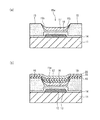
Hereinafter, embodiments of the present invention will be described in detail with reference to the drawings. FIG. 1 is a schematic cross-sectional view illustrating a configuration of an organic light emitting
図1に示すように、有機発光表示装置10は、基板11の片側主面上に、第1電極としての陽極12、ITO層13、ホール注入層14、隔壁層15、有機機能層としてのホール輸送層16、有機発光層17、電子注入層18、第2電極としての陰極19、封止層20を同順に積層して構成される。有機発光層17等は、隔壁層15の開口15aに形成されている。また、上述のように、陽極12および陰極19には直流電源が接続されている。
As shown in FIG. 1, the organic light emitting
図2に示すように、有機発光層17の平面形状は、例えば、長辺を有する角丸の長方形状である。しかしながら、これに限らず、有機発光層17の平面形状は、長軸のいずれか一方またはこれら双方を有する形状、円形状、六角形状等であってもよい。なお、有機発光層17の設けられている箇所が、隔壁層15の開口15aに該当する。以下、有機発光表示装置10における各層について詳しく説明する。
(基板11、陽極12、ITO層13)
図1に戻って、基板11は有機発光表示装置10の基材となる部分であり、例えば、無アルカリガラスからなる。しかしながら、これに限らず、基板11は、ソーダガラス、無蛍光ガラス、燐酸系ガラス、硼酸系ガラス、石英、アクリル系樹脂、スチレン系樹脂、ポリカーボネート系樹脂、エポキシ系樹脂、ポリエチレン、ポリエステル、シリコン系樹脂、またはアルミナ等の絶縁性材料で形成することができる。As shown in FIG. 2, the planar shape of the organic
(
Returning to FIG. 1, the
図示していないが、基板11の表面には有機発光表示装置10を駆動するためのTFT(薄膜トランジスタ)が形成されており、その上方に陽極12が形成されている。陽極12は、例えば、APC(銀、パラジウム、銅の合金)からなる。しかしながら、これに限らず、陽極12は、ACL(アルミニウム、コバルト、ランタンの合金)、ARA(銀、ルビジウム、金の合金)、MoCr(モリブデンとクロムの合金)、NiCr(ニッケルとクロムの合金)等で形成することができる。
Although not shown, a TFT (thin film transistor) for driving the organic light emitting
ITO(酸化インジウムスズ)層13は、陽極12とホール注入層14との間に介在し、各層間の接合性を良好にする機能を有する。なお、ITO層13は、陽極12の材料によっては、省略することもできる。
(ホール注入層14)
ホール注入層14は、ITO層13が設けられた基板11上を覆うように形成されている。また、ホール注入層14は、陽極12およびITO層13の全部を覆うように形成されると共に、隔壁層15およびホール輸送層16により覆われている。ホール注入層14は、ホールの安定化を補助したり、ホールの生成を補助したりして、有機発光層17に対しホールを注入する機能を有する。ホール注入層14は、例えば、酸化タングステンからなる。しかしながら、これに限らず、ホール注入層14は、銀(Ag)、モリブデン(Mo)、クロム(Cr)、バナジウム(V)、ニッケル(Ni)、イリジウム(Ir)等の酸化物、あるいは、PEDOT(ポリチオフェンとポリスチレンスルホン酸との混合物)等の導電性ポリマー材料で形成することができる。ただし、PEDOTなどの塗布系の材料を用いる場合は、ホール注入層14は、ITO層13が設けられた基板11上を覆うように形成されず、隔壁層15の開口15a内に形成される。
(隔壁層15)
隔壁層15には、陽極12上方に開口15aが設けられている。また、開口15aは、隔壁層15の側面である斜面15bにより囲まれている。開口15aには、ホール輸送層16および有機発光層17が設けられている。図1での断面では、隔壁層15は2つのテーパー状の隔壁として見えているが、上面視すると、図2のような層となっている。隔壁層15は、感光性レジスト材料、例えば、アクリル系樹脂からなる。しかしながら、これに限らず、隔壁層15は、ポリイミド系樹脂、ノボラック型フェノール樹脂などの絶縁性を有する有機材料で形成することができる。
(ホール輸送層16)
ホール輸送層16は凹形状に形成され、開口15aに設けられている。また、ホール輸送層16の周縁部16aは、開口15aを臨む隔壁層15の斜面15bに乗り上げている。なお、ここでいう「ホール輸送層16の周縁部16a」とは、ホール輸送層16の平坦となっている部分の端部から立ち上がっている部分の最上面までの部分をいう。ホール輸送層16は、例えば、PVK(ポリビニルカルバゾール)からなる。しかしながら、これに限らず、ホール輸送層16は、有機材料を含めばよく、例えば、ポリフルオレン系、ポリフェニレンビニレン系、ペンダント型、デンドリマー型、塗布型の低分子系を含め、溶媒に溶解させ、塗布して薄膜を形成出来る材料から形成することができる。なお、ホール輸送層16のキャリア移動度は、1.0×10⁻³(cm2/Vs)以下であればよい。
(有機発光層17)
有機発光層17は、ホール輸送層16上に設けられている。また、有機発光層17の周縁部17aの全部と隔壁層15の斜面15bとの間の全部において、ホール輸送層16が存在し、有機発光層17の周縁部17aとホール輸送層16とは接触している。また、有機発光層17の周縁部17aはホール輸送層16の周縁部16aよりも開口15aにおける内側に配されている。なお、ここでいう「有機発光層17の周縁部17a」とは、有機発光層17におけるホール輸送層16の周縁部16a上に形成された部分をいう。これにより、発明の効果が期待できるが、詳しくは後述する。有機発光層17は、有機高分子であるF8BT(poly(9、9−di−n−octylfluorene−alt−benzothiadiazole))からなる。しかしながら、これに限らず、有機発光層17は、有機発光材料を含めばよく、例えば、オキシノイド化合物、ペリレン化合物、クマリン化合物、アザクマリン化合物、オキサゾール化合物、オキサジアゾール化合物、ペリノン化合物、ピロロピロール化合物、ナフタレン化合物、アントラセン化合物、フルオレン化合物、フルオランテン化合物、テトラセン化合物、ピレン化合物、コロネン化合物、キノロン化合物およびアザキノロン化合物、ピラゾリン誘導体およびピラゾロン誘導体、ローダミン化合物、クリセン化合物、フェナントレン化合物、シクロペンタジエン化合物、スチルベン化合物、ジフェニルキノン化合物、スチリル化合物、ブタジエン化合物、ジシアノメチレンピラン化合物、ジシアノメチレンチオピラン化合物、フルオレセイン化合物、ピリリウム化合物、チアピリリウム化合物、セレナピリリウム化合物、テルロピリリウム化合物、芳香族アルダジエン化合物、オリゴフェニレン化合物、チオキサンテン化合物、シアニン化合物、アクリジン化合物、8−ヒドロキシキノリン化合物の金属錯体、2−ビピリジン化合物の金属錯体、シッフ塩とIII族金属との錯体、オキシン金属錯体、希土類錯体等の蛍光物質等を用いることができる。なお、有機発光層17の物性については後述する。
(電子注入層18、陰極19、封止層20)
電子注入層18は、隔壁15の上面および発光層17を覆うように形成されている。電子注入層18は、例えば、NaF(フッ化ナトリウム)からなる。しかしながら、これに限らず、電子注入層18は、CaF2、MgF2等で形成することができる。なお、電子注入層18は、陰極19から有機発光層17への電子の注入が十分に行われる場合は、省略してもよい。The ITO (indium tin oxide)
(Hole injection layer 14)
The
(Partition layer 15)
The
(Hole transport layer 16)
The
(Organic light emitting layer 17)
The organic
(
The
陰極19は、有機発光層17上方に電子注入層18を介して形成されている。陰極19は、例えば、ITOからなる。しかしながら、これに限らず、IZO(酸化インジウム亜鉛)等で形成することができる。また、陰極19をAl(アルミニウム)等で形成する場合には、陰極10の厚みを極小さくし、陰極19が光透過性を有するよう構成する必要がある。
The
封止層20は、陰極19上に形成されている。封止層20は、例えば、SiN(窒化シリコン)等のガスバリア性を有する材料からなる。
2.有機発光表示装置の製造方法
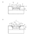
図3〜図5は、本実施の形態にかかる有機発光表示装置10の製造方法を説明する工程図である。The
2. Manufacturing Method of Organic Light-Emitting Display Device FIGS. 3 to 5 are process diagrams illustrating a manufacturing method of the organic light-emitting
まず、図3(a)に示すように、陽極12が設けられた基板11を形成する。具体的には、基板11をスパッタ成膜装置の成膜容器内に載置する。次に、成膜容器内に所定のスパッタガスを導入し、反応性スパッタリング法により陽極12を成膜する。
First, as shown in FIG. 3A, a
図3(b)に示すように、陽極12上にITO層13を形成し、ITO層13を覆うようにホール注入層14を形成する。具体的には、まず、成膜容器内で、スパッタリング法により陽極12上にITO層13を形成する。次に、スパッタリング法によりITO層13の表面および基板11の表面に金属膜を製膜する。その後、成膜された金属膜を酸化することにより、ホール注入層14が形成される。
As shown in FIG. 3B, an
次に、図3(c)に示すように開口15aが設けられた隔壁層15を形成する。ここで、上述のように、隔壁層15の材料として、例えば感光性レジスト材料を用いる。このとき、具体的には、まず、隔壁層15の材料をホール注入層14上に塗布し、プリベークした後、開口15aを形成できるようなパターンを有するマスクを重ねる。続いて、マスクの上から感光させた後、未硬化の余分な隔壁層15の材料を現像液で洗い出す。その後、純水で洗浄することで隔壁層15が形成される。
Next, as shown in FIG. 3C, a
さらに、図4(a)に示すように、開口15aにホール輸送層16の材料を含むインク16Iを塗布する。具体的には、インクジェット法により、開口15aにインク16Iを塗布する。このとき用いるインク16Iは、溶媒にPVKを、例えば、0.4wt/vol%で溶解させてなる低濃度インクである。なお、ここでいう「低濃度インク」とは、3wt/vol%以下の濃度であればよい。低濃度のインク16Iを用いることにより、塗布されるインク16Iの量は、通常の濃度のインクを用いた場合よりも増大する。そのため、塗布されたインク16Iは、開口15a上に盛りあがった形状となる。この製造方法について、詳しくは後述する。
Further, as shown in FIG. 4A, the ink 16I containing the material of the
その後、インク16Iを乾燥させることで、図4(b)に示すように、凹形状のホール輸送層16を形成する。具体的には、インク16Iを塗布した直後に、乾燥炉にてインク16Iを素早く乾燥させることで、ピニング位置が隔壁層15の最上面と同じ高さにある凹形状のホール輸送層16を得る。
Thereafter, the ink 16I is dried to form a concave
さらに、図4(c)、図5(a)に示すように、開口15aに有機発光層17の材料を含むインク17Iを塗布し、その後、インク17Iを乾燥させることで、有機発光層17を形成する。具体的には、インクジェット法によりインク17Iを塗布し、乾燥させる。また、このとき用いるインク17Iの濃度は、所望の厚みの有機発光層17を形成できる範囲内で、自由に選択することができる。このときの乾燥は、インク17Iの塗布直後に素早く乾燥させてもよいし、しばらく自然乾燥させた後、乾燥炉で乾燥させてもよい。
Furthermore, as shown in FIG. 4C and FIG. 5A, the ink 17I containing the material of the organic
最後に、図5(b)に示すように、有機発光層17上に、NaFを含む電子注入層18、Alを含む陰極19、封止層20を順に形成する。NaやAlのような低融点金属を用いるため、電子注入層18および陰極19の形成にはスパッタリング法または真空蒸着法が用いられる。封止層20の形成には、スパッタリング法、真空蒸着法、塗布法等が用いられる。
Finally, as shown in FIG. 5B, an
以上の工程を経ることで、有機発光表示装置10が完成する。
3.効果
以下、課題に対する効果を奏するための構成、および効果について説明する。本実施の形態の有機発光素子では、(3−1)開口に凹形状のホール輸送層を形成することにより有機発光層の未濡れを抑制でき、(3−2)ホール輸送層が条件1の物性を満たすことにより、リーク電流を抑制できる。また、(3−3)ホール輸送層および有機発光層が条件2〜4の物性を満たすことにより、リーク電流をさらに抑制できる。
3−1.有機発光層の未濡れの抑制
以下、(3−1)開口に凹形状のホール輸送層を形成することにより有機発光層の未濡れを抑制できる、という内容について説明する。
(概要)
発明者らは、インクジェット法を用いてホール輸送層のような有機機能層上に有機発光層を積層する場合、上方に設けられる有機発光層の形状は、下地の形状に影響を受けやすいことを見出した。また、下地が隔壁層に設けられた開口内に十分に塗り広がっている場合、下地の上に設けられる有機発光層の未濡れが起きにくいことを見出した。これらを踏まえて、開口に凹形状の有機機能層を形成し、当該有機機能層の上に有機発光層を形成することにより、有機発光層の未濡れを抑制した。
(有機機能層および有機発光層の形状)
まず、インクジェット法を用いて製造した有機発光素子における、有機機能層および有機発光層の形状について考察する。一般に、このような有機発光素子では、有機発光層の未濡れが発生するおそれがあるが、有機機能層の未濡れが発生することはない。この違いは、有機発光層および有機機能層を製造する際に用いられるインクの違いにより生じる。Through the above steps, the organic light emitting
3. Effects Hereinafter, a configuration for achieving an effect on a problem and an effect will be described. In the organic light emitting device of the present embodiment, (3-1) it is possible to suppress unwetting of the organic light emitting layer by forming a concave hole transport layer in the opening, and (3-2) the hole transport layer is in
3-1. Hereinafter, the content that (3-1) the wetness of the organic light emitting layer can be suppressed by forming a concave hole transport layer in the opening will be described.
(Overview)
The inventors have found that when an organic light emitting layer is laminated on an organic functional layer such as a hole transport layer using an inkjet method, the shape of the organic light emitting layer provided above is easily affected by the shape of the base. I found it. Further, it has been found that when the undercoat is sufficiently spread in the opening provided in the partition wall layer, the organic light emitting layer provided on the undercoat is not easily wetted. Based on these facts, a concave organic functional layer was formed in the opening, and an organic light emitting layer was formed on the organic functional layer, thereby suppressing unwetting of the organic light emitting layer.
(Shape of organic functional layer and organic light emitting layer)
First, the shapes of the organic functional layer and the organic light emitting layer in the organic light emitting device manufactured using the inkjet method will be considered. In general, in such an organic light emitting device, there is a possibility that the organic light emitting layer is not wet, but the organic functional layer is not wet. This difference is caused by a difference in ink used in manufacturing the organic light emitting layer and the organic functional layer.
ここで、有機発光層および有機機能層の材料インクについて考察する。例えば、トップエミッション型の有機発光素子では、有機発光層の下方に形成される層の厚みを、有機発光層の厚みよりも小さくすることが多い。具体的には、有機機能層の厚みが10nmであり、有機発光層の厚みが80nmであるような有機発光素子が考えられる。インクジェット法を用いる場合、各層の厚みの制御は、インクの濃度の制御により実現できる。具体的には、厚みが80nmの有機発光層を形成するために用いるインクの濃度は、厚みが10nmの有機機能層を形成するために用いるインクの濃度よりも高くすることが必要である。 Here, the material ink of the organic light emitting layer and the organic functional layer will be considered. For example, in a top emission type organic light emitting device, the thickness of the layer formed below the organic light emitting layer is often made smaller than the thickness of the organic light emitting layer. Specifically, an organic light emitting device in which the thickness of the organic functional layer is 10 nm and the thickness of the organic light emitting layer is 80 nm can be considered. When the ink jet method is used, the thickness of each layer can be controlled by controlling the ink density. Specifically, the concentration of the ink used for forming the organic light emitting layer having a thickness of 80 nm needs to be higher than the concentration of the ink used for forming the organic functional layer having a thickness of 10 nm.
ここで、各層の未濡れは、製造時に用いるインクの粘度および表面張力が大きいほど発生しやすい。そして、低濃度インクは高濃度インクと比べて粘度および表面張力が小さい。そのため、低濃度インクからなる層では、高濃度インクからなる層よりも、開口に塗り広がりやすい、という傾向がある。
そのため、低濃度インクからなる有機機能層では、未濡れの発生を抑制できる。Here, the non-wetting of each layer is more likely to occur as the viscosity and surface tension of the ink used at the time of manufacture increase. The low density ink has a lower viscosity and surface tension than the high density ink. For this reason, a layer made of low-density ink tends to spread more easily in the opening than a layer made of high-density ink.
Therefore, it is possible to suppress the occurrence of non-wetting in the organic functional layer made of low-density ink.
そして、上述のように、下地が隔壁層に設けられた開口内に十分に塗り広がっている場合、下地の上に設けられる有機発光層の未濡れが起きにくいため、有機発光層の未濡れを抑制できる。
(有機機能層の形成方法)
以下、凹形状のホール輸送層を形成する方法について説明する。凹形状のホール輸送層を形成するためには、「2.有機発光表示装置の製造方法」で述べたように、ホール輸送層の材料インクを低濃度とし、且つ、塗布したインクを、塗布直後に即座に素早く乾燥させればよい。As described above, when the base is sufficiently spread in the opening provided in the partition wall layer, the organic light emitting layer provided on the base is not easily wetted. Can be suppressed.
(Formation method of organic functional layer)
Hereinafter, a method for forming a concave hole transport layer will be described. In order to form the concave hole transport layer, as described in “2. Manufacturing method of organic light emitting display device”, the material ink of the hole transport layer is made low in concentration, and the applied ink is applied immediately after application. It can be quickly dried immediately.
まず、低濃度インクを用いる理由を述べる。通常と比べて低濃度インクを用いる場合、所望の厚みの有機機能層を形成するためには、通常と比べて多くの量の低濃度インクを塗布する必要がある。このため、低濃度インクは、高濃度インクを用いた場合よりも、隔壁層に設けられた開口に盛り上がる程度まで多く塗布される。 First, the reason for using low density ink will be described. In the case of using a low density ink as compared with the normal case, in order to form an organic functional layer having a desired thickness, it is necessary to apply a large amount of the low density ink as compared with the normal case. For this reason, more low-density ink is applied to the extent that it rises in the opening provided in the partition layer than when high-density ink is used.
次に、塗布したインクを素早く乾燥させる理由を述べる。塗布したインクを素早く乾燥させた場合には、塗布前のインクとほぼ同じ濃度の状態から即座に溶媒が蒸発し始め、完全に蒸発した後、ホール輸送層が形成される。そのため、形成されるホール輸送層のピニング点が高い位置となる。一方、インクをゆっくりと乾燥させた場合、乾燥時間の経過中にインクの濃度が徐々に高くなった後、インクから溶媒が完全に蒸発し、ホール輸送層が形成される。そのため、ホール輸送層のピニング点が低い位置となる。なお、塗布したインクを素早く乾燥させるには、例えば、インク塗布後に即座に乾燥炉にて乾燥させればよい。 Next, the reason why the applied ink is dried quickly will be described. When the applied ink is quickly dried, the solvent immediately starts to evaporate from a state of almost the same concentration as the ink before application, and after complete evaporation, a hole transport layer is formed. Therefore, the pinning point of the hole transport layer to be formed is a high position. On the other hand, when the ink is dried slowly, the concentration of the ink gradually increases during the drying time, and then the solvent is completely evaporated from the ink to form a hole transport layer. Therefore, the pinning point of the hole transport layer is a low position. In order to quickly dry the applied ink, for example, it may be dried in a drying furnace immediately after ink application.
このように、ホール輸送層の材料インクを低濃度とし、且つ、塗布したインクを素早く乾燥させることで、凹形状のホール輸送層を形成できる。
(構成および効果)
以下、有機発光素子における有機発光層の未濡れ抑制の具体例を説明する。なお、具体例では、有機機能層をホール輸送層としている。Thus, a concave hole transport layer can be formed by reducing the material ink of the hole transport layer to a low concentration and drying the applied ink quickly.
(Composition and effect)
Hereinafter, specific examples of suppression of unwetting of the organic light emitting layer in the organic light emitting device will be described. In the specific example, the organic functional layer is a hole transport layer.
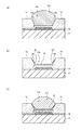
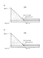
図6は、ホール輸送層の膜形状が異なる有機発光素子のイメージ図であり、図6(a)は、比較例に係る有機発光素子を示す断面図に相当し、図6(b)は、本実施の形態に係る有機発光素子を示す断面図に相当する。どちらに関しても、ホール輸送層の材料インクの濃度は、有機発光層の材料インクの濃度よりも低い。また、どちらに関しても、有機発光層の材料インクの濃度および乾燥方法は同じである。 FIG. 6 is an image diagram of an organic light emitting device having a different hole transport layer film shape. FIG. 6A corresponds to a cross-sectional view of an organic light emitting device according to a comparative example, and FIG. It is equivalent to sectional drawing which shows the organic light emitting element which concerns on embodiment. In both cases, the concentration of the material ink in the hole transport layer is lower than the concentration of the material ink in the organic light emitting layer. In both cases, the concentration of the material ink of the organic light emitting layer and the drying method are the same.
比較例では、ホール輸送層916の材料インクを塗布した後、自然乾燥を行い、最後に乾燥炉で乾燥させてホール輸送層916を得る。そのため、図6(a)に示すように、ホール輸送層916が平坦な形状である。その結果、有機発光層917の材料インクを塗布しても、インクは撥液性が高い隔壁層15の斜面15bには塗り広がりにくく、有機発光層917の未濡れは抑制できない。そして、有機発光層917の未形成領域に陰極19が形成されると、破線で囲んだ領域γにおいてホール輸送層916と陰極19とが直接接触する。これにより、陽極12から領域γにおけるホール輸送層916および陰極19へとリーク電流が流れてしまう。そして、リーク電流が流れるリークパスの距離Laは、有機機能層916の厚みに等しい。
In the comparative example, the material ink for the
一方、図6(b)に示すように、本実施の形態では、ホール輸送層16の周縁部16aが、隔壁層15の斜面15bの全部を覆うような、凹形状のホール輸送層16となっている。そのため、インクジェット法により、有機発光層17の材料インクを塗布すると、撥液性の低いホール輸送層16の周縁部16aを覆うように、インクが塗り広がりやすい。これは、上述のように、インクジェット法を用いて、ホール輸送層のような有機機能層上に有機発光層を積層する場合に、下地の上に設けられる有機発光層は、下地の形状に影響を受けやすいためである。その結果、有機発光表示装置において、有機発光層17の周縁部17aと隔壁層15の斜面15bとの間には、ホール輸送層16が存在し、有機発光層17の周縁部17aとホール輸送層16とは接触している。これにより、有機発光層17の未濡れを抑制でき、良好な発光特性を有する有機発光素子を提供できる。なお、同図において、ホール輸送層16のピニング点16bは、隔壁層15の斜面15bの最上点に一致している。しかしながら、ホール輸送層16が必ずしも隔壁層15の斜面15bの全部を覆う必要はなく、ホール輸送層16のピニング点16bが、有機発光層17の最上面と同じ高さに位置していれば、有機発光層17の未濡れを抑制できる。なお、この場合においても、破線で囲んだ領域γにおいてホール輸送層16と陰極19とが直接接触する。そのため、陽極12からホール輸送層16の周縁部16aを這い上がり、陰極19へとリーク電流が流れることとなる。そして、リーク電流が流れるリークパスの距離Lbは、Laよりも大きい。そのため、比較例と比べて、本発明ではリーク電流が抑制できる。
On the other hand, as shown in FIG. 6B, in the present embodiment, the
また、有機発光表示装置10において、ホール注入層14は、陽極12とホール輸送層16との間以外の領域にも拡がっている。ホール注入層14のうち陽極12とホール輸送層16との間以外の領域に拡がった部分は、基板11と隔壁層15との間に存在する。これにより、ホール注入層14が隔壁15の斜面15bを覆うこと無いので、ホール注入層14がリークパスとなることは無い。従って、ホール注入層14のキャリア移動度を大きくすることができ、有機発光層10の発光効率を向上できる。
3−2.有機機能層の物性の選択
(概要)
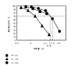
以下、(3−1)で示した構成の有機発光素子について、有機機能層と陰極との間にリークパスが発生しリーク電流により発光効率が低下する、という問題の解決について説明する。発明者らは、有機機能層と陰極との間のリークパスによる発光効率の低下を抑制するには、有機機能層のキャリア移動度を、1.0×10⁻³(cm2/Vs)以下に抑えればよいことを見出した。これは、有機機能層のキャリア移動度を変化させたときの発光効率の変化を、シミュレーションにより求めることで明らかになった。以下、シミュレーションの形態および4つの条件について詳しく述べる。
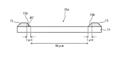
(シミュレーションの形態)
図7は、シミュレーションに用いた有機発光素子の断面図である。基板11上に、開口15aが設けられた隔壁層15が設けられている。開口15aの底部の幅は98μmである。隔壁層15の斜面15bの基板11に対する傾斜角は45°であり、隔壁層15の斜面15bに対応する底部の幅は1μmである。この有機発光素子について、理想的であると考えられる有機機能層が平坦な形状を有するものと、有機機能層が凹形状を有するものとの2つにおいて、それぞれ有機機能層の厚みが10nmかつ有機発光層の厚みが50nmの場合と、有機機能層の厚みが10nmかつ有機発光層の厚みが80nmの場合との2つの組み合わせを想定してシミュレーションを行った。以下、より具体的に説明する。In the organic light emitting
3-2. Selection of physical properties of organic functional layer (outline)
Hereinafter, regarding the organic light emitting device having the configuration shown in (3-1), a solution to the problem that a leakage path is generated between the organic functional layer and the cathode and the light emission efficiency is reduced due to the leakage current will be described. In order to suppress a decrease in light emission efficiency due to a leak path between the organic functional layer and the cathode, the inventors set the carrier mobility of the organic functional layer to 1.0 × 10 −3 (cm 2 / Vs) or less. I found out that it should be suppressed. This was clarified by determining the change in luminous efficiency by changing the carrier mobility of the organic functional layer by simulation. Hereinafter, the simulation mode and the four conditions will be described in detail.
(Simulation form)
FIG. 7 is a cross-sectional view of the organic light emitting device used in the simulation. On the
図8は、シミュレーションに用いた平坦な形状を有する有機機能層を備えた有機発光素子910a、910bにおける隔壁層近傍の拡大図である。図8(a)は有機機能層の厚みが10nmかつ有機発光層の厚みが80nmの場合であり、図8(b)は有機機能層の厚みが10nmかつ有機発光層の厚みが50nmの場合に対応する。図9は、シミュレーションに用いた凹形状を有する有機機能層を備えた有機発光素子10a、10bにおける隔壁層近傍の拡大図である。図9(a)は有機機能層の厚みが10nmかつ有機発光層の厚みが80nmの場合であり、図9(b)は有機機能層の厚みが10nmかつ有機発光層の厚みが50nmの場合に対応する。なお、図8、図9における点の座標は、その点を(X,Y)で示した時の座標である。
FIG. 8 is an enlarged view of the vicinity of the partition layer in the organic
図8(a)、図8(b)に示すように、平坦な形状の有機機能層16の周縁部の最上点16Aは(0.99,0.01)である。また、有機発光層17の周縁部の最上点17Aは、図8(a)では(0.91,0.09)であり、図8(b)では(0.94,0.06)である。
As shown in FIGS. 8A and 8B, the uppermost point 16A of the peripheral portion of the organic
一方、図9(a)、図9(b)に示すように、凹形状の有機機能層16のピニング点16Pは、(0,1)であり、有機機能層16が平坦となる箇所の端点16Bは、(1,0.01)である。また、有機発光層17のピニング点17Bは、(0.2,0.8)であり、有機発光層17が平坦となる箇所の端点17Bは、図9(a)では(0.95、0.09)であり、図9(b)では(0.98,0.06)である。
On the other hand, as shown in FIGS. 9A and 9B, the pinning
なお、シミュレーションでは、図8に示した平坦な形状の有機機能層を備えた有機発光素子910a、910bの発光効率を基準とし、図9に示した凹形状の有機機能層を備えた有機発光素子10a、10bの発光効率の比を相対発光効率として見積もった。さらに、平面な形状の有機機能層を備えた有機発光素子910a、910bに対して、凹形状の有機機能層を備えた有機発光素子10a、10bの発光効率の低下が抑制されるか否かを評価した。なお、ここでの発光効率の低下の抑制とは、相対発光効率が70%以上である場合を指す。
(条件1:有機発光層のキャリア移動度)
発明者らは、発光効率に対する有機機能層のキャリア移動度の影響を検証するシミュレーションを行った。シミュレーションに用いた有機発光素子の物性は、表1(a)の通りである。In the simulation, the organic light emitting device having the concave organic functional layer shown in FIG. 9 is based on the light emission efficiency of the organic
(Condition 1: Carrier mobility of organic light emitting layer)
The inventors conducted a simulation to verify the influence of the carrier mobility of the organic functional layer on the luminous efficiency. The physical properties of the organic light-emitting device used for the simulation are as shown in Table 1 (a).
これらの条件の下、シミュレーションした結果を表2(a)に示し、表2(a)をもとに作製したグラフを図10に示す。 The simulation results under these conditions are shown in Table 2 (a), and a graph produced based on Table 2 (a) is shown in FIG.
図10は、発光効率に対する有機機能層のキャリア移動度の影響を示す図である。図10において、横軸が有機機能層のキャリア移動度(cm2/Vs)、縦軸が相対発光効率(%)をそれぞれ示す。FIG. 10 is a diagram showing the influence of the carrier mobility of the organic functional layer on the luminous efficiency. In FIG. 10, the horizontal axis represents the carrier mobility (cm 2 / Vs) of the organic functional layer, and the vertical axis represents the relative luminous efficiency (%).
平坦な形状の有機発光素子910a、910bの発光効率を基準とした場合、図10に示すように、有機機能層のキャリア移動度の増加に伴い、相対発光効率が低下する。より詳しく見ると、ケース1〜3の全てにおける有機機能層のキャリア移動度が1.0×10⁻³(cm2/Vs)以上の範囲では相対発光効率の低下が著しく、1.0×10-4(cm2/Vs)以上1.0×10-3(cm2/Vs)以下の範囲では相対発光効率の低下が抑制されている。そのため、有機機能層のキャリア移動度の閾値を、1.0×10-3(cm2/Vs)とした。なお、有機機能層のキャリア移動度が1.0×10-4(cm2/Vs)以下の範囲では、さらに発光効率への影響は減少すると考えられる。これは、有機機能層のキャリア移動度が1.0×10-4(cm2/Vs)以下であれば、平坦な形状の有機機能層を備えた有機発光素子910a、910bにおいても発光効率が低下してしまい、凹形状の有機機能層を備えた有機発光素子10a、10bとの差が小さくなると考えられるためである。When the light emission efficiency of the flat organic
従って、有機機能層のキャリア移動度が1.0×10⁻³(cm2/Vs)以下であれば、良好な発光特性を得ることができる。
3−3.有機機能層および有機発光層の物性の選択
(概要)
以下、さらに確実に良好な発光特性を得ることができる有機機能層および有機発光層の物性について説明する。具体的には、(3−2)と同様のシミュレーションにより、条件2〜4を求めたので、これについて述べる。
(条件2:有機発光層のキャリア移動度)
発明者らは、発光効率に対する有機発光層のキャリア移動度の影響を検証するシミュレーションを行った。また有機機能層と有機発光層とのHOMO(Highest Occupied Molecular Orbital)のエネルギー差(以下、「有機機能層と有機発光層とのHOMO差」と呼ぶ)については、表1(b)に示す値の、3つ組み合わせでシミュレーションした。シミュレーションに用いた有機発光素子の物性は、表1(b)の通りである。なお、有機機能層と有機発光層とのHOMO差は、各層のエネルギー障壁に相当する。Therefore, when the carrier mobility of the organic functional layer is 1.0 × 10 −3 (cm 2 / Vs) or less, good light emission characteristics can be obtained.
3-3. Selection of physical properties of organic functional layer and organic light emitting layer (outline)
Hereinafter, the physical properties of the organic functional layer and the organic light-emitting layer capable of more reliably obtaining good light-emitting characteristics will be described. Specifically, conditions 2 to 4 were obtained by a simulation similar to (3-2), which will be described.
(Condition 2: Carrier mobility of organic light emitting layer)
The inventors conducted a simulation to verify the influence of the carrier mobility of the organic light emitting layer on the luminous efficiency. The energy difference of HOMO (High Occupied Molecular Orbital) between the organic functional layer and the organic light emitting layer (hereinafter referred to as “HOMO difference between the organic functional layer and the organic light emitting layer”) is a value shown in Table 1 (b). The three combinations were simulated. Table 1 (b) shows the physical properties of the organic light-emitting element used in the simulation. Note that the HOMO difference between the organic functional layer and the organic light emitting layer corresponds to the energy barrier of each layer.
表1(b)に示す有機機能層のキャリア移動度は、(条件1)で発光効率の低下抑制のための閾値と規定した1.0×10⁻³(cm2/Vs)の値である。The carrier mobility of the organic functional layer shown in Table 1 (b) is a value of 1.0 × 10 −3 (cm 2 / Vs) defined as a threshold value for suppressing a decrease in luminous efficiency in (Condition 1). .
これらの条件の下、シミュレーションした結果を表2(b)に示し、表2(b)をもとに作製したグラフを図11に示す。 The simulation results under these conditions are shown in Table 2 (b), and a graph produced based on Table 2 (b) is shown in FIG.
図11は、発光効率に対する有機発光層のキャリア移動度の影響を示す図である。図11において、横軸が有機発光層のキャリア移動度(cm2/Vs)、縦軸が相対発光効率(%)をそれぞれ示す。FIG. 11 is a diagram illustrating the influence of the carrier mobility of the organic light emitting layer on the light emission efficiency. In FIG. 11, the horizontal axis represents the carrier mobility (cm 2 / Vs) of the organic light emitting layer, and the vertical axis represents the relative luminous efficiency (%).
図11において、ケース1、ケース2では、有機発光層のキャリア移動度が6.3×10⁻⁸(cm2/Vs)以上であれば、凹形状の有機機能層を備えた有機発光素子10a、10bの発光効率の低下が30%以内に抑制される。一方、ケース3では、凹形状の有機機能層を備えた有機発光素子10a、10bの発光効率の低下抑制のために、有機発光層のキャリア移動度が6.3×10-8(cm2/Vs)以上ということは、発光効率の低下の抑制には必要条件では有るが十分条件ではないといえる。
(条件3:有機機能層と有機発光層とのエネルギー障壁)
さらに、発明者らは、発光効率に対する有機機能層と有機発光層とのエネルギー障壁の影響を検証するシミュレーションを行った。シミュレーションに用いた有機発光素子の物性(有機機能層のキャリア移動度と有機発光層のキャリア移動度)は、表1(c)の通りである。In FIG. 11, in
(Condition 3: Energy barrier between the organic functional layer and the organic light emitting layer)
Furthermore, the inventors performed a simulation to verify the influence of the energy barrier between the organic functional layer and the organic light emitting layer on the light emission efficiency. The physical properties (carrier mobility of the organic functional layer and carrier mobility of the organic light emitting layer) of the organic light emitting element used for the simulation are as shown in Table 1 (c).
有機機能層のキャリア移動度については、(条件1)で発光効率の低下抑制のための閾値と規定した1.0×10⁻³(cm2/Vs)の値を用いた。For the carrier mobility of the organic functional layer, the value of 1.0 × 10 −3 (cm 2 / Vs) defined as the threshold value for suppressing the decrease in luminous efficiency in (Condition 1) was used.
これらの条件の下、シミュレーションした結果を表2(c)に示し、表2(c)をもとに作製したグラフを図12に示す。 The simulation results under these conditions are shown in Table 2 (c), and a graph produced based on Table 2 (c) is shown in FIG.
図12は、発光効率に対する有機機能層と有機発光層とのHOMO差の影響を示す図である。図12において、横軸が有機発光層と有機機能層とのHOMO差(eV)、縦軸が相対発光効率(%)をそれぞれ示す。 FIG. 12 is a diagram showing the influence of the HOMO difference between the organic functional layer and the organic light emitting layer on the light emission efficiency. In FIG. 12, the horizontal axis represents the HOMO difference (eV) between the organic light emitting layer and the organic functional layer, and the vertical axis represents the relative light emission efficiency (%).
図12において、ケース1、3では、有機機能層と有機発光層とのHOMO差が0.28(eV)以下であれば、凹形状の有機機能層を備えた有機発光素子10a、10bの発光効率の低下が抑制されることが示された。一方、ケース2において、発光効率の低下抑制のために、HOMO差が0.28(eV)以下であることは、必要条件では有るが十分条件ではないといえる。
(条件4:有機機能層と有機発光層とのHOMO差と、有機発光層のキャリア移動度との相関)
上述のように、(条件2)有機発光層のキャリア移動度が6.3×10⁻⁸(cm2/Vs)以上であること、および(条件3)有機発光層と有機機能層とのHOMO差が0.28(eV)以下であることは、ケース1〜3すべてにおいて必要条件であるが、必ずしも十分条件であるわけではない。そこで、発明者らは、発光効率に対する有機機能層と有機発光層とのHOMO差、および有機発光層のキャリア移動度の相関についてシミュレーションを行い検証した。シミュレーションに用いた有機発光素子の物性は、表1(d)の通りである。12, in
(Condition 4: Correlation between HOMO difference between organic functional layer and organic light emitting layer and carrier mobility of organic light emitting layer)
As described above, (Condition 2) The carrier mobility of the organic light emitting layer is 6.3 × 10 −8 (cm 2 / Vs) or more, and (Condition 3) HOMO between the organic light emitting layer and the organic functional layer. A difference of 0.28 (eV) or less is a necessary condition in all
ケース1〜3では、それぞれ有機発光層の材料が異なる。これらの条件の下、シミュレーションした結果を図13に示す。
In
同図は、発光効率に対する有機機能層と有機発光層とのHOMO差および有機発光層のキャリア移動度の相関を示す図である。同図において、横軸が有機発光層のキャリア移動度(eV)、縦軸が有機発光層と有機機能層とのHOMO差(eV)をそれぞれ示す。また、同図において、平坦な形状の有機機能層を備えた有機発光素子910a、910bの発光効率を基準とし、基準に対する凹形状の有機機能層を備えた有機発光素子10a、10bの発光効率の比を等高線で示している。そして、相対発光効率が70%となる条件に折れ線を引き、ケース1、ケース2、ケース3の折れ線をひとつのグラフに重ねた。これにより、ケース1〜3において、相対発光効率が70%となる有機発光層のキャリア移動度および縦軸が有機発光層と有機機能層とのHOMO差が分かった。
The figure shows the correlation between the HOMO difference between the organic functional layer and the organic light emitting layer and the carrier mobility of the organic light emitting layer with respect to the luminous efficiency. In the figure, the horizontal axis represents the carrier mobility (eV) of the organic light emitting layer, and the vertical axis represents the HOMO difference (eV) between the organic light emitting layer and the organic functional layer. In addition, in the same figure, the light emission efficiency of the organic
次に、同図を用いて、ケース1〜3において、相対発光効率が70%以上になる相対発光効率が良好な範囲について検討した。
Next, the range in which the relative luminous efficiency is good in
有機発光層のキャリア移動度が小さいとき、有機機能層と有機発光層との界面でホールの少ない領域が発生しにくくなる。そのため、有機機能層から有機発光層にホールが移動しにくくなる。その結果、有機機能層から有機発光層へのキャリア注入性が低下する。また、有機発光層と有機機能層とのHOMO差が大きいときも、有機機能層から有機発光層へのキャリア注入性が低下する。そのため、有機発光層のキャリア移動度が小さく、且つ、有機発光層と有機機能層とのHOMO差が大きいとき、有機機能層から有機発光層への電流に対して、有機機能層の周縁部を介したリーク電流が流れやすくなり相対発光効率が小さくなる。この領域が同図における左上の領域である。一方、有機発光層のキャリア移動度が大きく、且つ、有機発光層と有機機能層とのHOMO差が小さいとき、有機機能層から有機発光層へのキャリア注入性が向上する。そのため、有機機能層の周縁部を介したリーク電流が流れにくくなり相対発光効率が大きくなる。このように、同図における右下の領域ほど、相対発光効率は向上する。 When the carrier mobility of the organic light emitting layer is small, a region with few holes is hardly generated at the interface between the organic functional layer and the organic light emitting layer. Therefore, it becomes difficult for holes to move from the organic functional layer to the organic light emitting layer. As a result, the carrier injection property from the organic functional layer to the organic light emitting layer is lowered. Also, when the HOMO difference between the organic light emitting layer and the organic functional layer is large, the carrier injection property from the organic functional layer to the organic light emitting layer is lowered. Therefore, when the carrier mobility of the organic light emitting layer is small and the HOMO difference between the organic light emitting layer and the organic functional layer is large, the peripheral portion of the organic functional layer is set against the current from the organic functional layer to the organic light emitting layer. Leakage current is likely to flow, and the relative luminous efficiency is reduced. This area is the upper left area in FIG. On the other hand, when the carrier mobility of the organic light emitting layer is large and the HOMO difference between the organic light emitting layer and the organic functional layer is small, the carrier injection property from the organic functional layer to the organic light emitting layer is improved. Therefore, it is difficult for a leak current to flow through the peripheral edge of the organic functional layer, and the relative light emission efficiency is increased. Thus, the relative light emission efficiency is improved in the lower right region in FIG.
ここで、ケース1〜3の折れ線のうち、ケース3の折れ線が、発光効率の最も小さくなるケースである。例えば、有機発光層のキャリア移動度が1.39×10⁻⁵(cm2/Vs)および有機発光層と有機機能層とのHOMO差0.23(eV)であるときケース1では相対発光効率が70%であるが、ケース3では相対発光効率は70%未満である。このように、ケース1〜3の折れ線のすべてにおいて相対発光効率が70%以上となる範囲を満たせば、いかなる材料からなる有機発光層を備えた有機発光素子であっても発光効率の低下を抑制できる。以下、この範囲について検討する。Here, among the broken lines of
有機発光層のキャリア移動度が1.0×10⁻⁹(cm2/Vs)以上1.0×10-4(cm2/Vs)以下の範囲において、ケース1〜3の折れ線すべてにおいて相対発光効率が70%以上となるのは、有機発光層のキャリア移動度および有機発光層と有機機能層とのHOMO差が数1を満たす範囲である。When the carrier mobility of the organic light emitting layer is in the range of 1.0 × 10 −9 (cm 2 / Vs) to 1.0 × 10 −4 (cm 2 / Vs), the relative light emission occurs in all the broken lines of
同図における二点鎖線よりも下方が数1に相当する。 Below the two-dot chain line in FIG.
一方、有機発光層のキャリア移動度が1.0×10⁻⁴(cm2/Vs)以上1.0×10-1(cm2/Vs)以下の範囲において、ケース1〜3の折れ線すべてにおいて相対発光効率が70%となるのは、有機発光層のキャリア移動度および有機発光層と有機機能層とのHOMO差が数2を満たす範囲である。On the other hand, in the case where the carrier mobility of the organic light emitting layer is 1.0 × 10 −4 (cm 2 / Vs) or more and 1.0 × 10 −1 (cm 2 / Vs) or less, all the broken lines of
同図における一点鎖線よりも下方が数2に相当する。 The part below the one-dot chain line in FIG.
ところで、有機発光層の材料開発により、相対発光効率が70%となるときの有機発光層のキャリア移動度および有機機能層と有機発光層とのHOMO差は多少変動すると考えられる。これに対し、発明者らが過去に材料を変更して行ったシミュレーションを考慮すると、ケース1、ケース2、ケース3に対する当該変動の大きさはそれぞれ約5%と見積もられた。そのため、どのような構成の有機発光素子であっても、相対発光効率が70%となるときの有機発光層のキャリア移動度および有機発光層と有機機能層とのHOMO差はケース1、ケース2、ケース3付近に現れる、といえる。
By the way, it is considered that the carrier mobility of the organic light-emitting layer and the HOMO difference between the organic functional layer and the organic light-emitting layer when the relative light emission efficiency is 70% are slightly changed due to the development of the material of the organic light-emitting layer. On the other hand, when considering the simulations performed by the inventors in the past by changing the material, the magnitude of the variation for
従って、ケース1〜3の全部において、凹形状の有機機能層を備えた有機発光素子10a、10bの発光効率の低下を抑制できる領域は、数1、数2を満たす範囲であることが明らかとなった
条件2〜4を満たす有機機能層および有機発光層を用いれば、さらに良好な発光特性を得ることができる。
(有機機能層および有機発光層の具体例)
条件1〜4の物性を満たす有機機能層および有機発光層を選択することで、さらに良好な発光特性を有する有機発光素子を得ることが可能となる。具体的には、有機機能層として、PVK(ポリビニルカルバゾール)を用い、有機発光層としてF8(フルオレン)系材料を用いることができる。PVKのキャリア移動度は、1.0×10⁻⁵(cm2/Vs)〜1.0×10-6(cm2/Vs)であり(参考文献:特開平11−144525)、(条件1)を満たす。F8系材料のキャリア移動度は、5×10-3(cm2/vs)であり(参考文献:特開2008−282957)、(条件2)を満たす。また、PVKのHOMOの値は5.6(eV)〜5.9(eV)程度であり(参考文献:特開2001−284060、J.Kido,H.Shionoya and K.Nagai,Appl.Phys.Lett.67 2881 (1995))、F8系材料のHOMOの値は5.8(eV)程度である(参考文献:Adv.Mater.2004.16.No.6.March.18)ことが一般的に知られている。そのため、有機機能層として、PVK(ポリビニルカルバゾール)を用い、有機発光層としてF8(フルオレン)系材料を用いれば、有機発光層と有機機能層とのHOMO差が、0.2(eV)以下となり、(条件3)および(条件4)を満たす。従って、上記材料を用いれば有機機能層と有機発光層とは、(条件1〜4)を満たすこととなる。
<変形例>
以上、実施の形態を説明したが、以下のような変形例が考えられる。
(1)有機機能層、有機発光層、および隔壁の形状
上記実施の形態では、有機発光層の周縁部の全部と隔壁層の斜面との間に、有機機能層が存在している。しかしながら、この構成に限らず、有機発光層の周縁部の少なくとも一部と隔壁層の斜面との間に、有機機能層が存在していれば、発明の効果を期待できる。なお、ここでいう「周縁部の少なくとも一部」とは、周縁部のうち誤差範囲を除く部分をいう。
(2)有機発光表示装置
上記実施の形態では、有機発光表示装置における有機発光層の発光色については言及しなかった。しかしながら、単色表示に限らず、フルカラー表示の有機発光表示装置にも適用できる。フルカラー表示の有機発光表示装置においては、1つの有機発光素子が、RGB各色のサブピクセルに相当し、隣り合うRGBのサブピクセルが組み合わさって一画素が形成され、この画素がマトリックス状に配列されて画像表示領域が形成される。Therefore, in all of
(Specific examples of organic functional layer and organic light emitting layer)
By selecting an organic functional layer and an organic light emitting layer satisfying the physical properties of
<Modification>
Although the embodiment has been described above, the following modifications can be considered.
(1) Shape of Organic Functional Layer, Organic Light-Emitting Layer, and Partition In the above embodiment, the organic functional layer exists between the entire peripheral edge of the organic light-emitting layer and the slope of the partition layer. However, the present invention is not limited to this configuration, and the effect of the invention can be expected if an organic functional layer exists between at least a part of the peripheral edge of the organic light emitting layer and the slope of the partition wall layer. Here, “at least a part of the peripheral portion” refers to a portion of the peripheral portion excluding the error range.
(2) Organic Light-Emitting Display Device In the above embodiment, the light emission color of the organic light-emitting layer in the organic light-emitting display device is not mentioned. However, the present invention is not limited to single color display and can be applied to organic light emitting display devices for full color display. In an organic light emitting display device for full color display, one organic light emitting element corresponds to a subpixel of each RGB color, and one pixel is formed by combining adjacent RGB subpixels, and the pixels are arranged in a matrix. Thus, an image display area is formed.
また、上記実施の形態では、トップエミッション型の有機発光表示装置を例に説明したが、ボトムエミッション型の有機発光表示装置における有機発光層を形成する場合にも同様に実施可能である。
(3)有機機能層および有機発光層の製造方法
上記実施の形態では、有機機能層の材料であるインクの濃度を調整し、インクの乾燥方法を規定することで、凹形状の有機機能層を形成した。しかしながら、これに限らず、例えば、開口を臨む隔壁層の斜面の撥液性を低減する、すなわち、濡れ性を高くすることで、有機機能層の材料であるインクを凸形状に盛り、有機機能層のピニング点を高い位置にしてもよい。具体的には、隔壁層を形成した後、UV(ultraviolet)線を照射することにより、開口を臨む隔壁層の斜面の濡れ性を高めることができる。In the above embodiment, the top emission type organic light emitting display device has been described as an example. However, the present invention can be similarly applied to the case of forming an organic light emitting layer in a bottom emission type organic light emitting display device.
(3) Manufacturing Method of Organic Functional Layer and Organic Light-Emitting Layer In the above embodiment, the concave organic functional layer is formed by adjusting the concentration of the ink that is the material of the organic functional layer and defining the ink drying method. Formed. However, the present invention is not limited to this, for example, by reducing the liquid repellency of the slope of the partition wall layer facing the opening, that is, by increasing the wettability, the ink that is the material of the organic functional layer is deposited in a convex shape, and the organic function The pinning point of the layer may be high. Specifically, the wettability of the slope of the partition layer facing the opening can be enhanced by irradiating UV (ultraviolet) rays after the partition layer is formed.
また、上記実施の形態では、有機機能層および発光層をインクジェット法による塗布方式で製造した。しかしながら、これに限らず、有機機能層および発光層は、例えば、スピンコート法、グラビア印刷法、ディスペンサー法、ノズルコート法、凹版印刷、凸版印刷等の公知の方法によりインクを滴下および塗布してもよい。
(4)有機機能層と有機発光層との材料
上記実施の形態では、有機機能層としてPVKを用い、有機発光層としてF8系材料を用いた。しかしながら、これに限らず、凹形状の有機機能層の形成が可能であり、且つ、有機機能層のキャリア移動度が1.0×10⁻³(cm2/Vs)以下であることを満たせば、有機機能層と有機発光層との材料は他のものを用いてもよい。
(5)有機機能層の機能
上記実施の形態では、有機機能層をホール輸送の機能を有するものとした。しかしながら、これに限らず、有機機能層は、キャリアを輸送する機能、キャリア注入の機能、あるいはキャリアの輸送をブロックする機能を有するものであってもよい。ここでいう「キャリア」とは、ホールに限らず、電子であってもよい。
(6)その他
上記実施の形態では示していないが、基板上に金属製の補助配線を設けてもよい。陰極の周縁部から電圧が印加されている場合、当該補助配線と陰極とを電気的に接続することにより、陰極の中央部と周縁部とで電圧がばらつくことを抑制できる。Moreover, in the said embodiment, the organic functional layer and the light emitting layer were manufactured with the application | coating system by the inkjet method. However, the organic functional layer and the light emitting layer are not limited to this, and the ink is dropped and applied by a known method such as a spin coating method, a gravure printing method, a dispenser method, a nozzle coating method, an intaglio printing, and a relief printing. Also good.
(4) Material of an organic functional layer and an organic light emitting layer In the said embodiment, PVK was used as an organic functional layer, and F8 type material was used as an organic light emitting layer. However, the present invention is not limited to this, as long as it is possible to form a concave organic functional layer and that the carrier mobility of the organic functional layer is 1.0 × 10 −3 (cm 2 / Vs) or less. Other materials may be used for the organic functional layer and the organic light emitting layer.
(5) Function of organic functional layer In the said embodiment, the organic functional layer shall have the function of hole transport. However, the organic functional layer is not limited to this, and the organic functional layer may have a function of transporting carriers, a function of injecting carriers, or a function of blocking transport of carriers. The “carrier” here is not limited to holes, but may be electrons.
(6) Others Although not shown in the above embodiment, metal auxiliary wiring may be provided on the substrate. When a voltage is applied from the peripheral edge of the cathode, the auxiliary wiring and the cathode are electrically connected to suppress voltage variation between the central portion and the peripheral edge of the cathode.
本発明の一態様に係る有機発光素子およびそれを用いた有機発光表示装置は、ウェットプロセス法による有機発光素子の製造プロセスに広く利用できる。また、ドライプロセス法においても適応できる。また、本発明の一態様に係る有機発光素子は、例えば、パッシブマトリクス型あるいはアクティブマトリクス型の有機表示装置および有機発光装置の分野全般等で広く利用できる。 The organic light-emitting device and the organic light-emitting display device using the organic light-emitting device according to one embodiment of the present invention can be widely used in manufacturing processes of organic light-emitting devices by a wet process method. It can also be applied to dry process methods. In addition, the organic light-emitting element according to one embodiment of the present invention can be widely used in, for example, the general field of passive matrix or active matrix organic display devices and organic light-emitting devices.
10:有機発光表示装置
11:基板
12:陽極
13:ITO層
14:ホール注入層
15:隔壁層
15a:開口
15b:斜面
16:ホール輸送層
17:有機発光層
17a:周縁部
18:電子注入層
19:陰極
20:封止層10: Organic light emitting display device 11: Substrate 12: Anode 13: ITO layer 14: Hole injection layer 15:
Claims (8)
前記基板上に設けられた第1電極と、
前記基板上に設けられ、前記第1電極上方に開口を有する隔壁層と、
前記開口内に設けられ、有機材料を含む有機機能層と、
前記有機機能層上に設けられ、有機発光材料を含む有機発光層と、
前記有機発光層上方に設けられた第2電極と、
を有し、
前記有機発光層の周縁部の少なくとも一部と前記開口を臨む前記隔壁層の側面との間には、前記有機機能層が存在し、
前記有機機能層のキャリア移動度は、1.0×10⁻³(cm2/Vs)以下である、
有機発光素子。A substrate,
A first electrode provided on the substrate;
A partition layer provided on the substrate and having an opening above the first electrode;
An organic functional layer provided in the opening and containing an organic material;
An organic light emitting layer provided on the organic functional layer and containing an organic light emitting material;
A second electrode provided above the organic light emitting layer;
Have
The organic functional layer exists between at least a part of the peripheral edge of the organic light emitting layer and the side surface of the partition layer facing the opening,
The carrier mobility of the organic functional layer is 1.0 × 10 −3 (cm 2 / Vs) or less.
Organic light emitting device.
前記有機発光層のキャリア移動度は、6.3×10⁻⁸(cm2/Vs)以上であり、
前記有機発光層のキャリア移動度(X)と、前記有機機能層のHOMOと前記有機発光層のHOMOとの差(Y)とは、下記数1または数2を満たす、
請求項1記載の有機発光素子。
The carrier mobility of the organic light emitting layer is 6.3 × 10 −8 (cm 2 / Vs) or more,
The carrier mobility (X) of the organic light emitting layer and the difference (Y) between the HOMO of the organic functional layer and the HOMO of the organic light emitting layer satisfy the following formula 1 or formula 2:
The organic light emitting device according to claim 1.
前記有機機能層の周縁部は、前記開口を臨む前記隔壁層の側面に乗り上げており、
前記有機発光層の周縁部は、前記有機機能層の周縁部よりも前記開口における内側に配されている、
請求項1記載の有機発光素子。The side surface of the partition layer facing the opening is formed in a slope shape inclined with respect to the surface of the substrate,
The peripheral portion of the organic functional layer runs on the side surface of the partition layer facing the opening,
The peripheral part of the organic light emitting layer is arranged on the inner side in the opening than the peripheral part of the organic functional layer.
The organic light emitting device according to claim 1.
請求項1記載の有機発光素子。Having an intermediate layer between the organic light emitting layer and the second electrode;
The organic light emitting device according to claim 1.
請求項1記載の有機発光素子。Having a carrier injection layer between the first electrode and the organic functional layer;
The organic light emitting device according to claim 1.
前記キャリア注入層のうち前記第1電極と前記有機機能層との間以外の領域に拡がった部分は、前記基板と前記隔壁層との間に存在する、
請求項5記載の有機発光素子。The carrier injection layer extends to a region other than between the first electrode and the organic functional layer,
A portion of the carrier injection layer that extends to a region other than between the first electrode and the organic functional layer exists between the substrate and the partition layer.
The organic light emitting device according to claim 5.
前記第2電極と前記補助配線とが接触している、
請求項1記載の有機発光素子。On the substrate, there is a metal auxiliary wiring,
The second electrode is in contact with the auxiliary wiring;
The organic light emitting device according to claim 1.
前記基板上に、前記各第1電極上方に開口を有する隔壁層を形成する工程と、
前記開口内に、有機材料を含む溶液を塗布し乾燥させて、そのキャリア移動度が1.0×10⁻³(cm2/Vs)以下である有機機能層を形成する工程と、
前記有機機能層上に、有機発光材料を含む溶液を塗布し乾燥させて有機発光層を形成する工程と、
前記有機発光層上方に、第2電極を形成する工程と、
を含み、
前記有機発光層の周縁部の少なくとも一部と前記開口を臨む前記隔壁層の側面との間には、前記有機機能層が存在する、
有機発光素子の製造方法。Preparing a substrate provided with a plurality of first electrodes;
Forming a partition layer having an opening above each first electrode on the substrate;
Applying a solution containing an organic material in the opening and drying to form an organic functional layer having a carrier mobility of 1.0 × 10 −3 (cm 2 / Vs) or less;
Applying a solution containing an organic light emitting material on the organic functional layer and drying to form an organic light emitting layer;
Forming a second electrode above the organic light emitting layer;
Including
The organic functional layer is present between at least a part of the peripheral edge of the organic light emitting layer and the side surface of the partition layer facing the opening.
Manufacturing method of organic light emitting element.
Priority Applications (1)
| Application Number | Priority Date | Filing Date | Title |
|---|---|---|---|
| JP2014520961A JPWO2013190847A1 (en) | 2012-06-20 | 2013-06-20 | ORGANIC LIGHT EMITTING ELEMENT AND MANUFACTURING METHOD THEREOF |
Applications Claiming Priority (4)
| Application Number | Priority Date | Filing Date | Title |
|---|---|---|---|
| JP2012138378 | 2012-06-20 | ||
| JP2012138378 | 2012-06-20 | ||
| PCT/JP2013/003878 WO2013190847A1 (en) | 2012-06-20 | 2013-06-20 | Organic light-emitting element and production method therefor |
| JP2014520961A JPWO2013190847A1 (en) | 2012-06-20 | 2013-06-20 | ORGANIC LIGHT EMITTING ELEMENT AND MANUFACTURING METHOD THEREOF |
Publications (1)
| Publication Number | Publication Date |
|---|---|
| JPWO2013190847A1 true JPWO2013190847A1 (en) | 2016-02-08 |
Family
ID=49768458
Family Applications (1)
| Application Number | Title | Priority Date | Filing Date |
|---|---|---|---|
| JP2014520961A Pending JPWO2013190847A1 (en) | 2012-06-20 | 2013-06-20 | ORGANIC LIGHT EMITTING ELEMENT AND MANUFACTURING METHOD THEREOF |
Country Status (3)
| Country | Link |
|---|---|
| US (1) | US20150155516A1 (en) |
| JP (1) | JPWO2013190847A1 (en) |
| WO (1) | WO2013190847A1 (en) |
Families Citing this family (18)
| Publication number | Priority date | Publication date | Assignee | Title |
|---|---|---|---|---|
| KR102242078B1 (en) | 2014-08-05 | 2021-04-21 | 삼성디스플레이 주식회사 | Oranic light emitting display devices and methods of manufacturing the same |
| US11711958B2 (en) | 2014-09-11 | 2023-07-25 | Boe Technology Group Co., Ltd. | Display panel and display device |
| US11004905B2 (en) * | 2014-09-11 | 2021-05-11 | Boe Technology Group Co., Ltd. | Display panel and display device |
| JP2016091942A (en) * | 2014-11-10 | 2016-05-23 | 株式会社Joled | Display device and manufacture method thereof |
| CN104779268B (en) * | 2015-04-13 | 2016-07-06 | 深圳市华星光电技术有限公司 | Oled display device |
| CN104795429B (en) * | 2015-04-13 | 2017-09-01 | 深圳市华星光电技术有限公司 | Oled display device |
| KR102574052B1 (en) * | 2015-11-19 | 2023-09-04 | 엘지디스플레이 주식회사 | Organic light emitting display device |
| US10374183B2 (en) * | 2015-11-19 | 2019-08-06 | Lg Display Co., Ltd. | Organic light emitting display device having layer to control charge transfer |
| JP6640034B2 (en) * | 2016-06-17 | 2020-02-05 | 株式会社ジャパンディスプレイ | Manufacturing method of organic EL display device |
| JP2018181970A (en) * | 2017-04-07 | 2018-11-15 | 株式会社ジャパンディスプレイ | Display, and method for manufacturing display |
| GB2563448A (en) * | 2017-06-16 | 2018-12-19 | Sumitomo Chemical Co | Device |
| JP6768616B2 (en) * | 2017-09-19 | 2020-10-14 | 株式会社Joled | Display device and manufacturing method of display device |
| KR102456458B1 (en) * | 2017-12-27 | 2022-10-18 | 엘지디스플레이 주식회사 | Electroluminescent Display Device |
| US11730017B2 (en) * | 2018-11-13 | 2023-08-15 | Samsung Display Co., Ltd. | Display device and method of fabricating the same |
| JP2020097758A (en) * | 2018-12-17 | 2020-06-25 | 住友化学株式会社 | Particle for vacuum deposition |
| JP2019102466A (en) * | 2019-01-17 | 2019-06-24 | 堺ディスプレイプロダクト株式会社 | Organic el light-emitting element and method for manufacturing the same |
| JP6966607B2 (en) * | 2019-01-17 | 2021-11-17 | 堺ディスプレイプロダクト株式会社 | Organic EL light emitting device and its manufacturing method |
| KR20210083989A (en) * | 2019-12-27 | 2021-07-07 | 엘지디스플레이 주식회사 | Display panel and display device including the same |
Citations (12)
| Publication number | Priority date | Publication date | Assignee | Title |
|---|---|---|---|---|
| JP2002507825A (en) * | 1998-03-13 | 2002-03-12 | ケンブリッジ ディスプレイ テクノロジー リミテッド | Electroluminescence element |
| JP2003249376A (en) * | 2001-12-18 | 2003-09-05 | Seiko Epson Corp | Display device and electronic equipment |
| JP2004288467A (en) * | 2003-03-20 | 2004-10-14 | Seiko Epson Corp | Manufacturing method of organic el device, organic el device and electronic device |
| JP2005158672A (en) * | 2003-11-26 | 2005-06-16 | Samsung Sdi Co Ltd | Flat panel display device |
| JP2006038987A (en) * | 2004-07-23 | 2006-02-09 | Seiko Epson Corp | Display device, manufacturing method for display device, and electronic apparatus |
| JP2006244828A (en) * | 2005-03-02 | 2006-09-14 | Sharp Corp | Manufacturing method of substrate for organic thin film patterning and organic el device using the same |
| JP2007115465A (en) * | 2005-10-19 | 2007-05-10 | Toppan Printing Co Ltd | Organic electroluminescence element |
| JP2009054582A (en) * | 2007-07-31 | 2009-03-12 | Sumitomo Chemical Co Ltd | Organic electroluminescent element, and manufacturing method thereof |
| WO2009116259A1 (en) * | 2008-03-17 | 2009-09-24 | パナソニック株式会社 | Light-emitting device |
| JP2010217253A (en) * | 2009-03-13 | 2010-09-30 | Seiko Epson Corp | Electrooptical device and electronic apparatus |
| WO2012017501A1 (en) * | 2010-08-06 | 2012-02-09 | パナソニック株式会社 | Organic electroluminescence element and method of manufacturing thereof |
| JP2012114093A (en) * | 2002-01-24 | 2012-06-14 | Semiconductor Energy Lab Co Ltd | Light-emitting device |
Family Cites Families (6)
| Publication number | Priority date | Publication date | Assignee | Title |
|---|---|---|---|---|
| US20010043043A1 (en) * | 2000-01-07 | 2001-11-22 | Megumi Aoyama | Organic electroluminescent display panel and organic electroluminescent device used therefor |
| WO2004090782A1 (en) * | 2003-03-31 | 2004-10-21 | University Of Florida | Accurate linear parameter estimation with noisy inputs |
| US7550769B2 (en) * | 2004-06-11 | 2009-06-23 | Semiconductor Energy Laboratory Co., Ltd. | Light emitting element, light emitting device and semiconductor device |
| WO2009057317A1 (en) * | 2007-11-01 | 2009-05-07 | Panasonic Corporation | Light-emitting device and display device |
| JP5138542B2 (en) * | 2008-10-24 | 2013-02-06 | パナソニック株式会社 | Organic electroluminescence device and method for manufacturing the same |
| EP2590481B1 (en) * | 2010-07-01 | 2021-11-24 | Joled Inc. | Ink for organic light emitting element and method for manufacturing an organic light emitting element |
-
2013
- 2013-06-20 US US14/407,587 patent/US20150155516A1/en not_active Abandoned
- 2013-06-20 WO PCT/JP2013/003878 patent/WO2013190847A1/en active Application Filing
- 2013-06-20 JP JP2014520961A patent/JPWO2013190847A1/en active Pending
Patent Citations (12)
| Publication number | Priority date | Publication date | Assignee | Title |
|---|---|---|---|---|
| JP2002507825A (en) * | 1998-03-13 | 2002-03-12 | ケンブリッジ ディスプレイ テクノロジー リミテッド | Electroluminescence element |
| JP2003249376A (en) * | 2001-12-18 | 2003-09-05 | Seiko Epson Corp | Display device and electronic equipment |
| JP2012114093A (en) * | 2002-01-24 | 2012-06-14 | Semiconductor Energy Lab Co Ltd | Light-emitting device |
| JP2004288467A (en) * | 2003-03-20 | 2004-10-14 | Seiko Epson Corp | Manufacturing method of organic el device, organic el device and electronic device |
| JP2005158672A (en) * | 2003-11-26 | 2005-06-16 | Samsung Sdi Co Ltd | Flat panel display device |
| JP2006038987A (en) * | 2004-07-23 | 2006-02-09 | Seiko Epson Corp | Display device, manufacturing method for display device, and electronic apparatus |
| JP2006244828A (en) * | 2005-03-02 | 2006-09-14 | Sharp Corp | Manufacturing method of substrate for organic thin film patterning and organic el device using the same |
| JP2007115465A (en) * | 2005-10-19 | 2007-05-10 | Toppan Printing Co Ltd | Organic electroluminescence element |
| JP2009054582A (en) * | 2007-07-31 | 2009-03-12 | Sumitomo Chemical Co Ltd | Organic electroluminescent element, and manufacturing method thereof |
| WO2009116259A1 (en) * | 2008-03-17 | 2009-09-24 | パナソニック株式会社 | Light-emitting device |
| JP2010217253A (en) * | 2009-03-13 | 2010-09-30 | Seiko Epson Corp | Electrooptical device and electronic apparatus |
| WO2012017501A1 (en) * | 2010-08-06 | 2012-02-09 | パナソニック株式会社 | Organic electroluminescence element and method of manufacturing thereof |
Also Published As
| Publication number | Publication date |
|---|---|
| WO2013190847A1 (en) | 2013-12-27 |
| US20150155516A1 (en) | 2015-06-04 |
Similar Documents
| Publication | Publication Date | Title |
|---|---|---|
| WO2013190847A1 (en) | Organic light-emitting element and production method therefor | |
| JP5677317B2 (en) | ORGANIC LIGHT EMITTING PANEL, ITS MANUFACTURING METHOD, AND ORGANIC DISPLAY DEVICE | |
| US8624275B2 (en) | Organic light-emitting panel for controlling an organic light emitting layer thickness and organic display device | |
| JP5677316B2 (en) | ORGANIC LIGHT EMITTING PANEL, ITS MANUFACTURING METHOD, AND ORGANIC DISPLAY DEVICE | |
| JP6594859B2 (en) | Organic light emitting device and manufacturing method thereof | |
| JP5720005B2 (en) | ORGANIC LIGHT EMITTING PANEL, ITS MANUFACTURING METHOD, AND ORGANIC DISPLAY DEVICE | |
| JP6519933B2 (en) | Organic light emitting device and method of manufacturing the same | |
| US10720478B2 (en) | Organic EL display panel, organic EL display device, and organic EL display panel manufacturing method | |
| US8907358B2 (en) | Organic light-emitting panel, manufacturing method thereof, and organic display device | |
| JP5677315B2 (en) | ORGANIC LIGHT EMITTING PANEL, ITS MANUFACTURING METHOD, AND ORGANIC DISPLAY DEVICE | |
| US11228005B2 (en) | Organic el display panel having dummy light emitting layers and method for manufacturing organic el display panel having dummy light emitting layers | |
| US8901546B2 (en) | Organic light-emitting panel, manufacturing method thereof, and organic display device | |
| JP6019376B2 (en) | Organic EL display panel | |
| US9153628B2 (en) | Display panel having an inter-layer insulation layer with planar and protruding regions | |
| US10714549B2 (en) | Organic EL display panel manufacturing method and organic EL display panel | |
| JP6205664B2 (en) | Bank repair method, organic EL display device and manufacturing method thereof, | |
| JP6300320B2 (en) | Coating method and organic EL device manufacturing method | |
| JP2019125501A (en) | Organic el display panel and method for manufacturing the same | |
| JP2018156882A (en) | Organic el display panel and manufacturing method thereof | |
| JP2019133835A (en) | Organic el display panel and method for manufacturing the same | |
| JP2019021385A (en) | Organic el display panel, and organic el display device |
Legal Events
| Date | Code | Title | Description |
|---|---|---|---|
| A621 | Written request for application examination |
Free format text: JAPANESE INTERMEDIATE CODE: A621 Effective date: 20160613 |
|
| A131 | Notification of reasons for refusal |
Free format text: JAPANESE INTERMEDIATE CODE: A131 Effective date: 20170704 |
|
| A601 | Written request for extension of time |
Free format text: JAPANESE INTERMEDIATE CODE: A601 Effective date: 20170901 |
|
| A521 | Request for written amendment filed |
Free format text: JAPANESE INTERMEDIATE CODE: A523 Effective date: 20171031 |
|
| A521 | Request for written amendment filed |
Free format text: JAPANESE INTERMEDIATE CODE: A523 Effective date: 20171102 |
|
| A131 | Notification of reasons for refusal |
Free format text: JAPANESE INTERMEDIATE CODE: A131 Effective date: 20180403 |
|
| A521 | Request for written amendment filed |
Free format text: JAPANESE INTERMEDIATE CODE: A523 Effective date: 20180604 |
|
| A02 | Decision of refusal |
Free format text: JAPANESE INTERMEDIATE CODE: A02 Effective date: 20181204 |