CN1316632C - Thin film transistor assembly with substrate contact - Google Patents
Thin film transistor assembly with substrate contact Download PDFInfo
- Publication number
- CN1316632C CN1316632C CNB031216315A CN03121631A CN1316632C CN 1316632 C CN1316632 C CN 1316632C CN B031216315 A CNB031216315 A CN B031216315A CN 03121631 A CN03121631 A CN 03121631A CN 1316632 C CN1316632 C CN 1316632C
- Authority
- CN
- China
- Prior art keywords
- film transistor
- matrix
- contact
- thin
- impurity
- Prior art date
- Legal status (The legal status is an assumption and is not a legal conclusion. Google has not performed a legal analysis and makes no representation as to the accuracy of the status listed.)
- Expired - Fee Related
Links
Images


Landscapes
- Thin Film Transistor (AREA)
- Liquid Crystal (AREA)
Abstract
The present invention relates to a thin film transistor assembly with body contact. The thin film transistor assembly is applied to liquid crystal displays with multiple thin film transistors. A body contact region for isolating a gate electrode, a source electrode region and a drain electrode region is manufactured by the thin film transistor. The impurities with forms different from those of the source electrode region and the drain electrode region are doped in the body contact region. The impurities are used for applying body-trigger bias voltage on the body of the thin film transistor to decrease the threshold voltage of a driving circuit of the thin film transistor, and thus, the drive current is increased.
Description
Technical field
The present invention relates to a kind of thin-film transistor component, particularly about a kind of thin-film transistor component that is applied to the low-temperature polysilicon film transistor LCD with matrix contact.
Background technology
Thin-film transistor (Thin Film Transistor, TFT) be the significant components of Thin Film Transistor-LCD (TFTLCD), the technology of thin-film transistor mainly is divided into amorphous silicon (Amorphous Silicon) and two kinds of polysilicons (Polysilicon), the present technology maturation of amorphous silicon film transistor is the main product of LCD.The polysilicon technology then need make amorphous silicon change into polysilicon structure through crystallization again, because the consideration on cost of manufacture and the display quality is present development priority with the low temperature polycrystalline silicon technology again wherein.The electronics translational speed of polysilicon transistors improves hundred times than amorphous silicon, has that the display frame response speed is fast, a high brightness, and advantage such as high-resolution.In addition,, therefore peripheral drive circuit can be integrated on the glass substrate of polysilicon,, reach lightening requirement to alleviate its weight because the electronics translational speed of polysilicon is fast.
Yet, at present with thin-film transistor and drive circuit integration and making thereof in the technology of the glass substrate of polysilicon, with utilizing complementary metal oxide semiconductors (CMOS) (Complementary Metal-OxideSemiconductor, CMOS) drive circuit of fabrication techniques is compared, and it has the shortcoming that critical voltage is higher and electron mobility is lower.Hence one can see that, and under the situation of same size size, the drive current that thin-film transistor component produced is still less than the CMOS (Complementary Metal Oxide Semiconductor) integrated assembly.And, under the situation of large scale and high-resolution development, need more dynamical film crystal tube drive circuit to be cooperated at Thin Film Transistor-LCD.Simultaneously, the drive circuit area that is made in the glass substrate of polysilicon need be subject to the spacing of pixel, and how to make dynamical thin-film transistor component in limited area promptly becomes present research emphasis.
Summary of the invention
For solving the problem of prior art, promptly in limited drive circuit area, increase the drive current of thin-film transistor.The invention provides a kind of thin-film transistor component with matrix contact, utilize to apply the matrix that matrix triggering (body-trigger) is biased in thin-film transistor, the critical voltage that reduces thin-film transistor is to increase its drive current.
In order to achieve the above object, the thin-film transistor component with matrix contact disclosed in this invention, it includes: an insulating body, a polysilicon layer, an insulating barrier (its material can be silica) and a gate electrode; Polysilicon layer is formed at the surface of this insulating body, and this polysilicon layer is made up of a channel region, one source pole district and a drain region, and source area and drain region are to be doped with suitable impurity and to be connected to channel region; Insulating barrier is the channel region that is covered in polysilicon layer, the source area of part and the surface of drain region; And a gate electrode is formed at the silicon oxide layer top of the channel region of polysilicon layer.Wherein, have the matrix contact zone that connects insulating body and insulating barrier in channel region, its surface, matrix contact zone is to have the contact layer that runs through insulating barrier, and contact layer does not contact with gate electrode.This matrix contact zone need doping and the impurity of source area with the different kenels in drain region, is biased in insulating body to provide matrix to trigger (body-trigger).
The invention provides a kind of thin-film transistor component with matrix contact, it is by insulating body, polysilicon layer, insulating barrier and gate electrode are formed, this polysilicon layer includes channel region, source area and drain region, it is characterized in that: this source area and this drain region are doped with the first suitable impurity and are connected to this channel region, this channel region one end has the matrix contact zone that connects this insulating body and this insulating barrier, this surface, matrix contact zone has the contact layer that runs through this insulating barrier, and, this contact layer does not contact with this gate electrode, this matrix contact zone mixes and second impurity of this source area with these different valence mumbers in drain region, is biased in this insulating body to provide matrix to trigger.
The present invention also provides a kind of thin-film transistor component with matrix contact, it is by insulating body, polysilicon layer, insulating barrier and gate electrode are formed, this polysilicon layer includes channel region, source area and drain region, it is characterized in that: this source area and this drain region are doped with the first suitable impurity and are connected to this channel region, this channel region one end has the matrix contact zone that connects this insulating body and this insulating barrier, this surface, matrix contact zone has the contact layer that runs through this insulating barrier, this contact layer of this matrix contact zone and its top be formed at this gate electrode around interior zone, and this contact layer does not contact with this gate electrode, this matrix contact zone mixes and second impurity of this source area with these different valence mumbers in drain region, is biased in this insulating body to provide matrix to trigger.
For making purpose of the present invention, structural feature and function thereof are had further understanding, conjunction with figs. is described in detail as follows:
Description of drawings
Fig. 1 is a thin-film transistor drive circuitry arrangement schematic diagram of the present invention;
Fig. 2 is the structure schematic top plan view of first embodiment of the invention;
Fig. 3 is the generalized section of the structure of first embodiment of the invention;
Fig. 4 is the structure schematic top plan view of second embodiment of the invention;
Fig. 5 is the generalized section of the structure of second embodiment of the invention;
Fig. 6 is the generalized section of the structure of second embodiment of the invention;
Fig. 7 is the structure schematic top plan view of third embodiment of the invention; And
Fig. 8 is the generalized section of the structure of third embodiment of the invention.
Embodiment
At first with side circuit effect situation of the present invention is described, please refer to Fig. 1, it is a film crystal tube drive circuit schematic diagram of the present invention.It will have P type and the N type thin-film transistor component (Mp and Mn) and load capacitance (C of matrix contact
L), power supply supply (V
CC), input (In) is connected with output (Out), when its input (In) received from low to high a signal, the bias voltage that the matrix circuits for triggering are produced was for putting on P type and N type thin-film transistor component respectively; Simultaneously, the critical voltage of N type thin-film transistor is descended, the critical voltage of P type thin-film transistor rises.Therefore, the drive current rising of N type thin-film transistor and the drive current of P type thin-film transistor are descended, and reduce the fall time (falling time) of output.
Otherwise when input (In) received from high to low a signal, the bias voltage that the matrix circuits for triggering are produced was for putting on P type and N type thin-film transistor component respectively; Simultaneously, the critical voltage of P type thin-film transistor is descended, the critical voltage of N type thin-film transistor rises.Therefore, the drive current rising of P type thin-film transistor and the drive current of N type thin-film transistor are descended, and reduce the rise time (rising time) of output.
In sum, because matrix triggers the influence of (body-trigger) bias voltage, can increase P type and N type thin-film transistor component drive current and then the minimizing rise and fall time when reaction.Show that the present invention can reduce the size of thin-film transistor under the prerequisite that does not influence reaction speed; In limited area, make more drive circuit and assembly by this, to reduce cost and to have good reliability.
Please refer to Fig. 2 and Fig. 3, Fig. 2 is the structure schematic top plan view of first embodiment of the invention; Fig. 3 is the generalized section of the structure of first embodiment of the invention, and its hatching is the A '-A line segment among Fig. 2.First embodiment of the invention is to be a N type thin-film transistor, by the insulating body 20 that builds on a substrate 10, polysilicon layer, silicon oxide layer 40 to be formed with gate electrode 50; Being followed successively by gate electrode 50, silicon oxide layer 40, polysilicon layer and insulating body 20 from top to bottom piles up and forms.Wherein, polysilicon layer is made up of a channel region 23, one source pole district 21 and a drain region 22, and source area 21 and drain region 22 are for to be doped with suitable pentavalent alms giver and to be connected to channel region 23; And the other two ends of channel region 23 are for having the matrix contact zone 30 that connects insulating body 20 and silicon oxide layer 40 respectively, and its 30 surfaces, matrix contact zone are for to have the contact layer 31 that runs through silicon oxide layer 40, and this contact layer 31 does not contact with gate electrode 50.This matrix contact zone 30 is that the doping trivalent is led, and is biased in insulating body 20 to provide matrix to trigger (body-trigger).
Its actual stacked situation as shown in Figure 3, polysilicon layer is formed at the surface of this insulating body 20, silicon oxide layer 40 is covered in the surface of polysilicon layer channel region 23; And a gate electrode 50 is formed at silicon oxide layer 40 tops of the channel region 23 of polysilicon layer.Wherein, have the matrix contact zone 30 that connects insulating body 20 and silicon oxide layer 40 in channel region 23, its 30 surfaces, matrix contact zone have the contact layer 31 that runs through silicon oxide layer 40, and contact layer 31 does not contact with gate electrode 50.This matrix contact zone 30 needs to mix and is led with the trivalent of drain region 22 different kenels with source area 21, is biased in insulating body 20 to provide matrix to trigger (body-trigger).Source area 21 also has the contact layer 31 that runs through silicon oxide layer 40 with drain region 22.
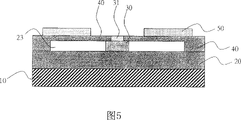
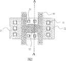
Wherein, the contact layer that this matrix contact zone can be above it not with prerequisite that gate electrode contacts under, build on each position of channel region.Even dig out a perforation to set up matrix contact zone and contact layer thereof in perforation in gate electrode, as shown in Figure 4, it is the structure schematic top plan view of second embodiment of the invention.This thin-film transistor component with matrix contact is to dig out the eight limit type perforation 51 of exposing silicon oxide layer 40 within its gate electrode 50, and, set up matrix contact zone 30 and contact layer 31 thereof in this eight limits type perforation 51, promptly gate electrode 50 zones are for being surrounded on this matrix contact zone 30 and contact layer 31 thereof.Further specify its configuration again, please refer to Fig. 5, it is the generalized section of the structure of second embodiment of the invention, and its hatching is the A '-A line segment among Fig. 4.The relative position of hence one can see that gate electrode 50, matrix contact zone 30 and contact layer 31 thereof.In addition, please refer to Fig. 6, it is the generalized section of the structure of second embodiment of the invention, and its hatching is the B '-B line segment among Fig. 4.Except expressing the relative position of gate electrode 50, matrix contact zone 30 and contact layer 31 thereof, also show the configuration relation of channel region 23, source area 21 and the drain region 22 of polysilicon layer.
In addition, also can form the suitable groove that extends to the channel region top in the edge of gate electrode, and set up matrix contact zone and contact layer thereof in the zone that groove is emptied, as shown in Figure 7, it is the structure schematic top plan view of third embodiment of the invention; Make gate electrode 50 form H shape zone, and set up matrix contact zone and the contact layer thereof that several doping trivalents are led in the groove 52 that extends to channel region 23 tops that it produced, doping pentavalent alms giver's source area 21 and 22 of drain regions is connected to the channel region 23 of this gate electrode below.Relend storehouse and configuration scenario that third embodiment of the invention is described by profile, please refer to Fig. 8, it is the generalized section of the structure of third embodiment of the invention, and its hatching is the A '-A line segment among Fig. 7.It shows the relative position and the configuration of channel region 23, source area 21 and drain region 22 of gate electrode 50, matrix contact zone 30, contact layer 31, the polysilicon layer of the 3rd embodiment.
Wherein, learn that by the foregoing description source area and drain region are adjacent to the contact zone, and the different impurities of being mixed by the matrix contact zone provides matrix to trigger (body-trigger) bias voltage.And electrode grid of the present invention can one of them be made by chromium and aluminium, and above-described method also may be implemented on the P type TFT transistor, to increase its drive current.
Though preferred embodiment of the present invention openly as mentioned above; right its is not in order to limit the present invention; any those skilled in the art; without departing from the spirit and scope of the present invention; when can doing a little change and modification, therefore scope of patent protection of the present invention must be looked the appended claim person of defining of this specification and is as the criterion.
Claims (10)
1. one kind has the thin-film transistor component that matrix contacts, by an insulating body, one polysilicon layer, one insulating barrier and a gate electrode are formed, this polysilicon layer includes a channel region, an one source pole district and a drain region, it is characterized in that: this source area and this drain region are doped with the first suitable impurity and are connected to this channel region, this channel region one end has a matrix contact zone that connects this insulating body and this insulating barrier, this surface, matrix contact zone has a contact layer that runs through this insulating barrier, and, this contact layer does not contact with this gate electrode, this matrix contact zone mixes and second impurity of this source area with these different valence mumbers in drain region, is biased in this insulating body to provide a matrix to trigger.
2. the thin-film transistor component with matrix contact as claimed in claim 1, when wherein this first impurity was a pentavalent alms giver, this second impurity was that a trivalent is led.
3. the thin-film transistor component with matrix contact as claimed in claim 1, wherein this first impurity is that a trivalent is subjected to when main, this second impurity is a pentavalent alms giver.
4. the thin-film transistor component with matrix contact as claimed in claim 1, wherein the edge of this gate electrode forms a groove that extends to this channel region top, and sets up this matrix contact zone and this contact layer in the zone that this groove is emptied.
5. the thin-film transistor component with matrix contact as claimed in claim 1, wherein this electrode grid material is selected from chromium or aluminium.
6. one kind has the thin-film transistor component that matrix contacts, by an insulating body, one polysilicon layer, one insulating barrier and a gate electrode are formed, this polysilicon layer includes a channel region, an one source pole district and a drain region, it is characterized in that: this source area and this drain region are doped with the first suitable impurity and are connected to this channel region, this channel region one end has a matrix contact zone that connects this insulating body and this insulating barrier, this surface, matrix contact zone has a contact layer that runs through this insulating barrier, this contact layer of this matrix contact zone and its top be formed at this gate electrode around an interior zone, and this contact layer does not contact with this gate electrode, this matrix contact zone mixes and second impurity of this source area with these different valence mumbers in drain region, is biased in this insulating body to provide a matrix to trigger.
7. the thin-film transistor component with matrix contact as claimed in claim 6, when wherein this first impurity was a pentavalent alms giver, this second impurity was that a trivalent is led.
8. the thin-film transistor component with matrix contact as claimed in claim 6, wherein this first impurity is that a trivalent is subjected to when main, this second impurity is a pentavalent alms giver.
9. the thin-film transistor component with matrix contact as claimed in claim 6, wherein the edge of this gate electrode forms a groove that extends to this channel region top, and sets up this matrix contact zone and this contact layer in the zone that this groove is emptied.
10. the thin-film transistor component with matrix contact as claimed in claim 6, wherein this electrode grid material is selected from chromium or aluminium.
Priority Applications (1)
| Application Number | Priority Date | Filing Date | Title |
|---|---|---|---|
| CNB031216315A CN1316632C (en) | 2003-03-18 | 2003-03-18 | Thin film transistor assembly with substrate contact |
Applications Claiming Priority (1)
| Application Number | Priority Date | Filing Date | Title |
|---|---|---|---|
| CNB031216315A CN1316632C (en) | 2003-03-18 | 2003-03-18 | Thin film transistor assembly with substrate contact |
Publications (2)
| Publication Number | Publication Date |
|---|---|
| CN1532946A CN1532946A (en) | 2004-09-29 |
| CN1316632C true CN1316632C (en) | 2007-05-16 |
Family
ID=34285760
Family Applications (1)
| Application Number | Title | Priority Date | Filing Date |
|---|---|---|---|
| CNB031216315A Expired - Fee Related CN1316632C (en) | 2003-03-18 | 2003-03-18 | Thin film transistor assembly with substrate contact |
Country Status (1)
| Country | Link |
|---|---|
| CN (1) | CN1316632C (en) |
Families Citing this family (3)
| Publication number | Priority date | Publication date | Assignee | Title |
|---|---|---|---|---|
| US7453122B2 (en) * | 2005-02-08 | 2008-11-18 | Taiwan Semiconductor Manufacturing Co., Ltd. | SOI MOSFET device with reduced polysilicon loading on active area |
| JP4350106B2 (en) | 2005-06-29 | 2009-10-21 | 三星モバイルディスプレイ株式會社 | Flat panel display and driving method thereof |
| CN102664189B (en) * | 2012-05-18 | 2016-08-31 | 中国科学院微电子研究所 | Soi mos transistor |
Citations (3)
| Publication number | Priority date | Publication date | Assignee | Title |
|---|---|---|---|---|
| CN1196832A (en) * | 1996-06-28 | 1998-10-21 | 精工爱普生株式会社 | Thin film transistor, manufacturing method thereof, circuit and liquid crystal display device using same |
| CN1272695A (en) * | 1999-04-15 | 2000-11-08 | 株式会社半导体能源研究所 | Electro-optic devices and electronics |
| JP2002057345A (en) * | 2001-05-14 | 2002-02-22 | Semiconductor Energy Lab Co Ltd | Semiconductor device |
-
2003
- 2003-03-18 CN CNB031216315A patent/CN1316632C/en not_active Expired - Fee Related
Patent Citations (3)
| Publication number | Priority date | Publication date | Assignee | Title |
|---|---|---|---|---|
| CN1196832A (en) * | 1996-06-28 | 1998-10-21 | 精工爱普生株式会社 | Thin film transistor, manufacturing method thereof, circuit and liquid crystal display device using same |
| CN1272695A (en) * | 1999-04-15 | 2000-11-08 | 株式会社半导体能源研究所 | Electro-optic devices and electronics |
| JP2002057345A (en) * | 2001-05-14 | 2002-02-22 | Semiconductor Energy Lab Co Ltd | Semiconductor device |
Also Published As
| Publication number | Publication date |
|---|---|
| CN1532946A (en) | 2004-09-29 |
Similar Documents
| Publication | Publication Date | Title |
|---|---|---|
| EP4297089A1 (en) | Display substrate and display panel | |
| US6310598B1 (en) | Matrix type liquid-crystal display unit | |
| CN102446488B (en) | Semiconductor device | |
| US5536950A (en) | High resolution active matrix LCD cell design | |
| JP3402400B2 (en) | Manufacturing method of semiconductor integrated circuit | |
| CN101320181B (en) | Display device and method of manufacturing the same | |
| WO2020238013A1 (en) | Goa circuit and array substrate | |
| US7038276B2 (en) | TFT with body contacts | |
| CN104779257B (en) | TFT layout structures | |
| CN101789434B (en) | Image display system and manufacturing method thereof | |
| US7256457B2 (en) | Thin-film transistor device, utilizing different types of thin film transistors | |
| JP2005064477A (en) | Thin film transistor in which gate and body are electrically connected, method for manufacturing the same, and display device including the same | |
| CN1316632C (en) | Thin film transistor assembly with substrate contact | |
| JPH02206173A (en) | polycrystalline thin film transistor | |
| JPH0926600A (en) | Liquid crystal display device | |
| JP2997737B2 (en) | Liquid crystal display | |
| JPH0864830A (en) | Active matrix substrate and method of fabrication thereof | |
| JPH08220506A (en) | Liquid crystal display | |
| CN208903642U (en) | Phase inverter and GOA circuit | |
| US11670253B2 (en) | Pixel driving circuit, array substrate and display panel | |
| US8164093B2 (en) | Display device | |
| US6825495B1 (en) | CMOS transistor and CMOS-based device | |
| US20080217619A1 (en) | Thin film transistor and display device | |
| JPH08220505A (en) | Liquid crystal display | |
| US20090045406A1 (en) | Semiconductor device and display device |
Legal Events
| Date | Code | Title | Description |
|---|---|---|---|
| C06 | Publication | ||
| PB01 | Publication | ||
| C10 | Entry into substantive examination | ||
| SE01 | Entry into force of request for substantive examination | ||
| C14 | Grant of patent or utility model | ||
| GR01 | Patent grant | ||
| CF01 | Termination of patent right due to non-payment of annual fee |
Granted publication date: 20070516 Termination date: 20160318 |
|
| CF01 | Termination of patent right due to non-payment of annual fee |