CN1294441C - Optical device - Google Patents
Optical device Download PDFInfo
- Publication number
- CN1294441C CN1294441C CNB038073552A CN03807355A CN1294441C CN 1294441 C CN1294441 C CN 1294441C CN B038073552 A CNB038073552 A CN B038073552A CN 03807355 A CN03807355 A CN 03807355A CN 1294441 C CN1294441 C CN 1294441C
- Authority
- CN
- China
- Prior art keywords
- optical waveguide
- insertion plate
- magnet
- optical
- zone
- Prior art date
- Legal status (The legal status is an assumption and is not a legal conclusion. Google has not performed a legal analysis and makes no representation as to the accuracy of the status listed.)
- Expired - Fee Related
Links
Images


Classifications
-
- G—PHYSICS
- G02—OPTICS
- G02B—OPTICAL ELEMENTS, SYSTEMS OR APPARATUS
- G02B26/00—Optical devices or arrangements for the control of light using movable or deformable optical elements
- G02B26/08—Optical devices or arrangements for the control of light using movable or deformable optical elements for controlling the direction of light
-
- G—PHYSICS
- G02—OPTICS
- G02B—OPTICAL ELEMENTS, SYSTEMS OR APPARATUS
- G02B6/00—Light guides; Structural details of arrangements comprising light guides and other optical elements, e.g. couplings
- G02B6/24—Coupling light guides
- G02B6/26—Optical coupling means
- G02B6/35—Optical coupling means having switching means
- G02B6/3564—Mechanical details of the actuation mechanism associated with the moving element or mounting mechanism details
- G02B6/3568—Mechanical details of the actuation mechanism associated with the moving element or mounting mechanism details characterised by the actuating force
- G02B6/3572—Magnetic force
-
- G—PHYSICS
- G02—OPTICS
- G02B—OPTICAL ELEMENTS, SYSTEMS OR APPARATUS
- G02B26/00—Optical devices or arrangements for the control of light using movable or deformable optical elements
-
- G—PHYSICS
- G02—OPTICS
- G02B—OPTICAL ELEMENTS, SYSTEMS OR APPARATUS
- G02B6/00—Light guides; Structural details of arrangements comprising light guides and other optical elements, e.g. couplings
- G02B6/24—Coupling light guides
- G02B6/26—Optical coupling means
- G02B6/35—Optical coupling means having switching means
- G02B6/351—Optical coupling means having switching means involving stationary waveguides with moving interposed optical elements
- G02B6/3512—Optical coupling means having switching means involving stationary waveguides with moving interposed optical elements the optical element being reflective, e.g. mirror
- G02B6/3514—Optical coupling means having switching means involving stationary waveguides with moving interposed optical elements the optical element being reflective, e.g. mirror the reflective optical element moving along a line so as to translate into and out of the beam path, i.e. across the beam path
-
- G—PHYSICS
- G02—OPTICS
- G02B—OPTICAL ELEMENTS, SYSTEMS OR APPARATUS
- G02B6/00—Light guides; Structural details of arrangements comprising light guides and other optical elements, e.g. couplings
- G02B6/24—Coupling light guides
- G02B6/26—Optical coupling means
- G02B6/35—Optical coupling means having switching means
- G02B6/351—Optical coupling means having switching means involving stationary waveguides with moving interposed optical elements
- G02B6/353—Optical coupling means having switching means involving stationary waveguides with moving interposed optical elements the optical element being a shutter, baffle, beam dump or opaque element
-
- G—PHYSICS
- G02—OPTICS
- G02B—OPTICAL ELEMENTS, SYSTEMS OR APPARATUS
- G02B6/00—Light guides; Structural details of arrangements comprising light guides and other optical elements, e.g. couplings
- G02B6/24—Coupling light guides
- G02B6/26—Optical coupling means
- G02B6/35—Optical coupling means having switching means
- G02B6/354—Switching arrangements, i.e. number of input/output ports and interconnection types
- G02B6/3544—2D constellations, i.e. with switching elements and switched beams located in a plane
- G02B6/3548—1xN switch, i.e. one input and a selectable single output of N possible outputs
-
- G—PHYSICS
- G02—OPTICS
- G02B—OPTICAL ELEMENTS, SYSTEMS OR APPARATUS
- G02B6/00—Light guides; Structural details of arrangements comprising light guides and other optical elements, e.g. couplings
- G02B6/24—Coupling light guides
- G02B6/26—Optical coupling means
- G02B6/35—Optical coupling means having switching means
- G02B6/3564—Mechanical details of the actuation mechanism associated with the moving element or mounting mechanism details
- G02B6/3566—Mechanical details of the actuation mechanism associated with the moving element or mounting mechanism details involving bending a beam, e.g. with cantilever
-
- G—PHYSICS
- G02—OPTICS
- G02B—OPTICAL ELEMENTS, SYSTEMS OR APPARATUS
- G02B6/00—Light guides; Structural details of arrangements comprising light guides and other optical elements, e.g. couplings
- G02B6/24—Coupling light guides
- G02B6/26—Optical coupling means
- G02B6/35—Optical coupling means having switching means
- G02B6/3564—Mechanical details of the actuation mechanism associated with the moving element or mounting mechanism details
- G02B6/3584—Mechanical details of the actuation mechanism associated with the moving element or mounting mechanism details constructional details of an associated actuator having a MEMS construction, i.e. constructed using semiconductor technology such as etching
-
- G—PHYSICS
- G02—OPTICS
- G02B—OPTICAL ELEMENTS, SYSTEMS OR APPARATUS
- G02B6/00—Light guides; Structural details of arrangements comprising light guides and other optical elements, e.g. couplings
- G02B6/24—Coupling light guides
- G02B6/26—Optical coupling means
- G02B6/35—Optical coupling means having switching means
- G02B6/3596—With planar waveguide arrangement, i.e. in a substrate, regardless if actuating mechanism is outside the substrate
Abstract
An optical device is configured such that an insertion plate is held by a flat cantilever having electric wiring, and the flat magnet is placed in such a manner that the magnet faces a surface of the cantilever opposite to the other surface of the cantilever facing an optical waveguide, and that the current flowing through the electric wiring is controlled in this state so that the Lorentz force caused by the interaction between the current and the magnetic field displaces the cantilever to drive the insertion plate, and to insert or remove the insertion plate into or out of the slit provided in the optical waveguide to switch the optical path of signal light or to adjust the quantity of an optical beam.
Description
Technical area
The present invention relates to optical devices, more particularly, relate to the optical devices such as optical-waveguide-type matrix switch and variable attenuator that are used for driving mirror plate or shadow shield action by magnet.
Background technology
In the prior art, known have such photoswitch, wherein make the shield action of in the way of the optical waveguide that constitutes photoswitch, disposing, make light beam from optical waveguide be interdicted or pass through, open flat 05-257069 communique and spy the spy and open and put down in writing its concrete formation in the flat 02-131210 communique.Below, will have photoswitch that the spy opens the formation of being put down in writing in the flat 05-257069 communique as prior art A, have photoswitch that the spy opens the formation of being put down in writing in the flat 02-131210 communique as prior art B, prior art is described.
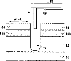
Figure 12 is a planimetric map, is used for illustrating the formation of the photoswitch that prior art A discloses.This photoswitch has: in the inside 113 of ditch portion 112, be provided with, along ditch direction glass sheet 115 movably, 112 crosscuts of described ditch portion are formed at the optical waveguide 111 on the substrate; Be positioned at glass sheet 115 two ends, be communicated with ditch portion 112, the liquid metals that maintains liquid metals (mercury) 116 in inside keeps ditch 117; Make liquid metals keep the electrode 118A that flows through electric current respectively and B and the 119A and the B of the ditch 117 inner liquid metals 116 that keep; And unshowned and current flowing direction vertically applies the magnetic field applying unit in magnetic field.
Therefore, when having electric current to flow through in the liquid metals 116, apply magnetic field in the direction vertical (Z direction) with the flow direction (directions X) of this electric current, liquid metals 116 is applied Lorentz (Lorentz) power, make it in liquid keeps ditch, to move to the Y direction, mobile glass sheet makes the speculum 114 blocking optical waveguides 111 on the part that is arranged at glass sheet.Perhaps, make direction of current flow opposite, thereby speculum 114 is kept out of the way out from optical waveguide, thereby the input light by optical waveguide 111 is passed through with above-mentioned situation.Like this, flow through the sense of current of liquid metals 116, constitute the photoswitch that makes the light propagated in the optical waveguide 111 interdict/pass through by control.Like this in the photoswitch of Gou Chenging, be used for magnet (not shown) that above-below direction (Z direction) at substrate generates magnetic field be disposed at substrate about.
Figure 13 is the schematic cross-section of the formation of the photoswitch that is used to illustrate that prior art B is disclosed, the displacement plate that 121 expressions are made by conductive material, 122 expressions be arranged at displacement plate 121 front end, the light of propagation is interdicted/element (element) that passes through, 124 express support for the insulation course of the rear end side of displacement plate 121,125 expression switches, 126 expressions are power supplys, 128 expression optical waveguides, the gap that is provided with in the 127 expression optical waveguides 128, the 123rd, the conductive material layer that on the surface of optical waveguide 128, is provided with along the optical waveguide direction.
In the photoswitch of structure shown in Figure 13, apply voltage, by electrostatic force, element 122 is moved, the photoswitch action that makes light interdict/pass through in the direction (above-below direction of paper) perpendicular to substrate in displacement plate 121 and 123 effects of conductive material layer.
Yet, in the formation of the photoswitch of described prior art A, for configuration in optical waveguide makes the drive part that keeps ditch, electrode etc. to constitute by liquid metals of moving part action, need certain space, make the one-piece construction of the photoswitch that comprises drive part become big.Particularly, when a plurality of switching elements were the array-like configuration on same substrate, described drive division became the integrated obstacle of high density of switching element with the space.
In addition, in the formation of the photoswitch of described prior art B, the direction of motion of shield is vertical with substrate, and it is configured to the space contact optical waveguide from the optical waveguide top, thereby need not be in optical waveguide configuration driven mechanism, this point can be described as the integrated formation of high density that is suitable for optical waveguide.But this formation utilizes electrostatic force as driving force, in order to drive, needs high-tension electricity, thereby its peripheral electronic loop, device are maximized, and the miniaturization of optical switch device integral body is restricted.
Therefore, have both as " Lorentz force drivings " and " movable member vertical moving " of the advantage of above-mentioned prior art structure the two type of drive if adopt, then can realize simultaneously the high density of optical waveguide integrated with the miniaturization of installing.But, the formation of the photoswitch of this structure (optical devices) or the unknown.
Summary of the invention
The present invention be directed to such problem and propose, its purpose is, provides to be suitable for miniaturization and the integrated optical devices (photoswitch) of high density, makes the shield of the blocking carry out light/by operation move by Lorentz force in the vertical direction of substrate.
The objective of the invention is, a kind of optical devices are provided, it has a slit (slit) at least, described slit is located at the desired locations place of the optical waveguide of the polygon plane shape that is provided with on the substrate, insert plate and move up and down this slit of turnover and carry out the switching of light path of flashlight or the adjustment of the light quantity of light beam by making, these optical devices comprise: insert the plate holding device, be used to support described insertion plate; Be formed on the electric wiring on the described insertion plate holding device; With tabular magnet, it is fixedly located in a surface towards described insertion plate holding device, a surface of described insertion plate holding device is and surface towards the surface opposite of described optical waveguide that described magnet is configured such that magnetic field is applied on the described electric wiring of at least a portion.By separate the interactional Lorentz force in the magnetic field that the described magnet that forms produces based on the electric current that flows in the described electric wiring with described insertion plate, mobile described insertion plate holding device, thus drive described insertion plate.
In such optical devices, the size of described magnet and shape form and can make the projected image that projects on the described optical waveguide in vertical direction be accommodated in this light wave guide face.
And described optical devices constitute and magnet configuration are become to make to project to the bearing of trend of straight line portion of the projected outline on the described optical waveguide from vertical direction non-orthogonal with the magnetic direction of this magnet generation.
Description of drawings
Fig. 1 is the planimetric map that the 1st configuration example of the optical waveguide that is equipped with in the optical devices of the present invention is described;
Fig. 2 is the sectional view of the relation between the insertion plate that is provided with in the optical waveguide that has of explanation optical devices of the present invention and slit portion divide;
Fig. 3 is the slit part of the optical waveguide that has of explanation optical devices of the present invention and the sectional view that inserts near the 1st configuration example the plate;
Fig. 4 is used to illustrate that magnet shown in Figure 3 produces the situation of the magnetic line of force;
Fig. 5 is used to illustrate the optical waveguide of whole zone to the formation of the outside of magnet expansion;
Fig. 6 is the planimetric map of optical waveguide, and the shape of the magnet that has in the optical waveguide of optical devices of the present invention is described;
Fig. 7 is the planimetric map of optical waveguide, and other shapes of the magnet that has in the optical waveguide of optical devices of the present invention are described;
Fig. 8 is the planimetric map of configuration example of the optical waveguide of explanation optical devices of the present invention;
Fig. 9 is the schematic cross-section of the relation between the insertion plate that has and slit portion divide in the optical waveguide of explanation optical devices of the present invention;
Figure 10 A and Figure 10 B are the upward views of insertion plate shown in Figure 9 and cantilever (cantilever);
Figure 11 be explanation optical devices of the present invention optical waveguide slit part and insert near the sectional view of the configuration example the plate;
Figure 12 is the planimetric map of the formation of the photoswitch that disclosed of explanation prior art A;
Figure 13 is the schematic cross-section of the formation of the photoswitch that disclosed of explanation prior art B.
Embodiment of the present invention
Below, embodiments of the present invention are described with reference to the accompanying drawings.
(embodiment 1)
Fig. 1 is the planimetric map of the 1st configuration example of explanation optical devices of the present invention, and the optical waveguide 72 that these optical devices had is arranged on the support matrices 71 of rectangular light waveguide, and five waveguide regions of same-action constitute by having not respectively.
Zone 1 (73) is the zone that comprises the light signal input side connection end face of the optical fiber with any amount, zone 4 (76) is to comprise the zone that optical fiber connects end face, is equivalent to from the zone 1 (73) input, by in the slit part S and the outgoing side of the light signal of directly coming in.Zone 3 (75) comprises the zone that is equivalent to from the zone 1 (73) input, connects end face at the optical fiber of the outgoing side of the light signal of slit part S internal reflection.Zone 5 (77) is not comprise the zone of the output of optical waveguide with optical fiber link face.
In the rectangular area 2 (74) that these zones surrounded, be provided with slit part S, among this slit part S, the route control of flashlight is carried out in the plug of the insertion plate M by field drives.Therefore, in zone 2 (74),, need apply necessary magnetic field in order to drive the insertion plate.
Among Fig. 1, be used as the light beam I of input light
1And I
2The state of the representational optical waveguide in the illustration input waveguide zone 1 (73).For light beam I
1, because insert plate M in slit part S, input beam I
1Through inserting the plate M reflection, output belongs to the optical fiber that reflects outgoing side and connects the reflected light R that uses zone 3 (75).And to light beam I
2, owing to do not insert plate M, light beam I in the slit part S
2Directly enter by slit S inside, to exporting the light T that sees through as the zone 4 (76) of output light optical fiber join domain.
Inserting by magnetic field and current drives under the situation of plate M, the direction of magnetic field B is with respect to most effective when angulation is the right angle near the parallel face in the being seen slit of last direction cross section shown in Figure 1 (or insertion plate in slit and it formed movement locus face).Therefore, the direction of distributed magnet, the direction that makes magnetic field B is direction of arrow B shown in dotted lines in Figure 1.Insert plate M and fixedly connected, insert plate M and be driven in mode with the cantilever interlock with not shown cantilever.This driving is by the control of inserting the electric current that flows in the electric wiring that is provided with on plate M or the insertion plate M cantilever is nearby carried out.
Fig. 2 is the schematic cross-section of the relation of the insertion plate that is provided with in explanation the optical waveguide that optical devices of the present invention had and slit part.Be laminated with on the substrate 81 and be formed with input optical fibre sidelight waveguide core 83a and output optical fibre sidelight waveguide core 83b on clad (clad) 82, the clad 82, be laminated with clad 84 above these waveguide cores, thereby constitute the part of optical waveguide, in this part, form slit part S.Insert plate M and be fixed on the cantilever 85, be subjected at least in slit part S, to plug being arranged on the cantilever 85 and on direction, having the current drives that flows in the electric wiring 86 of certain-length perpendicular to paper.
Act on the magnetic field of inserting on the plate M and have the component parallel with paper, this magnetic-field component acts on the part of the electric wiring 86 of the composition with the right angle orientation in the paper, when in the electric wiring 86 electric current being arranged, according to the Fleming rule, corresponding to the flow direction of electric current, to cantilever 85 apply upward to or the Lorentz force that drives of direction down.The magnetic direction that acts on the Lorentz force maximum of cantilever 85 is and the vertical direction of moving direction of inserting plate M.
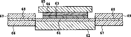
Fig. 3 is the slit part of the optical waveguide that has of explanation optical devices of the present invention and the sectional view that inserts plate the 1st configuration example nearby, form optical waveguide 91 on the supporting substrate 92 of optical waveguide, above this optical waveguide 91, dispose MEMS (MEMS:micro-electromechanical system, microelectromechanical-systems) supporting substrate 94 and magnet 95.Described MEMS supporting substrate 94 has the MEMS that accommodates insertion plate driving mechanism MEMS and accommodates zone 93.
Fig. 4 is used to illustrate that magnet shown in Figure 3 produces the figure of the appearance of the magnetic line of force, for ease of understanding, has only represented the magnetic line of force to optical waveguide 101 sides.Because the magnetic line of force is loose more more away from magnet 102, magnetic force is just weak more, among Fig. 3 MEMS is accommodated zone 93 and is positioned as close to magnet 95 installations, and the effect of magnet is brought into play in expectation effectively, drives to insert plate.
That is to say that the optical devices of present embodiment comprise: tabular insertion plate holding member, it has electric wiring, is used for keeping inserting plate; Tabular magnet, it is towards a surface of inserting the plate holding member, and a surface of this insertion plate holding member is and surface opposite surface towards optical waveguide one side.Interactional Lorentz force by the magnetic field that produces based on the electric current that flows in the electric wiring and magnet moves and inserts the plate holding member, inserts plate thereby drive.
Fig. 5 is used to illustrate to have the optical waveguide of whole area extension to the formation in the magnet outside.
(embodiment 2)
The optical devices of the present invention of the foregoing description 1 make the type of drive of the insertion plate of " Lorentz force driving " and " vertical moving of movable member " the two establishment except having adopted, the high density that makes optical waveguide is integrated and thereby the miniaturization of device can realize having outside in the past the unexistent advantage of formation simultaneously, also has following improvement.
The first, in Fig. 3, when the position on decision optical waveguide 91 and input side and output side of optical fiber 96,97 above-below direction at vertical drawing concerns, at first, with the center of the fiber cores 98 of the input side optical fibers 96 of light signal and output side of optical fiber 97 with mechanically fixing after the end face of optical waveguide 91 is aimed at accurately.Like this, the radius of the optical fibre packages coating 99 of the arranged outside of the fiber cores 98 of the optical fiber 96,97 that is connected with the input and output end face of optical waveguide 91 is according to present standard, be hundred tens of microns, tens of microns of the thickness of the sandwich layer of this value ratio formation optical waveguide 91 and the thickness sum of clad are big, thereby the upper end of optical fibre packages coating 99 is positioned at the top of the upper end of optical waveguide 91.
Therefore, the approaching potential range of the end face of the bottom surface of magnet 95 and optical waveguide 91 is limited by the difference of the thickness sum of the thickness of the radius of optical fibre packages coating 99 and the sandwich layer that constitutes optical waveguide 91 and clad, thereby becomes magnet 95 to optical waveguide 91 near the obstacles that effectively utilize magnetic force.
The second, in order to address this problem, as shown in Figure 5 the whole zone (regional 1+2+3+4+5) of optical waveguide is expanded to the outside in magnet zone (zone 10), then optical waveguide can be had to 4 times the area in zone 2 as the configuring area of the slit of the basic function of bearing optical devices, has limited the reducing of area of chip of light waveguide.
Therefore, in the present embodiment, to can effectively utilizing magnetic force, and the optical devices of the present invention that the area of chip of light waveguide is reduced describe.
Fig. 6 is the planimetric map of the optical waveguide of the shape example of the magnet that has in the optical waveguide of explanation optical devices of the present invention, and this optical waveguide 12 is arranged on the support matrices 11 of optical waveguide of rectangle, and five waveguide regions of same-action constitute by rising not respectively.
Zone 1 (13) is that the light signal input side that comprises the optical fiber with any amount connects end face, and zone 4 (16) is the zone that the optical fiber that comprises the outgoing side of the light signal that is equivalent to 1 (13) input from the zone and directly comes in connects end face.Zone 3 (15) is to comprise to be equivalent to from the zone 1 (13) input, to connect the zone of end face through the optical fiber of the outgoing side of the light signal of slit portion sub reflector, and zone 5 (17) is not comprise the zone of the output of optical waveguide with optical fiber link face.
In the rectangular area 2 (14) that these zones surrounded, be provided with the slit part.In this slit part, come the route of control signal light by plug by the insertion plate of field drives.Therefore, in the zone 2 (14),, be provided with the magnet 18 in necessary generation magnetic field in order to drive the insertion plate.
This magnet 18 have with four angles of rectangle (a, b, c, d) Qie Chu octagonal shape, its shape and the size it can be accommodated in the zone of optical waveguide 12 from the projected image that vertical direction projects on the optical waveguide 12.Like this, the magnetic field intensity in the whole zone in zone 2 (14) is even, and the also comparable optical waveguide in the past of the whole area of optical waveguide 12 is little.
Fig. 7 is the optical waveguide planimetric map that other shape magnet that have in the optical waveguide of optical devices of the present invention are described, this optical waveguide 22 is arranged on the rectangular light waveguide support matrices 21, and five waveguide regions of same-action constitute by rising not respectively.
Zone 1 (23) is the zone that the light signal input side that comprises the optical fiber with any amount connects end face, and zone 4 (26) is the zone that the optical fiber that comprises the outgoing side of the light signal that is equivalent to 1 (23) input from the zone and directly enters connects end face.Zone 3 (25) is to comprise to be equivalent to be entered and connected the zone of end face at the optical fiber of the outgoing side of the light signal of slit portion sub reflector by zone 1 (23), and zone 5 (27) is not comprise the zone of the output of optical waveguide with optical fiber link face.
In the rectangular area 2 (24) that these zones surrounded, be provided with the slit part, the route control of flashlight is carried out in the plug of the insertion plate by field drives in this slit part.Therefore, in the zone 2 (24),, be provided with the magnet 28 in necessary generation magnetic field in order to drive the insertion plate.
It is non-orthogonal that the configuration of this magnet 28 should make it project to the magnetic direction that bearing of trend and the magnet of the straight line portion of the projected outline on the optical waveguide produces (this figure for and insert the vertical direction of plate) from vertical direction, and its shape is the rectangle of the minimum area of overlay area 2 (24).By the shape of magnet 28 is set like this, can make the magnetic field intensity in 2 (24) whole zones, zone even, thereby the whole area of optical waveguide 22 is dwindled greatly, with the optical waveguide of formation shown in Figure 1 relatively, can be contracted to about 1/4.
In the example shown in Figure 7, being shaped as of magnet 28 be the simplest, make and be easy to rectangle, and its shape not only is confined to this, so long as the direction in magnetic field is with to insert plate vertical, the end face of magnet cover slit shape partly can, for example rhombus etc. also can.
Fig. 8 is the planimetric map of configuration example of the optical waveguide of explanation optical devices of the present invention, and this optical waveguide 32 is arranged on the support matrices 31 of optical waveguide of rectangle, and five waveguide regions of same-action constitute by rising not respectively.
Zone 1 (33) is to comprise the zone that the light signal input side with any amount optical fiber connects end face, and zone 4 (36) is to comprise to be equivalent to enter from zone 1 (33) and the optical fiber of outgoing side by the light signal of directly coming in the slit part S connects the zone of end face.Zone 3 (35) is to comprise to be equivalent to be entered and connected the zone of end face at the optical fiber of the outgoing side of the light signal of slit part S internal reflection by zone 1 (33), and zone 5 (37) is not comprise the zone of the output of optical waveguide with optical fiber link face.
In the rectangular area 2 (34) that these zones surrounded, be provided with slit part S, the route control of flashlight is carried out in the plug of the insertion plate M by field drives among this slit part S.Therefore, in the zone 2 (34), insert plate M, need apply necessary magnetic field in order to drive.
Among Fig. 8, be used as the light beam I of input light
1And I
2The state of representing the representational optical waveguide in the input waveguide zone 1 (33) for example.For light beam I
1, because insert plate M in slit part S, input beam I
1Through inserting the plate M reflection, output belongs to the optical fiber that reflects outgoing side and connects the reflected light R that uses zone 3 (35).And to light beam I
2, owing to do not insert plate M in the slit part S, light beam 2 directly enters by slit S inside, passes through light T to zone 4 (36) outputs as the output optical fibre join domain.
Inserting under the situation of plate M by magnetic field and current drives, the direction of magnetic field B with as shown in Figure 8 from the parallel face in the cross section of the being seen slit in top (or insert plate in slit and its formed movement locus face nearby) angulation is most effective under the situation at right angle, therefore, the direction of distributed magnet, the direction that makes magnetic field B is the direction of arrow shown in dotted lines in Figure 8.Insert plate M and fixedly connected, insert plate M and cantilever interlock and drive with not shown cantilever.This driving is by the control of inserting plate M or being arranged on the electric current that flows in the electric wiring that inserts plate M cantilever is nearby carried out.
Fig. 9 is the schematic cross-section of the relation between the insertion plate that has and slit portion divide in the optical waveguide of explanation optical devices of the present invention.Be laminated with clad 42 on the substrate 41, be formed with input optical fibre sidelight waveguide core 43a and output optical fibre sidelight waveguide core 43b on the clad 42, be laminated with clad 44 above these waveguide cores, thus the part of the optical waveguide that constitutes.On this part, form slit part S.Insert plate M and be fixed on the cantilever 45, be subjected to be arranged on the cantilever 45 and on direction, having the current drives that flows in the electric wiring 46 of certain-length at least, thereby in slit part S, plug perpendicular to paper.
Act on the magnetic field of inserting plate M and have the component parallel with paper, this magnetic-field component acts on the part of the electric wiring 46 with composition of right angle orientation on the paper, when in the electric wiring 46 electric current being arranged, according to the Fleming rule, corresponding to the flow direction of electric current, to cantilever 45 apply upward to or the Lorentz force that drives of direction down.The magnetic direction that makes the Lorentz force maximum that acts on cantilever 45 is and the vertical direction of moving direction of inserting plate M.
Here, be that the amount that the vector product in the electric current that flows in by the wiring on the cantilever and magnetic field is carried out line integral along wiring obtains to the Lorentz force that cantilever applies.It is very important that wiring does not form closed curve.For example, such shown in Figure 10 A and Figure 10 B as described later, tetragonal three limits are positioned on the moving part of cantilever, there is the fixed part of cantilever on the right side that is equivalent to one side of opening of Figure 10 A and 10B, wiring is drawn to the outside from the fixed part at place, and its necessary condition is that the outside does not have magnetic field or magnetic field very low.
Figure 10 A and Figure 10 B are the upward views of insertion plate shown in Figure 9 and cantilever.Figure 10 A is the bearing of trend that inserts plate 51a and the cantilever 52a planimetric map when meeting at right angles installation.At this moment, the direction in magnetic field is positioned at paper, and, under the situation parallel, as the Lorentz force maximum of line integral with the length direction of cantilever 52b.In addition, Figure 10 B is the length direction that inserts plate 51b and the cantilever 52b planimetric map when installing abreast.
Insert fixing free-ended fore-end that is held in cantilever 52a, 52b under the free end side pre-curved state that constitutes so bimetallic single-cantilever of plate 51a, 51b.The effect of the Lorentz force that produces by the electric current that flows among the electric wiring 53a, the 53b that are provided with among cantilever 52a, the 52b increases or reduces the amount of bow of cantilever, makes and inserts the plate motion.
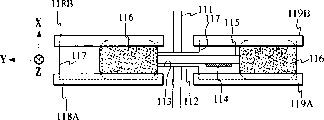
Figure 11 be explanation optical devices of the present invention optical waveguide slit part and insert near the sectional view of the configuration example the plate.On the supporting substrate 62 of optical waveguide, form optical waveguide 61.Above the optical waveguide 61, dispose MEMS supporting substrate 64 and magnet 65 at this, described MEMS supporting substrate 64 has the MEMS that accommodates insertion plate driving mechanism (MEMS) and accommodates zone 63.
The size of magnet 65 and shape form the projected image that projects on the optical waveguide 61 from vertical direction is accommodated in the face of optical waveguide 61, and its material preferably uses the magnet based on Nd-Fe-B, but also is not limited thereto.
When definite optical waveguide 61 and the input side with optical fibre packages coating 69 and output side of optical fiber 66,67 concern in the position of vertical page, at first, with the center of the fiber cores 68 of the input side optical fibers 66 of light signal and output side of optical fiber 67 with after the end face of optical waveguide 61 is aimed at accurately, carry out mechanical fixation, to form optical element.
In addition, among Figure 11, describe the formation that supporting substrate 62 and optical fiber directly engage, but be not limited to such formation, also can connect supporting substrate 62 and optical fiber by the tie point that forms by stiffening plate that on guided wave terminal face, is provided with for reinforced company's contact surface etc.
The possibility of utilizing on the industry
As discussed above, the formation of Optical devices of the present invention (photoswitch) will be inserted Entering plate remains in the tabular cantilever with electric wiring, with the table of the fiber waveguide side of this cantilever Mutually in the face of the tabular magnet of ground configuration, under this state, control electric cloth on the surface of face opposition side The electric current that flows in the line, by the interactional Lorentz force based on electric current and magnetic field, mobile outstanding Arm drives and inserts plate, by inserting the plate knee-action, makes it debouch arrange in the fiber waveguide narrow Seam comes the light path of switching signal light or the light quantity of adjustment light beam. In addition, can have can for this magnet To project to projected image on the fiber waveguide from vertical direction and be accommodated in shape in the light wave guide face and big Little, perhaps its shape and size are so that project to the straight of projected outline on the fiber waveguide from vertical direction The magnetic direction that the bearing of trend of line part and this magnet produce is non-orthogonal.
By such formation, the shield that is used for the blocking of light/by operation utilizes the vertical of substrate The Lorentz force of direction moves, and the optics that is suitable for miniaturization and high-density integrated can be provided Device (photoswitch).
Claims (3)
1. optical devices, it has a slit at least, described slit is located at the desired locations place of the optical waveguide of the polygon plane shape that is provided with on the substrate, described optical devices come the light path of switching signal light or carry out the adjustment of light beam light quantity by making the insertion plate move up and down the described slit of turnover, it is characterized in that, comprising:
Tabular insertion plate holding device is used to support described insertion plate;
Be formed on the electric wiring on the described insertion plate holding device; With
Tabular magnet, it is fixedly located on a surface of described insertion plate holding device, this surface of described insertion plate holding device is and surface towards the surface opposite of described optical waveguide that described magnet is configured such that magnetic field is applied on the described electric wiring of at least a portion
The utilization of wherein said insertion plate holding device is moved based on electric current in the described electric wiring with Lorentz force that described insertion plate separates the interaction generation in the magnetic field that described magnet produces that forms, thereby drives described insertion plate.
2. optical devices as claimed in claim 1 is characterized in that, the size of described magnet and shape form the image that projects on the described optical waveguide from vertical direction is accommodated in this light wave guide face.
3. optical devices as claimed in claim 1 is characterized in that, the configuration of described magnet makes that to project to the bearing of trend of straight line portion of the projected outline on the described optical waveguide from vertical direction non-orthogonal with the magnetic direction of this magnet generation.
Applications Claiming Priority (4)
| Application Number | Priority Date | Filing Date | Title |
|---|---|---|---|
| JP91405/2002 | 2002-03-28 | ||
| JP2002091405 | 2002-03-28 | ||
| JP2003081362A JP2004004649A (en) | 2002-03-28 | 2003-03-24 | Optical device |
| JP81362/2003 | 2003-03-24 |
Publications (2)
| Publication Number | Publication Date |
|---|---|
| CN1643433A CN1643433A (en) | 2005-07-20 |
| CN1294441C true CN1294441C (en) | 2007-01-10 |
Family
ID=28677554
Family Applications (1)
| Application Number | Title | Priority Date | Filing Date |
|---|---|---|---|
| CNB038073552A Expired - Fee Related CN1294441C (en) | 2002-03-28 | 2003-03-27 | Optical device |
Country Status (7)
| Country | Link |
|---|---|
| US (1) | US7082251B2 (en) |
| EP (1) | EP1489450A4 (en) |
| JP (1) | JP2004004649A (en) |
| KR (1) | KR100603144B1 (en) |
| CN (1) | CN1294441C (en) |
| AU (1) | AU2003220849A1 (en) |
| WO (1) | WO2003083550A1 (en) |
Families Citing this family (5)
| Publication number | Priority date | Publication date | Assignee | Title |
|---|---|---|---|---|
| KR100693415B1 (en) * | 2004-12-14 | 2007-03-12 | 엘지전자 주식회사 | Fading shutter device for the projention television |
| DE112008003660T5 (en) | 2008-01-31 | 2010-12-30 | Hewlett-Packard Development Co., L.P., Houston | Optical taps for circuit boards mounted optical waveguides |
| CN102089638A (en) * | 2009-09-02 | 2011-06-08 | 康达尔芯片设计有限公司 | A mems stress concentrating structure for MEMS sensors |
| US9075566B2 (en) | 2012-03-02 | 2015-07-07 | Microsoft Technoogy Licensing, LLC | Flexible hinge spine |
| KR102373724B1 (en) * | 2019-11-13 | 2022-03-14 | 한국과학기술원 | Optical switching element and system using movable optical waveguide by electromagnetic force |
Citations (6)
| Publication number | Priority date | Publication date | Assignee | Title |
|---|---|---|---|---|
| JPH05257069A (en) * | 1992-03-16 | 1993-10-08 | Nippon Telegr & Teleph Corp <Ntt> | Optical switch |
| JPH11119123A (en) * | 1997-10-20 | 1999-04-30 | Tdk Corp | Optical switch and manufacture thereof |
| US6219472B1 (en) * | 1997-02-17 | 2001-04-17 | Hitachi, Ltd. | Optical switch, method of manufacturing same, and optical communication equipment using the same |
| JP2001264652A (en) * | 2000-03-17 | 2001-09-26 | Mitsubishi Electric Corp | Optical switch |
| CN1324453A (en) * | 1998-10-23 | 2001-11-28 | 康宁股份有限公司 | Fluid-encapsulated MEMS optical switch |
| US6360036B1 (en) * | 2000-01-14 | 2002-03-19 | Corning Incorporated | MEMS optical switch and method of manufacture |
Family Cites Families (12)
| Publication number | Priority date | Publication date | Assignee | Title |
|---|---|---|---|---|
| JPS5794702A (en) * | 1980-12-04 | 1982-06-12 | Oval Eng Co Ltd | Optical lead switch |
| FR2618914B1 (en) * | 1987-07-31 | 1991-12-06 | Alain Souloumiac | IMPROVEMENTS TO OPTOMAGNETIC SWITCHES |
| JPH02131210A (en) * | 1988-11-11 | 1990-05-21 | Nippon Telegr & Teleph Corp <Ntt> | Optical waveguide switch |
| FR2660444B1 (en) * | 1990-03-27 | 1992-10-16 | Commissariat Energie Atomique | INTEGRATED MULTI - CHANNEL OPTICAL SWITCHING SYSTEM AND SWITCHING MANUFACTURING METHOD. |
| US6301425B1 (en) * | 1999-02-22 | 2001-10-09 | Agere Systems Optoelectronics Guardian Corp. | Magnetically tunable optical attenuator and method of attenuating signals |
| US6496612B1 (en) * | 1999-09-23 | 2002-12-17 | Arizona State University | Electronically latching micro-magnetic switches and method of operating same |
| US6493482B1 (en) * | 1999-11-23 | 2002-12-10 | L3 Optics, Inc. | Optical switch having a planar waveguide and a shutter actuator |
| US20010051014A1 (en) * | 2000-03-24 | 2001-12-13 | Behrang Behin | Optical switch employing biased rotatable combdrive devices and methods |
| JP2002023069A (en) * | 2000-07-12 | 2002-01-23 | Sumitomo Electric Ind Ltd | Optical switch |
| TW531669B (en) * | 2000-09-15 | 2003-05-11 | Ibm | Optical devices |
| JP2003035875A (en) * | 2001-07-24 | 2003-02-07 | Hitachi Ltd | Optical switch |
| JP4089215B2 (en) | 2001-09-17 | 2008-05-28 | 株式会社ニコン | Microactuator, and microactuator device, optical switch, and optical switch array using the same |
-
2003
- 2003-03-24 JP JP2003081362A patent/JP2004004649A/en active Pending
- 2003-03-27 AU AU2003220849A patent/AU2003220849A1/en not_active Abandoned
- 2003-03-27 WO PCT/JP2003/003877 patent/WO2003083550A1/en active IP Right Grant
- 2003-03-27 KR KR1020047014765A patent/KR100603144B1/en not_active IP Right Cessation
- 2003-03-27 US US10/509,018 patent/US7082251B2/en not_active Expired - Lifetime
- 2003-03-27 CN CNB038073552A patent/CN1294441C/en not_active Expired - Fee Related
- 2003-03-27 EP EP03715545A patent/EP1489450A4/en not_active Withdrawn
Patent Citations (6)
| Publication number | Priority date | Publication date | Assignee | Title |
|---|---|---|---|---|
| JPH05257069A (en) * | 1992-03-16 | 1993-10-08 | Nippon Telegr & Teleph Corp <Ntt> | Optical switch |
| US6219472B1 (en) * | 1997-02-17 | 2001-04-17 | Hitachi, Ltd. | Optical switch, method of manufacturing same, and optical communication equipment using the same |
| JPH11119123A (en) * | 1997-10-20 | 1999-04-30 | Tdk Corp | Optical switch and manufacture thereof |
| CN1324453A (en) * | 1998-10-23 | 2001-11-28 | 康宁股份有限公司 | Fluid-encapsulated MEMS optical switch |
| US6360036B1 (en) * | 2000-01-14 | 2002-03-19 | Corning Incorporated | MEMS optical switch and method of manufacture |
| JP2001264652A (en) * | 2000-03-17 | 2001-09-26 | Mitsubishi Electric Corp | Optical switch |
Also Published As
| Publication number | Publication date |
|---|---|
| EP1489450A1 (en) | 2004-12-22 |
| US7082251B2 (en) | 2006-07-25 |
| EP1489450A4 (en) | 2006-08-30 |
| WO2003083550A1 (en) | 2003-10-09 |
| CN1643433A (en) | 2005-07-20 |
| JP2004004649A (en) | 2004-01-08 |
| KR100603144B1 (en) | 2006-07-20 |
| AU2003220849A1 (en) | 2003-10-13 |
| KR20040095303A (en) | 2004-11-12 |
| US20050163428A1 (en) | 2005-07-28 |
Similar Documents
| Publication | Publication Date | Title |
|---|---|---|
| KR102423363B1 (en) | Actuator for zoom camera | |
| US4582391A (en) | Optical switch, and a matrix of such switches | |
| US7436575B2 (en) | Small thin film movable element, small thin film movable element array and method of driving small thin film movable element array | |
| CN1191984A (en) | Optical switch, method of manufacturing same, and optical communication equipment using same | |
| US20070007849A1 (en) | Small thin film-movable element, small thin film-movable element array and image forming apparatus | |
| US20220003842A1 (en) | Lidar Module With Monolithic Array | |
| CN1294441C (en) | Optical device | |
| CN109738988B (en) | All-solid-state horizontal two-dimensional light beam steering device based on lens | |
| KR20040035804A (en) | Micro-actuator, micro-actuator device, optical switch and optical switch array | |
| CN1185635C (en) | Actuator for optical pickup device | |
| US20220003936A1 (en) | MEMS Optical Switch With Stop Control | |
| US20220004077A1 (en) | MEMS Optical Switch With Dual Cantilever Couplers | |
| CN1343895A (en) | Light switch | |
| CN1650210A (en) | Optical switch with 3D waveguides | |
| KR102351233B1 (en) | Actuator for auto focus and driving driver controlling it | |
| KR102400385B1 (en) | Actuator for driving zoom | |
| US20220004078A1 (en) | MEMS Optical Switch With a Cantilever Coupler | |
| CN1576923A (en) | Variable optical attenuator | |
| CN103033885A (en) | Straight beam buckling electrostatic type micro mechanical optical switch | |
| US6965711B2 (en) | Light intercepting device and optical switch apparatus | |
| JPH05113543A (en) | Matrix optical switch | |
| JP2004133196A (en) | Mirror tilting mechanism and optical switch using same | |
| KR102467587B1 (en) | Actuator for driving zoom | |
| CN1173209C (en) | Microlens positioning device | |
| CN1232849C (en) | Light switch |
Legal Events
| Date | Code | Title | Description |
|---|---|---|---|
| C06 | Publication | ||
| PB01 | Publication | ||
| C10 | Entry into substantive examination | ||
| SE01 | Entry into force of request for substantive examination | ||
| C14 | Grant of patent or utility model | ||
| GR01 | Patent grant | ||
| C19 | Lapse of patent right due to non-payment of the annual fee | ||
| CF01 | Termination of patent right due to non-payment of annual fee |