CN110760896A - Crease-resistant electroforming process for working plate - Google Patents
Crease-resistant electroforming process for working plate Download PDFInfo
- Publication number
- CN110760896A CN110760896A CN201810832953.2A CN201810832953A CN110760896A CN 110760896 A CN110760896 A CN 110760896A CN 201810832953 A CN201810832953 A CN 201810832953A CN 110760896 A CN110760896 A CN 110760896A
- Authority
- CN
- China
- Prior art keywords
- electroforming
- master
- substrate
- electroformed
- layer
- Prior art date
- Legal status (The legal status is an assumption and is not a legal conclusion. Google has not performed a legal analysis and makes no representation as to the accuracy of the status listed.)
- Pending
Links
- 238000005323 electroforming Methods 0.000 title claims abstract description 65
- 238000000034 method Methods 0.000 title claims abstract description 29
- 239000000758 substrate Substances 0.000 claims abstract description 39
- 239000000853 adhesive Substances 0.000 claims abstract description 14
- 230000001070 adhesive effect Effects 0.000 claims abstract description 14
- 230000037303 wrinkles Effects 0.000 claims abstract description 11
- PXHVJJICTQNCMI-UHFFFAOYSA-N Nickel Chemical compound [Ni] PXHVJJICTQNCMI-UHFFFAOYSA-N 0.000 claims description 42
- 229910052759 nickel Inorganic materials 0.000 claims description 21
- 239000003292 glue Substances 0.000 claims description 5
- 239000002390 adhesive tape Substances 0.000 claims 1
- 230000001153 anti-wrinkle effect Effects 0.000 abstract description 5
- 230000007547 defect Effects 0.000 abstract description 4
- 230000000052 comparative effect Effects 0.000 description 5
- 238000000016 photochemical curing Methods 0.000 description 4
- 230000000295 complement effect Effects 0.000 description 3
- 230000001105 regulatory effect Effects 0.000 description 3
- 238000012876 topography Methods 0.000 description 3
- 238000004519 manufacturing process Methods 0.000 description 2
- 239000002184 metal Substances 0.000 description 2
- 229910052751 metal Inorganic materials 0.000 description 2
- 229910021645 metal ion Inorganic materials 0.000 description 2
- 229910045601 alloy Inorganic materials 0.000 description 1
- 239000000956 alloy Substances 0.000 description 1
- 230000009286 beneficial effect Effects 0.000 description 1
- 238000005266 casting Methods 0.000 description 1
- 239000002131 composite material Substances 0.000 description 1
- 238000000151 deposition Methods 0.000 description 1
- 238000010586 diagram Methods 0.000 description 1
- 238000004070 electrodeposition Methods 0.000 description 1
- 150000002739 metals Chemical class 0.000 description 1
- 238000012986 modification Methods 0.000 description 1
- 230000004048 modification Effects 0.000 description 1
- 239000002086 nanomaterial Substances 0.000 description 1
- KERTUBUCQCSNJU-UHFFFAOYSA-L nickel(2+);disulfamate Chemical group [Ni+2].NS([O-])(=O)=O.NS([O-])(=O)=O KERTUBUCQCSNJU-UHFFFAOYSA-L 0.000 description 1
- 230000003287 optical effect Effects 0.000 description 1
Classifications
-
- C—CHEMISTRY; METALLURGY
- C25—ELECTROLYTIC OR ELECTROPHORETIC PROCESSES; APPARATUS THEREFOR
- C25D—PROCESSES FOR THE ELECTROLYTIC OR ELECTROPHORETIC PRODUCTION OF COATINGS; ELECTROFORMING; APPARATUS THEREFOR
- C25D1/00—Electroforming
Landscapes
- Chemical & Material Sciences (AREA)
- Engineering & Computer Science (AREA)
- Chemical Kinetics & Catalysis (AREA)
- Electrochemistry (AREA)
- Materials Engineering (AREA)
- Metallurgy (AREA)
- Organic Chemistry (AREA)
- Particle Formation And Scattering Control In Inkjet Printers (AREA)
Abstract
本发明公开了一种工作版的防皱电铸工艺,包括如下步骤:A、将待电铸的母版通过光敏胶平整地粘附于至少部分透光的载体上,得到基板;B、然后将所述基板进行固化,并且在所述母版周围贴附导电胶带,得到固化后的基板;C、将所述固化后的基板进行电铸处理,得到电铸层,所得电铸层即为工作版。本发明公开的工艺,可使待电铸的母版版面保持高的平整度,从而使电铸所得工作版无橘皮、褶皱等表观缺陷。
The invention discloses an anti-wrinkle electroforming process for a working plate, comprising the following steps: A. Flatly adhering a master plate to be electroformed on an at least partially transparent carrier through a photosensitive adhesive to obtain a substrate; B. then The substrate is cured, and a conductive tape is attached around the master to obtain a cured substrate; C. The cured substrate is subjected to electroforming treatment to obtain an electroforming layer, and the obtained electroforming layer is working version. The process disclosed by the invention can maintain a high flatness of the master plate layout to be electroformed, so that the electroforming working plate has no apparent defects such as orange peel and wrinkles.
Description
技术领域technical field
本发明涉及一种工作版的防皱电铸工艺,属于全息加工领域。The invention relates to an anti-wrinkle electroforming process for a working plate, belonging to the field of holographic processing.
背景技术Background technique
电铸是利用金属离子阴极电沉积原理,在待电铸的母版上沉积金属、合金或复合材料,并将其与母版分离以制取产品的过程,电铸过程中,在电源的作用下,电铸溶液中的金属离子在阴极待电铸的母版上还原成金属,沉积于待电铸的母版表面,电铸结束后,将电铸层与母版分离,可获得表面粗糙度值与母版相似的工作版,采用此方法制作的工作版能准确的复制母版的表面轮廓和微细纹路,可以得到尺寸精度高、表面光洁度好的工作版。Electroforming is a process of depositing metals, alloys or composite materials on the master to be electroformed by using the principle of metal ion cathode electrodeposition, and separating it from the master to produce products. During the electroforming process, the role of the power supply Then, the metal ions in the electroforming solution are reduced to metal on the master to be electroformed at the cathode, and deposited on the surface of the master to be electroformed. After the electroforming is completed, the electroforming layer is separated from the master to obtain a rough surface. For a working version with a similar degree value to that of the master, the working version produced by this method can accurately replicate the surface profile and fine lines of the master, and can obtain a working version with high dimensional accuracy and good surface finish.
但是现有技术中,当待电铸的母版较薄的时候,它们的母版一般采用双面胶直接固定在基底上,这种操作随意性比较大,一般版面很难保持平整,采用电铸法加工所得的工作版,容易出现橘皮、褶皱等版面缺陷。However, in the prior art, when the masters to be electroformed are relatively thin, their masters are generally directly fixed on the substrate with double-sided tape. This operation is relatively random, and it is generally difficult to keep the layout flat. The working plate processed by the casting method is prone to layout defects such as orange peel and wrinkles.
申请号为CN201610666499.9的专利,公开了一种能消除边皱的镭射工作版的处理工艺,但其每张工作版都需先电铸,再局部处理回槽,工序复杂,工作版生产成本高,且只能消除边皱,无法改善图案区褶皱问题。The patent with the application number of CN201610666499.9 discloses a processing process for a laser working plate that can eliminate edge wrinkles, but each working plate needs to be electroformed first, and then partially processed back to the groove, the process is complicated, and the production cost of the working plate High, and can only eliminate edge wrinkles, can not improve the wrinkle problem in the pattern area.
申请号为CN200910063601.6的专利,涉及一种用于大尺寸单元全息图形的用电铸拼版制造全息母版的方法,但其仅使用于较厚的母版,在母版较薄的情况下,版面易产生橘皮和褶皱的缺陷。The patent with the application number of CN200910063601.6 relates to a method for manufacturing holographic masters by electroforming imposition for large-sized unit holographic patterns, but it is only used for thicker masters, and in the case of thinner masters , the layout is prone to orange peel and wrinkles.
发明内容SUMMARY OF THE INVENTION
本发明的目的在于提供一种工作版的防皱电铸工艺,可使待电铸的母版版面保持高的平整度,从而使电铸所得工作版无橘皮、褶皱等表观缺陷。The purpose of the present invention is to provide an anti-wrinkle electroforming process for a working plate, which can maintain a high flatness of the master plate to be electroformed, so that the working plate obtained by electroforming has no apparent defects such as orange peel and wrinkles.
为达到上述目的,本发明提供如下技术方案:一种工作版的防皱电铸工艺,包括如下步骤:In order to achieve the above object, the present invention provides the following technical solutions: an anti-wrinkle electroforming process of a working plate, comprising the following steps:
A、将待电铸的母版通过光敏胶平整地粘附于至少部分透光的载体上,得到基板;A. The master plate to be electroformed is evenly adhered to the at least partially transparent carrier through the photosensitive adhesive to obtain a substrate;
B、然后将所述基板进行固化,并且在所述母版周围贴附导电胶带,得到固化后的基板;B. The substrate is then cured, and a conductive tape is attached around the master to obtain a cured substrate;
C、将所述固化后的基板进行电铸处理,得到电铸层,所得电铸层即为工作版。C. The solidified substrate is electroformed to obtain an electroformed layer, and the obtained electroformed layer is the working plate.
进一步地,所述载体为透明载体。透明载体有利于光敏胶进行光固化,从而使母版稳固的固定于载体上,也进一步确保了母版的版面保持平整。Further, the carrier is a transparent carrier. The transparent carrier is conducive to the photocuring of the photosensitive adhesive, so that the master is stably fixed on the carrier, and further ensures that the layout of the master remains flat.
进一步地,所述载体为PC透明载体。PC透明载体具有高的透明度,更有利于光敏胶进行光固化,从而使母版更加稳固的固定于载体上,也更进一步确保了母版的版面保持平整。Further, the carrier is a PC transparent carrier. The PC transparent carrier has high transparency, which is more conducive to the photocuring of the photosensitive adhesive, so that the master is more firmly fixed on the carrier, and further ensures that the layout of the master remains flat.
进一步地,电铸处理的电流为60‐140A。Further, the electric current of the electroforming treatment is 60-140A.
进一步地,电铸处理的时间为2‐24h。Further, the electroforming treatment time is 2-24h.
进一步地,电铸层的厚度为50‐500μm。Further, the thickness of the electroformed layer is 50-500 μm.
进一步地,所述步骤C中,将所述固化后的基板进行电铸处理后,得到带有电铸层的基板,将所述电铸层与所述基板上的母版分离,所得电铸层即为工作版。Further, in the step C, after the solidified substrate is subjected to electroforming treatment, a substrate with an electroforming layer is obtained, and the electroforming layer is separated from the master on the substrate to obtain an electroforming layer. The layer is the working version.
进一步地,所述步骤A中,将所述载体上母版周边的光敏胶除去。Further, in the step A, the photosensitive adhesive around the master on the carrier is removed.
进一步地,所述待电铸的母版为镍母版,所述电铸层为镍电铸层。Further, the master to be electroformed is a nickel master, and the electroformed layer is a nickel electroformed layer.
本发明的有益效果在于:通过将待电铸的母版通过光敏胶平整地粘附于至少部分透光的载体上,使得底面平整;然后将光敏胶光固化,可使母版稳固的固定于载体上,使待电铸的母版版面保持高的平整度,从而使电铸所得工作版无橘皮、褶皱等表观缺陷,用扫描电镜对本发明所得工作版表面形貌进行观测,且采用软件测量其平均晶粒尺寸,晶粒较细,表面平整度较高,进而制得的工作版表面具有平整的微纳结构,能够产生很好地光学效果,The beneficial effects of the present invention are as follows: by adhering the master to be electroformed on the at least partially light-transmitting carrier flatly through the photosensitive adhesive, the bottom surface is made flat; On the carrier, the master plate to be electroformed is kept in high flatness, so that the working plate obtained by electroforming has no apparent defects such as orange peel and wrinkles. The software measures the average grain size, the grains are finer, and the surface flatness is high, and the surface of the obtained working plate has a flat micro-nano structure, which can produce good optical effects.
上述说明仅是本发明技术方案的概述,为了能够更清楚了解本发明的技术手段,并可依照说明书的内容予以实施,以下以本发明的较佳实施例并配合附图详细说明如后。The above description is only an overview of the technical solution of the present invention. In order to understand the technical means of the present invention more clearly, and implement it according to the content of the description, the preferred embodiments of the present invention are described in detail below with the accompanying drawings.
附图说明Description of drawings
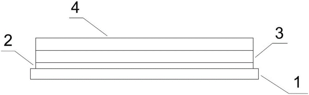
图1为带有电铸层的基板结构示意图;Fig. 1 is a schematic diagram of the structure of a substrate with an electroforming layer;
其中:in:
1.载体,2.光敏胶,3.母版,4.工作版。1. Carrier, 2. Photosensitive adhesive, 3. Master, 4. Working.
具体实施方式Detailed ways
下面结合附图和实施例,对本发明的具体实施方式作进一步详细描述。以下实施例用于说明本发明,但不用来限制本发明的范围。The specific embodiments of the present invention will be described in further detail below with reference to the accompanying drawings and embodiments. The following examples are intended to illustrate the present invention, but not to limit the scope of the present invention.
本发明实施例公开了一种工作版的防皱电铸工艺,包括如下步骤:The embodiment of the present invention discloses an anti-wrinkle electroforming process for a working plate, comprising the following steps:
A、将待电铸的母版3通过光敏胶2平整地粘附于至少部分透光的载体1上,得到基板;A. The master plate 3 to be electroformed is evenly adhered to the at least partially transparent carrier 1 through the photosensitive adhesive 2 to obtain a substrate;
B、然后将所述基板进行固化,并且在所述母版3周围贴附导电胶带,得到固化后的基板;B, then the substrate is cured, and a conductive tape is attached around the master 3 to obtain a cured substrate;
C、将所述固化后的基板进行电铸处理,得到电铸层,所得电铸层即为工作版4。C. The solidified substrate is electroformed to obtain an electroformed layer, and the obtained electroformed layer is the working plate 4 .
通过将待电铸的母版3通过光敏胶2平整地粘附于至少部分透光的载体1上,使得底面平整;然后将光敏胶2光固化,可使母版3稳固的固定于载体1上,使待电铸的母版3版面保持高的平整度。By flatly adhering the master 3 to be electroformed on the at least partially light-transmitting carrier 1 through the photosensitive adhesive 2, the bottom surface is made flat; and then the photosensitive adhesive 2 is light-cured, so that the master 3 can be stably fixed on the carrier 1 , so that the layout of the master 3 to be electroformed maintains a high flatness.
在上述实施例中,所述载体1为透明载体1,利于光敏胶2进行光固化,从而使母版3稳固的固定于载体1上,也进一步确保了母版3的版面保持平整。In the above embodiment, the carrier 1 is a transparent carrier 1, which facilitates the photocuring of the photosensitive adhesive 2, so that the master 3 is stably fixed on the carrier 1, and further ensures that the layout of the master 3 remains flat.
在上述实施例中,所述载体1为PC透明载体1,其具有高的透明度,更有利于光敏胶2进行光固化,从而使母版3更加稳固的固定于载体1上,也更进一步确保了母版3的版面保持平整。In the above embodiment, the carrier 1 is a PC transparent carrier 1, which has high transparency, which is more conducive to the photocuring of the photosensitive adhesive 2, so that the master plate 3 is more firmly fixed on the carrier 1, and further ensures that the The layout of Master 3 remains flat.
在上述实施例中,电铸处理的电流为60‐140A。In the above-mentioned embodiment, the electric current of the electroforming process is 60-140A.
在上述实施例中,电铸处理的时间为2‐24h。In the above embodiment, the electroforming treatment time is 2-24h.
在上述实施例中,电铸层的厚度为50‐500μm。In the above embodiments, the thickness of the electroformed layer is 50-500 μm.
在上述实施例中,所述步骤C中,将所述固化后的基板进行电铸处理后,得到带有电铸层的基板,将所述电铸层与所述基板上的母版分离,所得电铸层即为工作版4。In the above embodiment, in the step C, after the solidified substrate is subjected to electroforming treatment, a substrate with an electroforming layer is obtained, and the electroforming layer is separated from the master on the substrate, The resulting electroformed layer is the working version 4.
在上述实施例中,所述步骤A中,将所述载体1上母版3周边的光敏胶2除去。In the above embodiment, in the step A, the photosensitive adhesive 2 around the master 3 on the carrier 1 is removed.
在上述实施例中,所述待电铸的母版3为镍母版3,所述电铸层为镍电铸层。In the above embodiment, the master 3 to be electroformed is a nickel master 3, and the electroforming layer is a nickel electroforming layer.
为了更好的说明本发明的技术方案,下面将几个具体的实施例方式。In order to better illustrate the technical solutions of the present invention, several specific embodiments are described below.
具体实施例一Specific embodiment one
在1000mm*800mm的透明PC板载体1上涂布UV胶,将待电铸的镍母版3通过UV胶平整地粘附在PC板载体1上,擦除镍母版3以外的UV胶,得到基板,然后将PC板载体1反置,通过紫外线光透过PC板载体1将UV胶进行光固化,得到固化后的基板,可使镍母版3稳固的固定于PC板载体1上,使镍母版3版面保持高的平整度。然后在镍母版3的四周粘贴导电胶带,将固化后的基板置于电铸槽中进行电铸处理。Apply UV glue on the transparent PC board carrier 1 of 1000mm*800mm, and flatly adhere the nickel master 3 to be electroformed on the PC board carrier 1 through the UV glue, erase the UV glue other than the nickel master 3, The substrate is obtained, and then the PC board carrier 1 is inverted, and the UV glue is photocured through the PC board carrier 1 by ultraviolet light to obtain a cured substrate, so that the nickel master 3 can be stably fixed on the PC board carrier 1, Keep the nickel master 3 layout high flatness. Then, a conductive tape is pasted around the nickel master 3, and the cured substrate is placed in an electroforming tank for electroforming treatment.
电铸槽中的电铸液为氨基磺酸镍,调节电流为110A,电压为7V,当电铸处理时间达到4h,完成电铸处理,得到带有电铸层的基板。The electroforming solution in the electroforming tank is nickel sulfamate, the regulating current is 110A, and the voltage is 7V. When the electroforming treatment time reaches 4h, the electroforming treatment is completed, and a substrate with an electroforming layer is obtained.
将带有电铸层的基板取出,剥离电铸层,将电铸层与基板上的镍母版3分离,即可得到120μm厚、与镍母版3具有互补全息图案的镍工作版4。The substrate with the electroforming layer was taken out, the electroforming layer was peeled off, and the electroforming layer was separated from the nickel master 3 on the substrate to obtain a nickel working plate 4 with a thickness of 120 μm and a complementary holographic pattern with the nickel master 3 .
具体实施例二Specific embodiment two
可同样参考第一实施例方式,本第二实施例方式的工作版的防皱电铸工艺与第一实施例方式的区别仅在于:电铸处理中,调节电流为60A,电压为8V,当电铸处理时间达到2h,完成电铸处理,得到带有电铸层的基板。将带有电铸层的基板取出,剥离电铸层,将电铸层与基板上的镍母版3分离,即可得到50μm厚、与镍母版3具有互补全息图案的镍工作版4。Reference can also be made to the first embodiment. The difference between the wrinkle-proof electroforming process of the working plate of the second embodiment and the first embodiment is that in the electroforming process, the regulated current is 60A and the voltage is 8V. The electroforming treatment time reaches 2h, the electroforming treatment is completed, and a substrate with an electroforming layer is obtained. Take out the substrate with the electroformed layer, peel off the electroformed layer, and separate the electroformed layer from the nickel master 3 on the substrate to obtain a nickel working plate 4 with a thickness of 50 μm and a complementary holographic pattern with the nickel master 3 .
具体实施例三Specific embodiment three
可同样参考第一实施例方式,本第三实施例方式的工作版的防皱电铸工艺与第一实施例方式的区别仅在于:电铸处理中,调节电流为140A,电压为7V,当电铸处理时间达到24h,完成电铸处理,得到带有电铸层的基板。将带有电铸层的基板取出,剥离电铸层,将电铸层与基板上的镍母版3分离,即可得到500μm厚、与镍母版3具有互补全息图案的镍工作版4。The first embodiment can also be referred to. The difference between the wrinkle-proof electroforming process of the working plate of the third embodiment and the first embodiment is only that in the electroforming process, the regulated current is 140A and the voltage is 7V. The electroforming treatment time reaches 24h, the electroforming treatment is completed, and a substrate with an electroforming layer is obtained. Take out the substrate with the electroformed layer, peel off the electroformed layer, and separate the electroformed layer from the nickel master 3 on the substrate to obtain a nickel working plate 4 with a thickness of 500 μm and a complementary holographic pattern with the nickel master 3 .
具体实施例四Specific embodiment four
采用日立电子公司的JSM‐6460LV型扫描电镜,观测实施例一至实施例三中不同批次所得镍工作版4以及对比例一不同批次的工作版的表面形貌,并采用Image Tool软件测量其平均晶粒尺寸,其中对比例一为,母版采用双面胶固定在载体上电铸法制作工作版,结果如下述表1所示。The JSM-6460LV scanning electron microscope from Hitachi Electronics was used to observe the surface topography of the nickel working plates 4 obtained in different batches in Example 1 to Example 3 and the working plates of different batches in Comparative Example 1, and the Image Tool software was used to measure the surface topography. The average grain size, in Comparative Example 1, the master plate was fixed on the carrier with double-sided tape to make a working plate by electroforming, and the results are shown in Table 1 below.
表1Table 1
从上述表1可以看出,相比对比例一所得工作版,实施例一至实施例三所得工作版均平均晶粒尺寸较小,表面形貌较为平整,工作版平整度较高,尤其实施例一工作版平整度最高。As can be seen from the above Table 1, compared with the working plates obtained in Comparative Example 1, the average grain size of the working plates obtained in Examples 1 to 3 is smaller, the surface morphology is relatively flat, and the flatness of the working plates is higher, especially the Examples A working version has the highest flatness.
以上所述实施例的各技术特征可以进行任意的组合,为使描述简洁,未对上述实施例中的各个技术特征所有可能的组合都进行描述,然而,只要这些技术特征的组合不存在矛盾,都应当认为是本说明书记载的范围。The technical features of the above-described embodiments can be combined arbitrarily. For the sake of brevity, all possible combinations of the technical features in the above-described embodiments are not described. However, as long as there is no contradiction between the combinations of these technical features, All should be regarded as the scope described in this specification.
以上所述实施例仅表达了本发明的几种实施方式,其描述较为具体和详细,但并不能因此而理解为对发明专利范围的限制。应当指出的是,对于本领域的普通技术人员来说,在不脱离本发明构思的前提下,还可以做出若干变形和改进,这些都属于本发明的保护范围。因此,本发明专利的保护范围应以所附权利要求为准。The above-mentioned embodiments only represent several embodiments of the present invention, and the descriptions thereof are more specific and detailed, but should not be construed as a limitation on the scope of the invention patent. It should be pointed out that for those skilled in the art, without departing from the concept of the present invention, several modifications and improvements can be made, which all belong to the protection scope of the present invention. Therefore, the protection scope of the patent of the present invention should be subject to the appended claims.
Claims (9)
Priority Applications (1)
| Application Number | Priority Date | Filing Date | Title |
|---|---|---|---|
| CN201810832953.2A CN110760896A (en) | 2018-07-26 | 2018-07-26 | Crease-resistant electroforming process for working plate |
Applications Claiming Priority (1)
| Application Number | Priority Date | Filing Date | Title |
|---|---|---|---|
| CN201810832953.2A CN110760896A (en) | 2018-07-26 | 2018-07-26 | Crease-resistant electroforming process for working plate |
Publications (1)
| Publication Number | Publication Date |
|---|---|
| CN110760896A true CN110760896A (en) | 2020-02-07 |
Family
ID=69327462
Family Applications (1)
| Application Number | Title | Priority Date | Filing Date |
|---|---|---|---|
| CN201810832953.2A Pending CN110760896A (en) | 2018-07-26 | 2018-07-26 | Crease-resistant electroforming process for working plate |
Country Status (1)
| Country | Link |
|---|---|
| CN (1) | CN110760896A (en) |
Cited By (1)
| Publication number | Priority date | Publication date | Assignee | Title |
|---|---|---|---|---|
| CN112080767A (en) * | 2020-11-16 | 2020-12-15 | 湖南和锐镭射科技有限公司 | Manufacturing method of high-brightness chromatic-aberration-free laser film |
Citations (45)
| Publication number | Priority date | Publication date | Assignee | Title |
|---|---|---|---|---|
| JPH08334903A (en) * | 1995-06-05 | 1996-12-17 | Think Lab Kk | Screen plate and its production |
| CN1456711A (en) * | 2002-04-11 | 2003-11-19 | 希普利公司 | Electroplating method |
| CN1512920A (en) * | 2001-05-31 | 2004-07-14 | 3M | Dimensionally stable composite article and method of making same |
| JP2004225106A (en) * | 2003-01-23 | 2004-08-12 | Japan Steel Works Ltd:The | Manufacturing method of stamper |
| CN1530947A (en) * | 2003-03-14 | 2004-09-22 | 光群雷射科技股份有限公司 | Impression mother set with grain pattern and its making method and plate assembling method |
| CN101016634A (en) * | 2006-12-30 | 2007-08-15 | 苏州大学 | Method of preparing metal roller with surface relief microstructure |
| CN101126820A (en) * | 2007-09-07 | 2008-02-20 | 中国科学院长春光学精密机械与物理研究所 | A kind of process method of making aspheric mirror by adopting replication technology |
| CN101304867A (en) * | 2005-09-20 | 2008-11-12 | 富士胶片株式会社 | Method for manufacturing embossed sheet and apparatus thereof, method for manufacturing patterned sheet, and patterned sheet |
| CN101450841A (en) * | 2007-11-29 | 2009-06-10 | 比亚迪股份有限公司 | Method for coating ultraviolet light curing glue on substrate and method for attaching film |
| CN101474933A (en) * | 2009-01-01 | 2009-07-08 | 黄汉祥 | Production method of ecological simulation diamond plate |
| CN101517130A (en) * | 2006-08-07 | 2009-08-26 | 精工电子有限公司 | Method for manufacturing electroformed mold, electroformed mold, and method for manufacturing electroformed parts |
| CN101618628A (en) * | 2009-08-11 | 2010-01-06 | 湖北兴龙包装材料有限责任公司 | Method for manufacturing holographic mother board by using electroforming imposition |
| CN201410774Y (en) * | 2009-04-29 | 2010-02-24 | 汕头市壮丽印刷有限公司 | Cathode carrier plate on electroforming plane of conductive upper interlayer-type laser nickel plate |
| CN101900935A (en) * | 2009-05-27 | 2010-12-01 | 比亚迪股份有限公司 | Ultraviolet impressing method and device thereof |
| CN101929833A (en) * | 2009-06-25 | 2010-12-29 | 淮阴工学院 | Eddy Current Sensors for Metal Gap and Defect Detection at High Temperatures and Narrow Gap Conditions |
| CN101983866A (en) * | 2010-08-16 | 2011-03-09 | 郑健生 | Film compounding process |
| CN101992583A (en) * | 2009-08-19 | 2011-03-30 | 比亚迪股份有限公司 | Method for preparing seamless wide-width holographic embossing master plate |
| CN102009517A (en) * | 2010-09-20 | 2011-04-13 | 苏州苏大维格光电科技股份有限公司 | Method for making metal mother board |
| CN102208540A (en) * | 2011-04-18 | 2011-10-05 | 电子科技大学 | Substrate for flexible photoelectronic device and preparation method thereof |
| CN102208563A (en) * | 2011-04-18 | 2011-10-05 | 电子科技大学 | Substrate for flexible luminescent device and preparation method thereof |
| CN202351850U (en) * | 2011-07-25 | 2012-07-25 | 南京华睿川电子科技有限公司 | Light color panel structure of touch screen |
| CN102732916A (en) * | 2011-04-13 | 2012-10-17 | 山东泰宝包装制品有限公司 | Rapid electroforming process |
| CN103147099A (en) * | 2013-03-20 | 2013-06-12 | 南京航空航天大学 | Micro electroforming device and method for positive flushing liquid |
| CN103226288A (en) * | 2013-04-27 | 2013-07-31 | 苏州大学 | UV-curing micro-nano-structure template-splicing device and template-splicing process |
| CN103280522A (en) * | 2013-04-19 | 2013-09-04 | 西安交通大学 | Packaging process capable of improving stability of ionic polymer metal composite (IPMC) driver |
| CN103317825A (en) * | 2013-05-14 | 2013-09-25 | 武汉华工图像技术开发有限公司 | UV makeup method of holographic dedicated plate |
| CN103336418A (en) * | 2013-05-31 | 2013-10-02 | 湖北兴龙包装材料有限责任公司 | UV makeup method and device |
| CN103507393A (en) * | 2013-09-26 | 2014-01-15 | 上海宏盾防伪材料有限公司 | Holographic BOPP mold pressing seamless plate roller and manufacturing method thereof |
| CN103707670A (en) * | 2013-01-31 | 2014-04-09 | 汕头市依明机械股份有限公司 | Laser pattern positioning impression transfer method |
| CN103818873A (en) * | 2014-01-09 | 2014-05-28 | 合肥工业大学 | Processing method of all metal channel microstructure with great thickness and high depth-to-width ratio |
| CN104149481A (en) * | 2014-07-22 | 2014-11-19 | 天津沃特激光防伪标识有限公司 | Laser holography anti-fake film nickel plate slicing method |
| CN104309267A (en) * | 2014-09-17 | 2015-01-28 | 合肥鑫晟光电科技有限公司 | Substrate applying method, touch control display substrate and display apparatus |
| CN104345962A (en) * | 2014-02-24 | 2015-02-11 | 东莞市骏达触控科技有限公司 | Portable electronic product, touch screen and touch screen manufacturing method |
| CN204162817U (en) * | 2014-11-03 | 2015-02-18 | 昆明市荣顺物宇科技有限公司 | A kind of negative plate of improved type electric casting device |
| CN104777707A (en) * | 2015-03-12 | 2015-07-15 | 宁波Gqy视讯股份有限公司 | Bonding method for DLP (digital light processing) combined spliced glass screen |
| CN104807485A (en) * | 2014-01-23 | 2015-07-29 | 丛森 | Novel resin code disc production process |
| CN104816534A (en) * | 2015-03-27 | 2015-08-05 | 信利光电股份有限公司 | Small touch screen making method, and small glass and substrate aligning method |
| CN105405752A (en) * | 2015-12-15 | 2016-03-16 | 苏州大学 | A kind of manufacturing method of flexible nano wire grid type transparent conductive electrode |
| CN106952567A (en) * | 2017-03-29 | 2017-07-14 | 江苏兴广包装科技有限公司 | A kind of holographic positioning composite membrane production method |
| CN106980228A (en) * | 2017-04-25 | 2017-07-25 | 鲁东大学 | A kind of method that durability micro-nano structure is prepared on bend glass |
| CN107219692A (en) * | 2017-07-28 | 2017-09-29 | 京东方科技集团股份有限公司 | A kind of liquid crystal panel and liquid crystal display device |
| CN107362812A (en) * | 2017-07-25 | 2017-11-21 | 苏州大学 | A kind of compound two-dimensional material of selenium sulfuration rhenium, preparation method and applications |
| CN107429418A (en) * | 2014-11-12 | 2017-12-01 | 安托士设备系统公司 | Simultaneous hydrophilic modification of photoresist surfaces and metal surface preparation: methods, systems and products |
| CN109983407A (en) * | 2016-11-30 | 2019-07-05 | 株式会社Lg化学 | Hologram duplicating method and hologram duplicating apparatus |
| CN110871619A (en) * | 2018-08-29 | 2020-03-10 | 苏州苏大维格科技集团股份有限公司 | High-fidelity makeup method |
-
2018
- 2018-07-26 CN CN201810832953.2A patent/CN110760896A/en active Pending
Patent Citations (45)
| Publication number | Priority date | Publication date | Assignee | Title |
|---|---|---|---|---|
| JPH08334903A (en) * | 1995-06-05 | 1996-12-17 | Think Lab Kk | Screen plate and its production |
| CN1512920A (en) * | 2001-05-31 | 2004-07-14 | 3M | Dimensionally stable composite article and method of making same |
| CN1456711A (en) * | 2002-04-11 | 2003-11-19 | 希普利公司 | Electroplating method |
| JP2004225106A (en) * | 2003-01-23 | 2004-08-12 | Japan Steel Works Ltd:The | Manufacturing method of stamper |
| CN1530947A (en) * | 2003-03-14 | 2004-09-22 | 光群雷射科技股份有限公司 | Impression mother set with grain pattern and its making method and plate assembling method |
| CN101304867A (en) * | 2005-09-20 | 2008-11-12 | 富士胶片株式会社 | Method for manufacturing embossed sheet and apparatus thereof, method for manufacturing patterned sheet, and patterned sheet |
| CN101517130A (en) * | 2006-08-07 | 2009-08-26 | 精工电子有限公司 | Method for manufacturing electroformed mold, electroformed mold, and method for manufacturing electroformed parts |
| CN101016634A (en) * | 2006-12-30 | 2007-08-15 | 苏州大学 | Method of preparing metal roller with surface relief microstructure |
| CN101126820A (en) * | 2007-09-07 | 2008-02-20 | 中国科学院长春光学精密机械与物理研究所 | A kind of process method of making aspheric mirror by adopting replication technology |
| CN101450841A (en) * | 2007-11-29 | 2009-06-10 | 比亚迪股份有限公司 | Method for coating ultraviolet light curing glue on substrate and method for attaching film |
| CN101474933A (en) * | 2009-01-01 | 2009-07-08 | 黄汉祥 | Production method of ecological simulation diamond plate |
| CN201410774Y (en) * | 2009-04-29 | 2010-02-24 | 汕头市壮丽印刷有限公司 | Cathode carrier plate on electroforming plane of conductive upper interlayer-type laser nickel plate |
| CN101900935A (en) * | 2009-05-27 | 2010-12-01 | 比亚迪股份有限公司 | Ultraviolet impressing method and device thereof |
| CN101929833A (en) * | 2009-06-25 | 2010-12-29 | 淮阴工学院 | Eddy Current Sensors for Metal Gap and Defect Detection at High Temperatures and Narrow Gap Conditions |
| CN101618628A (en) * | 2009-08-11 | 2010-01-06 | 湖北兴龙包装材料有限责任公司 | Method for manufacturing holographic mother board by using electroforming imposition |
| CN101992583A (en) * | 2009-08-19 | 2011-03-30 | 比亚迪股份有限公司 | Method for preparing seamless wide-width holographic embossing master plate |
| CN101983866A (en) * | 2010-08-16 | 2011-03-09 | 郑健生 | Film compounding process |
| CN102009517A (en) * | 2010-09-20 | 2011-04-13 | 苏州苏大维格光电科技股份有限公司 | Method for making metal mother board |
| CN102732916A (en) * | 2011-04-13 | 2012-10-17 | 山东泰宝包装制品有限公司 | Rapid electroforming process |
| CN102208540A (en) * | 2011-04-18 | 2011-10-05 | 电子科技大学 | Substrate for flexible photoelectronic device and preparation method thereof |
| CN102208563A (en) * | 2011-04-18 | 2011-10-05 | 电子科技大学 | Substrate for flexible luminescent device and preparation method thereof |
| CN202351850U (en) * | 2011-07-25 | 2012-07-25 | 南京华睿川电子科技有限公司 | Light color panel structure of touch screen |
| CN103707670A (en) * | 2013-01-31 | 2014-04-09 | 汕头市依明机械股份有限公司 | Laser pattern positioning impression transfer method |
| CN103147099A (en) * | 2013-03-20 | 2013-06-12 | 南京航空航天大学 | Micro electroforming device and method for positive flushing liquid |
| CN103280522A (en) * | 2013-04-19 | 2013-09-04 | 西安交通大学 | Packaging process capable of improving stability of ionic polymer metal composite (IPMC) driver |
| CN103226288A (en) * | 2013-04-27 | 2013-07-31 | 苏州大学 | UV-curing micro-nano-structure template-splicing device and template-splicing process |
| CN103317825A (en) * | 2013-05-14 | 2013-09-25 | 武汉华工图像技术开发有限公司 | UV makeup method of holographic dedicated plate |
| CN103336418A (en) * | 2013-05-31 | 2013-10-02 | 湖北兴龙包装材料有限责任公司 | UV makeup method and device |
| CN103507393A (en) * | 2013-09-26 | 2014-01-15 | 上海宏盾防伪材料有限公司 | Holographic BOPP mold pressing seamless plate roller and manufacturing method thereof |
| CN103818873A (en) * | 2014-01-09 | 2014-05-28 | 合肥工业大学 | Processing method of all metal channel microstructure with great thickness and high depth-to-width ratio |
| CN104807485A (en) * | 2014-01-23 | 2015-07-29 | 丛森 | Novel resin code disc production process |
| CN104345962A (en) * | 2014-02-24 | 2015-02-11 | 东莞市骏达触控科技有限公司 | Portable electronic product, touch screen and touch screen manufacturing method |
| CN104149481A (en) * | 2014-07-22 | 2014-11-19 | 天津沃特激光防伪标识有限公司 | Laser holography anti-fake film nickel plate slicing method |
| CN104309267A (en) * | 2014-09-17 | 2015-01-28 | 合肥鑫晟光电科技有限公司 | Substrate applying method, touch control display substrate and display apparatus |
| CN204162817U (en) * | 2014-11-03 | 2015-02-18 | 昆明市荣顺物宇科技有限公司 | A kind of negative plate of improved type electric casting device |
| CN107429418A (en) * | 2014-11-12 | 2017-12-01 | 安托士设备系统公司 | Simultaneous hydrophilic modification of photoresist surfaces and metal surface preparation: methods, systems and products |
| CN104777707A (en) * | 2015-03-12 | 2015-07-15 | 宁波Gqy视讯股份有限公司 | Bonding method for DLP (digital light processing) combined spliced glass screen |
| CN104816534A (en) * | 2015-03-27 | 2015-08-05 | 信利光电股份有限公司 | Small touch screen making method, and small glass and substrate aligning method |
| CN105405752A (en) * | 2015-12-15 | 2016-03-16 | 苏州大学 | A kind of manufacturing method of flexible nano wire grid type transparent conductive electrode |
| CN109983407A (en) * | 2016-11-30 | 2019-07-05 | 株式会社Lg化学 | Hologram duplicating method and hologram duplicating apparatus |
| CN106952567A (en) * | 2017-03-29 | 2017-07-14 | 江苏兴广包装科技有限公司 | A kind of holographic positioning composite membrane production method |
| CN106980228A (en) * | 2017-04-25 | 2017-07-25 | 鲁东大学 | A kind of method that durability micro-nano structure is prepared on bend glass |
| CN107362812A (en) * | 2017-07-25 | 2017-11-21 | 苏州大学 | A kind of compound two-dimensional material of selenium sulfuration rhenium, preparation method and applications |
| CN107219692A (en) * | 2017-07-28 | 2017-09-29 | 京东方科技集团股份有限公司 | A kind of liquid crystal panel and liquid crystal display device |
| CN110871619A (en) * | 2018-08-29 | 2020-03-10 | 苏州苏大维格科技集团股份有限公司 | High-fidelity makeup method |
Non-Patent Citations (3)
| Title |
|---|
| WANG, H.A,B 等: ""Temperature sensing property of hollow-core photonic bandgap fiber filled with CdSe/ZnS quantum dots in an UV curing adhesive"", 《OPTICAL FIBER TECHNOLOGY》 * |
| 剧永波 等: ""LTPS工艺中光刻胶与膜层粘附力的研究"", 《液晶与显示》 * |
| 王跃川 等: ""光固化粘合剂——机遇与挑战"", 《粘接》 * |
Cited By (1)
| Publication number | Priority date | Publication date | Assignee | Title |
|---|---|---|---|---|
| CN112080767A (en) * | 2020-11-16 | 2020-12-15 | 湖南和锐镭射科技有限公司 | Manufacturing method of high-brightness chromatic-aberration-free laser film |
Similar Documents
| Publication | Publication Date | Title |
|---|---|---|
| JP6010580B2 (en) | LIGA-UV manufacturing method of multilayer metal structure in which adjacent layers do not completely overlap and structure obtained thereby | |
| CN102459713B (en) | Method for manufacturing a metal microstructure and microstructure obtained according to said method | |
| TWI826477B (en) | Methods of making metal patterns on flexible substrate | |
| CN102147569B (en) | Processing method of micro-component in multi-layer structure and solidified SU-8 photoresist sheet | |
| JP2015222836A (en) | Imprint method and imprint mold manufacturing method | |
| CN110802912A (en) | Laser plate making method | |
| CN101456329B (en) | Method of fabricating mask for forming wood grain patterns | |
| CN110760896A (en) | Crease-resistant electroforming process for working plate | |
| JP2008230083A (en) | Stamper manufacturing method | |
| CN101918222A (en) | Process for preparing gravure printing plates for offset printing | |
| EP3330794A1 (en) | Photomask, laminate comprising photomask, photomask preparation method, pattern forming apparatus using photomask and pattern forming method using photomask | |
| US2765230A (en) | Method of forming matrices for the electrodeposition of grids | |
| CN114561672B (en) | Electrochemical additive manufacturing method and device for preparing confinement patterns based on photolithographic layering | |
| TWI614118B (en) | Method for inspecting substrate for mold for die imprinting and substrate for mold | |
| CN113562686A (en) | Manufacturing method of 3D-MEMS probe | |
| JPH1034870A (en) | Manufacturing method of electroformed products | |
| TWI233423B (en) | Method of fabricating a stamper with microstructure patterns | |
| JP3124618B2 (en) | Method and apparatus for producing sheet-shaped duplication mold by electroforming | |
| JP3364195B2 (en) | Patterned electrodeposited image and manufacturing method thereof | |
| KR20110115864A (en) | Manufacturing method of micro parts and mold | |
| US20210047745A1 (en) | Electrochemical additive manufacturing of articles | |
| JP3061207B2 (en) | Manufacturing method of electroformed products | |
| JPH07331479A (en) | Formation of electrodeposited image | |
| Tang et al. | Fabrication of membrane-typed metal mould with microstructures and application for roller imprinting | |
| CN106350769B (en) | A kind of metal shadow mask and preparation method thereof |
Legal Events
| Date | Code | Title | Description |
|---|---|---|---|
| PB01 | Publication | ||
| PB01 | Publication | ||
| SE01 | Entry into force of request for substantive examination | ||
| SE01 | Entry into force of request for substantive examination | ||
| RJ01 | Rejection of invention patent application after publication |
Application publication date: 20200207 |
|
| RJ01 | Rejection of invention patent application after publication |